TL H 11057
LM615
Quad
Comparator
and
Adjustable
Reference
December 1994
LM615 Quad Comparator and Adjustable Reference
General Description
The comparators have an input range which extends to the
negative supply and have open-collector outputs Improved
over the LM139 series the input stages of the comparators
have lateral PNP input transistors which enable low input
currents for large differential input voltages and swings
above V
a
The voltage reference is a three-terminal shunt-type band-
gap and is referred to the V
b
terminal Two resistors pro-
gram the reference from 1 24V to 6 3V with accuracy of
g
0 6% available The reference features operation over a
shunt current range of 17 mA to 20 mA low dynamic imped-
ance broad capacitive load range and cathode terminal
voltage ranging from a diode-drop below V
b
to above V
a
As a member of National's Super-Block
TM
family
the
LM615 is a space-saving monolithic alternative to a multi-
chip solution offering a high level of integration without sac-
rificing performance
Features
COMPARATORS
Y
Low operating current
600 mA
Y
Wide supply voltage range
4V to 36V
Y
Open-collector outputs
Y
Input common-mode range
V
b
to (V
a
b
1 8V)
Y
Wide differential input voltage
g
36V
REFERENCE
Y
Adjustable output voltage
1 24V to 6 3V
Y
Tight initial tolerance available
g
0 6% (25 C)
Y
Wide operating current range
17 mA to 20 mA
Y
Tolerant of load capacitance
Applications
Y
Adjustable threshold detector
Y
Time-delay generator
Y
Voltage window comparator
Y
Power supply monitor
Y
RGB level detector
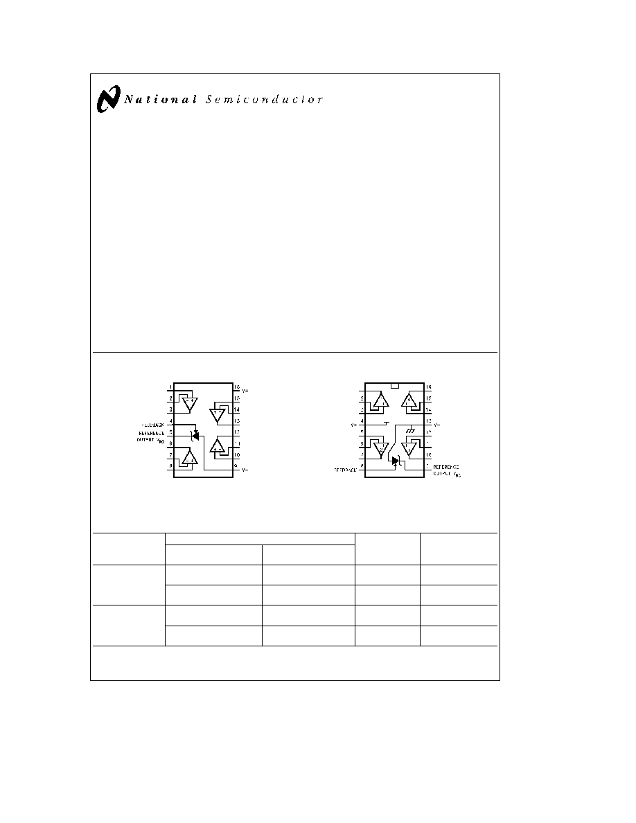
Connection Diagram
M Package
TL H 11057 � 24
Top View
N Package
TL H 11057 � 1
Top View
Ordering Information
For information about surface-mount packaging of this device please contact the
Analog Product Marketing group at National Semiconductor Corp headquarters
Reference
Temperature Range
NSC
Tolerances
Military
Industrial
Package
Package Number
b
55 C
s
T
J
s
a
125 C
b
40 C
s
T
J
s
a
85 C
g
0 6% at 25 C
LM615AMN
LM615AIN
16-Pin
N16A
80 ppm C max
Molded DIP
LM615AMJ 883
16-Pin
J16A
(Note 13)
Ceramic DIP
g
2 0% at 25 C
LM615MN
LM615IN
16-Pin
N16A
150 ppm C max
Molded DIP
LM615IM
16-Pin Narrow
M16A
Surface Mount
Super-Block
TM
is a trademark of National Semiconductor Corporation
C1995 National Semiconductor Corporation
RRD-B30M115 Printed in U S A
Absolute Maximum Ratings
(Note 1)
If Military Aerospace specified devices are required
please contact the National Semiconductor Sales
Office Distributors for availability and specifications
Voltage on Any Pin Except V
RO
(referred to V
b
pin)
(Note 2)
36V (Max)
(Note 3)
b
0 3V (Min)
Current through Any Input Pin
and V
RO
Pin
g
20 mA
Differential Input Voltage
g
36V
Output Short-Circuit Duration
(Note 4)
Storage Temperature Range
b
65 C
s
T
J
s
a
150 C
Maximum Junction Temperature
150 C
Thermal Resistance Junction-to-Ambient (Note 5)
N Package
95 C W
Soldering Information
N Package Soldering (10 seconds)
260 C
ESD Tolerance (Note 6)
g
1 kV
Operating Temperature Range
LM615AI LM615I
b
40 C
s
T
J
s
a
85 C
LM615A LM615M
b
55 C
s
T
J
s
a
125 C
Electrical Characteristics
These specifications apply for V
b
e
GND
e
0V V
a
e
5V V
CM
e
V
OUT
e
V
a
2 I
R
e
100 mA FEEDBACK pin shorted to
GND unless otherwise specified Limits in standard typeface are for T
J
e
25 C limits in boldface type apply over the
Operating Temperature Range
LM615AM
LM615M
Symbol
Parameter
Conditions
Typical
LM615AI
LM615I
Units
(Note 7)
Limits
Limits
(Note 8)
(Note 8)
COMPARATORS
I
S
Total Supply Current
V
a
Current R
LOAD
e
%
250
550
600
m
A max
3V
s
V
a
s
36V
350
600
650
m
A max
V
OS
Offset Voltage over
4V
s
V
a s
36V R
L
e
15 kX
1 0
3 0
5 0
mV max
V
a
Range
2 0
6 0
7 0
mV max
V
OS
Offset Voltage over
0V
s
V
CM
s
(V
a
b
1 8V)
1 0
3 0
5 0
mV max
V
CM
Range
V
a
e
30V R
L
e
15 kX
1 5
6 0
7 0
mV max
D
V
OS
D
T
Average Offset
15
m
V C
Voltage Drift
I
B
Input Bias Current
b
5
25
35
nA max
b
8
30
40
nA max
I
OS
Input Offset Current
0 2
4
4
nA max
0 3
5
5
nA max
A
V
Voltage Gain
R
L
e
10 kX to 36V
500
50
50
V mV
2V
s
V
OUT
s
27V
min
100
V mV
t
R
Large Signal
V
a
IN
e
1 4V V
b
IN
e
TTL
1 5
m
s
Response Time
Swing R
L
e
5 1 kX
2 0
m
s
I
SINK
Output Sink Current
V
a
IN
e
0V V
b
IN
e
1V
20
10
10
mA min
V
OUT
e
1 5V
13
8
8
mA min
V
OUT
e
0 4V
2 8
1 0
0 8
mA min
2 4
0 5
0 5
mA min
I
L
Output Leakage
V
a
IN
e
1V V
b
IN
e
0V
0 1
10
10
m
A max
Current
V
OUT
e
36V
0 2
m
A
2
Electrical Characteristics
These specifications apply for V
b
e
GND
e
0V V
a
e
5V V
CM
e
V
OUT
e
V
a
2 I
R
e
100 mA FEEDBACK pin shorted to
GND unless otherwise specified Limits in standard typeface are for T
J
e
25 C limits in boldface type apply over the
Operating Temperature Range
(Continued)
LM615AM
LM615M
Symbol
Parameter
Conditions
Typical
LM615AI
LM615I
Units
(Note 7)
Limits
Limits
(Note 8)
(Note 8)
VOLTAGE REFERENCE
(Note 9)
V
R
Reference
1 244
1 2365
1 2191
V min
Voltage
1 2515
1 2689
V max
(
g
0 6%)
(
g
2%)
D
V
R
D
T
Average Drift
(Note 10)
18
80
150
ppm C
with Temperature
max
D
V
R
kH
Average Drift
T
J
e
40 C
400
ppm kH
with Time
T
J
e
150 C
1000
ppm kH
D
V
R
D
T
J
Hysteresis
(Note 11)
3 2
m
V C
D
V
R
D
I
R
V
R
Change
V
R 100 mA
b
V
R 17 mA
0 05
1
1
mV max
with Current
0 1
1 1
1 1
mV max
V
R 10 mA
b
V
R 100 mA
1 5
5
5
mV max
(Note 12)
2 0
5 5
5 5
mV max
R
Resistance
D
V
R 10 mA to 0 1 mA
9 9 mA
0 2
0 56
0 56
X
max
D
V
R 100 mA to 17 mA
83 mA
0 6
13
13
X
max
D
V
R
D
V
RO
V
R
Change
V
R VRO e VR
b
V
R VRO e 6 3V
2 5
5
5
mV max
with V
RO
2 8
10
10
mV max
D
V
R
D
V
a
V
R
Change
V
R Va e 5V
b
V
R Va e 36V
0 1
1 2
1 2
mV max
with V
a
Change
0 1
1 3
1 3
mV max
V
R Va e 5V
b
V
R Va e 3V
0 01
1
1
mV max
0 01
1 5
1 5
mV max
I
FB
FEEDBACK
V
b s
V
FB
s
5 06V
22
35
50
nA max
Bias Current
29
40
55
nA max
e
n
Voltage Noise
BW
e
10 Hz to 10 kHz
30
m
V
RMS
Note 1
Absolute maximum ratings indicate limits beyond which damage to the component may occur Electrical specifications do not apply when operating the
device beyond its rated operating conditions
Note 2
Input voltage above V
a
is allowed As long as one input pin voltage remains inside the common-mode range the comparator will deliver the correct output
Note 3
More accurately it is excessive current flow with resulting excess heating that limits the voltages on all pins When any pin is pulled a diode drop below
V
b
a parasitic NPN transistor turns ON No latch-up will occur as long as the current through that pin remains below the Maximum Rating Operation is undefined
and unpredictable when any parasitic diode or transistor is conducting
Note 4
Shorting an Output to V
b
will not cause power dissipation so it may be continuous However shorting an Output to any more positive voltage (including
V
a
) will cause 80 mA (typ ) to be drawn through the output transistor This current multiplied by the applied voltage is the power dissipation in the output transistor
If the total power from all shorted outputs causes the junction temperature to exceed 150 C degraded reliability or destruction of the device may occur To
determine junction temperature see Note 5
Note 5
Junction temperature may be calculated using T
J
e
T
A
a
P
D
i
JA
The given thermal resistance is worst-case for packages in sockets in still air For
packages soldered to copper-clad board with dissipation from one comparator or reference output transistor nominal i
JA
is 80 C W for the N package
Note 6
Human body model 100 pF discharge through a 1 5 kX resistor
Note 7
Typical values in standard typeface are for T
J
e
25 C values in boldface type apply for the full operating temperature range These values represent the
most likely parametric norm
Note 8
All limits are guaranteed for T
J
e a
25 C (standard type face) or over the full operating temperature range (bold type face)
Note 9
V
RO
is the reference output voltage which may be set for 1 2V to 6 3V (see Application Information) V
R
is the V
RO
-to-FEEDBACK voltage (nominally
1 244V)
Note 10
Average reference drift is calculated from the measurement of the reference voltage at 25 C and at the temperature extremes The drift in ppm C is
10
6
D
V
R
V
R 25 C
D
T
J
where DV
R
is the lowest value subtracted from the highest V
R 25 C
is the value at 25 C and DT
J
is the temperature range This
parameter is guaranteed by design and sample testing
Note 11
Hysteresis is the change in V
RO
caused by a change in T
J
after the reference has been ``dehysterized '' To dehysterize the reference that is minimize the
hysteresis to the typical value its junction temperature should be cycled in the following pattern spiraling in toward 25 C 25 C 85 C
b
40 C 70 C 0 C 25 C
Note 12
Low contact resistance is required for accurate measurement
Note 13
A military RETS electrical test specification is available on request The LM615AMJ 883 may also be procured as a Standard Military Drawing
3
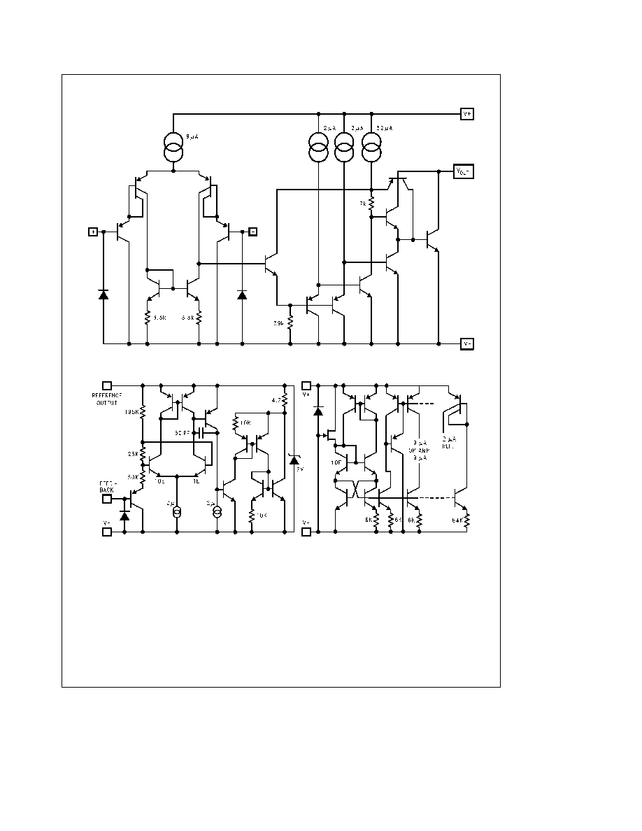
Simplified Schematic Diagrams
Comparator
TL H 11057 � 2
Reference
Bias
TL H 11057 � 3
4
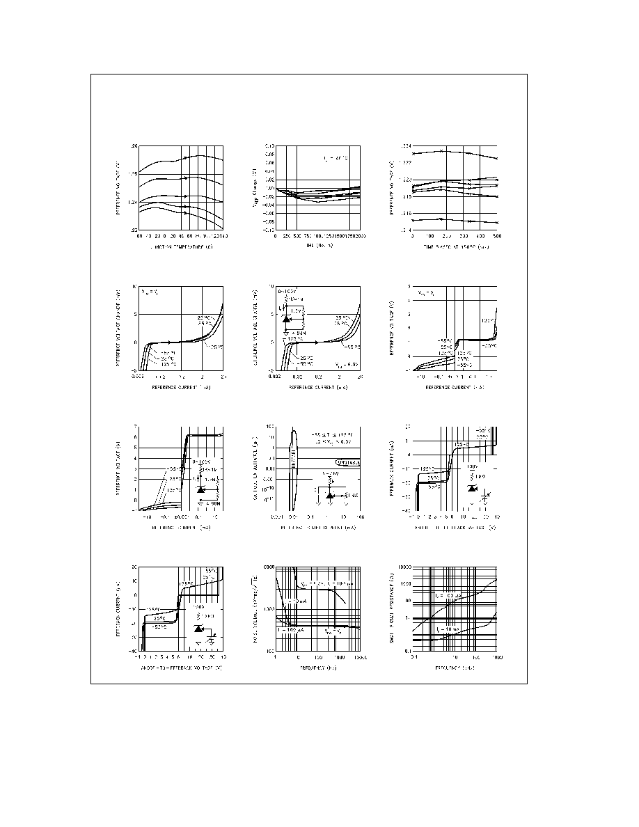
Typical Performance Characteristics (Reference)
T
J
e
25 C FEEDBACK pin shorted to V
b
e
0V unless otherwise noted
vs Temperature
Reference Voltage
Drift vs Time
Reference Voltage
Voltage Drift vs Time
Accelerated Reference
and Temperature
vs Current
Reference Voltage
and Temperature
vs Current
Reference Voltage
vs Reference Current
Reference Voltage
vs Reference Current
Reference Voltage
Stability Range
Reference AC
Voltage
vs FEEDBACK-to-V
b
FEEDBACK Current
Voltage
vs FEEDBACK-to-V
b
FEEDBACK Current
Voltage vs Frequency
Reference Noise
Resistance vs Frequency
Reference Small-Signal
TL H 11057 � 4
5
Typical Performance Characteristics (Reference)
(Continued)
T
J
e
25 C FEEDBACK pin shorted to V
b
e
0V unless otherwise noted
Power-Up Time
Reference
Voltage Step
with FEEDBACK
Reference Voltage
Current Step
with 100 E 12 mA
Reference Voltage
Current Step
for 100 m E 10 mA
Reference Step Response
Voltage Step
Change with Supply
Reference Voltage
TL H 11057 � 5
Typical Performance Characteristics (Comparators)
T
J
e
25 C V
a
e
5V V
b
e
0V unless otherwise noted
vs Supply Voltage
Supply Current
Voltage
Current vs Common-Mode
Input-Bias
Differential Input Voltage
Input Current vs
TL H 11057 � 6
6
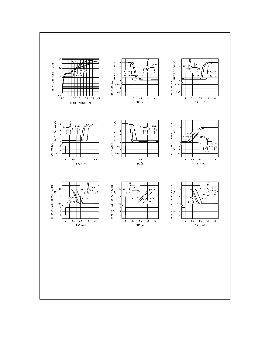
Typical Performance Characteristics (Comparators)
(Continued)
Voltage vs Sink Current
Output Saturation
Negative Transition
Times
Inverting Input
Small-Signal Response
Positive Transition
Times
Inverting Input
Small-Signal Response
Positive Transition
Times Non-Inverting Input
Small-Signal Response
Negative Transition
Times
Non-Inverting Input
Small-Signal Response
Positive Transition
Times
Inverting Input
Large-Signal Response
Negative Transition
Times-Inverting Input
Large-Signal Response
Positive Transition
Times
Non-Inverting Input
Large-Signal Response
Negative Transition
Times
Non-Inverting Input
Large-Signal Response
TL H 11057 � 8
7
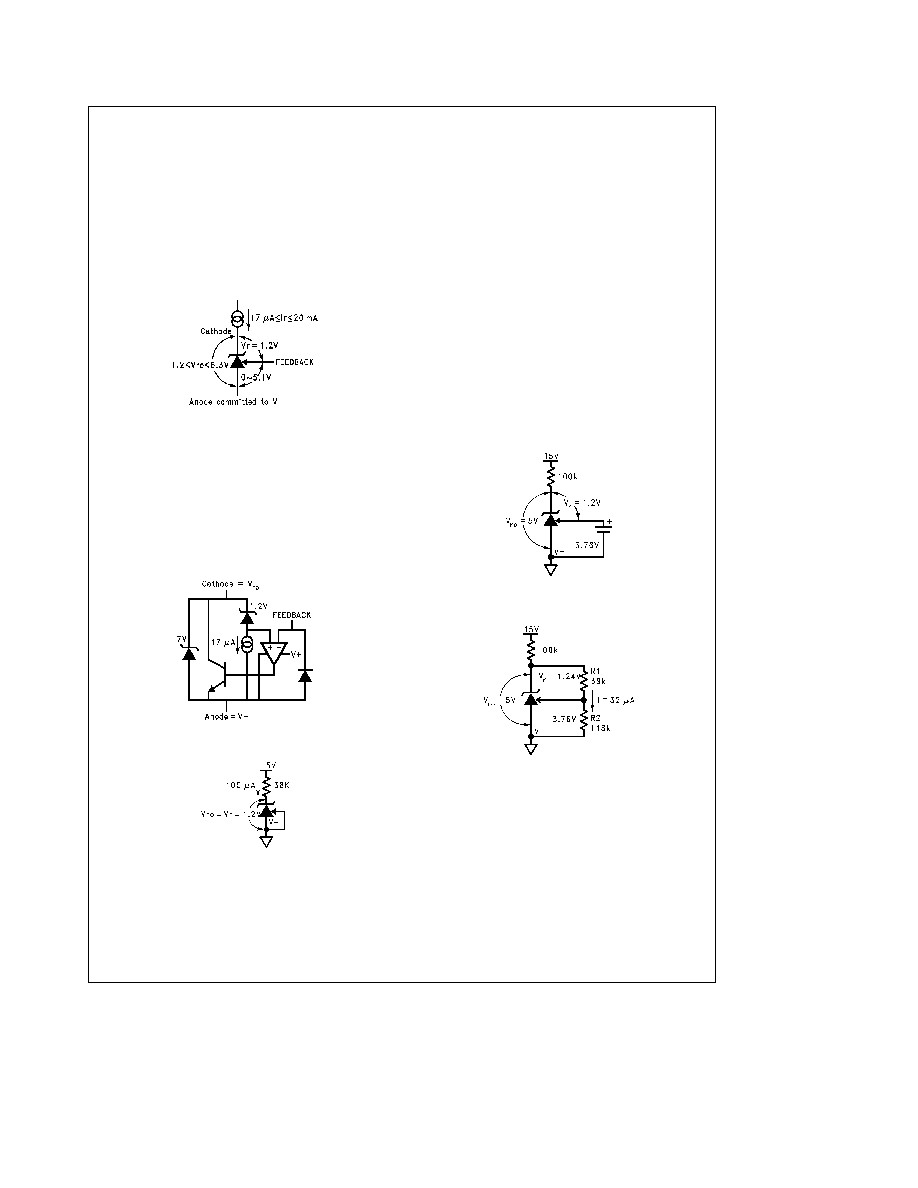
Application Information
VOLTAGE REFERENCE
Reference Biasing
The voltage reference is of a shunt regulator topology that
models as a simple zener diode With current I
r
flowing in
the ``forward'' direction there is the familiar diode transfer
function I
r
flowing in the reverse direction forces the refer-
ence voltage to be developed from cathode to anode The
cathode may swing from a diode drop below V
b
to the ref-
erence voltage or to the avalanche voltage of the parallel
protection diode nominally 7V A 6 3V reference with V
a
e
3V is allowed
TL H 11057 � 9
FIGURE 1 Voltage Associated with Reference
(Current Source I
r
is External)
The reference equivalent circuit reveals how V
r
is held at
the constant 1 2V by feedback and how the FEEDBACK pin
passes little current
To generate the required reverse current typically a resistor
is connected from a supply voltage higher than the refer-
ence voltage Varying that voltage and so varying I
r
has
small effect with the equivalent series resistance of less
than an ohm at the higher currents Alternatively an active
current source such as the LM134 series may generate I
r
TL H 11057 � 10
FIGURE 2 Reference Equivalent Circuit
TL H 11057 � 11
FIGURE 3 1 2V Reference
Capacitors in parallel with the reference are allowed See
the Reference AC Stability Range typical curve for capaci-
tance values
from 20 mA to 3 mA any capacitor value is
stable With the reference's wide stability range with resis-
tive and capacitive loads a wide range of RC filter values
will perform noise filtering
Adjustable Reference
The FEEDBACK pin allows the reference output voltage
V
ro
to vary from 1 24V to 6 3V The reference attempts to
hold V
r
at 1 24V If V
r
is above 1 24V the reference will
conduct current from Cathode to Anode FEEDBACK cur-
rent always remains low If FEEDBACK is connected to An-
ode then V
ro
e
V
r
e
1 24V For higher voltages FEED-
BACK is held at a constant voltage above Anode
say
3 76V for V
ro
e
5V Connecting a resistor across the con-
stant V
r
generates a current I
e
R1 V
r
flowing from Cath-
ode into FEEDBACK node A Thevenin equivalent 3 76V is
generated from FEEDBACK to Anode with R2
e
3 76 I
Keep I greater than one thousand times larger than FEED-
BACK bias current for
k
0 1% error
I
t
32 mA for the mili-
tary grade over the military temperature range (I
t
5 5 mA
for a 1% untrimmed error for an industrial temperature
range part)
TL H 11057 � 12
FIGURE 4 Thevenin Equivalent of
Reference with 5V Output
TL H 11057 � 13
R1
e
V
r
I
e
1 24 32m
e
39k
R2
e
R1 (V
ro
V
r
)
b
1
e
39k (5 1 24)
b
1
e
118k
FIGURE 5 Resistors R1 and R2 Program
Reference Output Voltage to be 5V
8
Application Information
(Continued)
Understanding that V
r
is fixed and that voltage sources re-
sistors and capacitors may be tied to the FEEDBACK pin a
range of V
r
temperature coefficients may be synthesized
TL H 11057 � 14
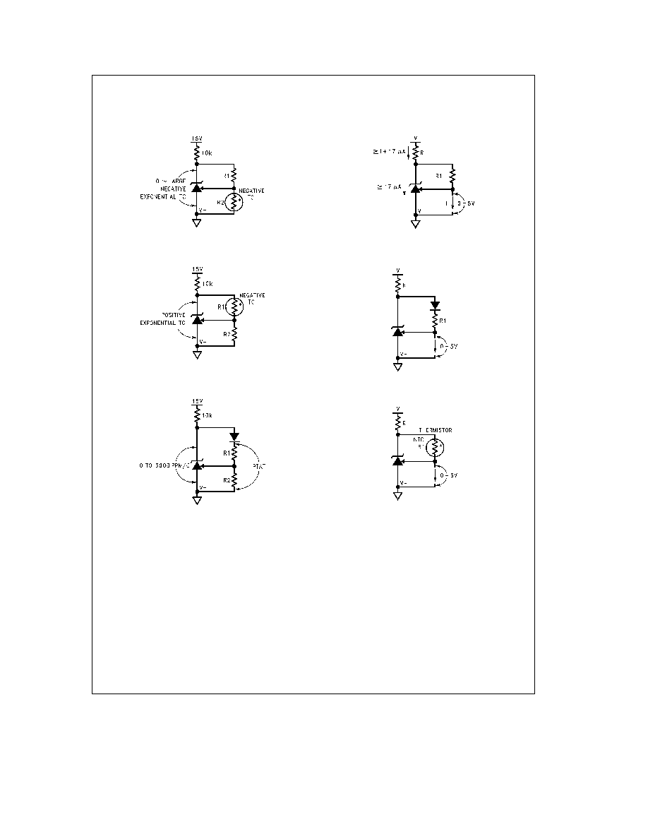
FIGURE 6 Output Voltage has Negative Temperature
Coefficient (TC) if R2 has Negative TC
TL H 11057 � 15
FIGURE 7 Output Voltage has Positive TC
if R1 has Negative TC
TL H 11057 � 16
FIGURE 8 Diode in Series with R1 Causes Voltage
Across R1 and R2 to be Proportional to Absolute
Temperature (PTAT)
Connecting a resistor across V
RO
-to-FEEDBACK creates a
0 TC current source but a range of TCs may be synthe-
sized
TL H 11057 � 17
I
e
V
r
R1
e
1 24 R1
FIGURE 9 Current Source is Programmed by R1
TL H 11057 � 18
FIGURE 10 Proportional-to-Absolute-Temperature
Current Source
TL H 11057 � 19
FIGURE 11 Negative-TC Current Source
Reference Hysteresis
The reference voltage depends slightly on the thermal his-
tory of the die Competitive micro-power products vary
al-
ways check the data sheet for any given device Do not
assume that no specification means no hysteresis
9
Application Information
(Continued)
COMPARATORS
Any of the comparators or the reference may be biased in
any way with no effect on the other sections of the LM615
except when a substrate diode conducts (see Electrical
Characteristics Note 3) For example one or both inputs of
one comparator may be outside the input voltage range lim-
its the reference may be unpowered and the other compar-
ators will still operate correctly Unused comparators should
have inverting input and output tied to V
b
and non-inverting
input tied to V
a
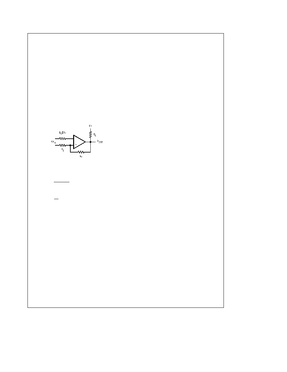
Hysteresis
Any comparator may oscillate or produce a noisy output if
the applied differential input voltage is near the compara-
tor's offset voltage This usually happens when the input
signal is moving very slowly across the comparator's switch-
ing threshold This problem can be prevented by the addi-
tion of hysteresis or positive feedback as shown in
Figure
12
TL H 11057 � 20
FIGURE 12 R
S
and R
F
Add Hysteresis to Comparator
The amount of hysteresis added in
Figure 12 is
V
H
e
V
a
x
R
S
(R
F
a
R
S
)
V
a
x
R
S
R
F
for R
F
n
R
S
A good rule of thumb is to add hysteresis of at least the
maximum specified offset voltage More than about 50 mV
of hysteresis can substantially reduce the accuracy of the
comparator since the offset voltage is effectively being in-
creased by the hysteresis when the comparator output is
high
It is often a good idea to decrease the amount of hysteresis
until oscillations are observed then use three times that
minimum hysteresis in the final circuit Note that the amount
of hysteresis needed is greatly affected by layout The
amount of hysteresis should be rechecked each time the
layout is changed such as changing from a breadboard to a
P C board
Input Stage
The input stage uses lateral PNP input transistors which
unlike those of many op amps have breakdown voltage
BV
EBO
equal to the absolute maximum supply voltage Also
they have no diode clamps to the positive supply nor across
the inputs These features make the inputs look like high
impedances to input sources producing large differential
and common-mode voltages
The guaranteed common-mode input voltage range for an
LM615 is V
b
s
V
CM
s
(V
a
b
1 8V) over temperature
This is the voltage range in which the comparisons must be
made If both inputs are within this range the output will be
at the correct state If one input is within this range and the
other input is less than (V
b
a
32V) even if this is greater
than V
a
the output will be at the correct state If however
either or both inputs are driven below V
b
and either input
current exceeds 10 mA the output state is not guaranteed
to be correct If both inputs are above (V
a
b
1 8V) the
output state is also not guaranteed to be correct
Output Stage
The comparators have open-collector output stages which
require a pull-up resistor from each output pin to a positive
supply voltage of the output to switch properly When the
internal output transistor is off the output (HIGH) voltage
will be pulled up to this external positive voltage
To ensure that the LOW output voltage is under the TTL-low
threshold the output transistor's load current must be less
than 0 8 mA (over temperature) when it turns on This im-
pacts the minimum value of the pull-up resistor
10
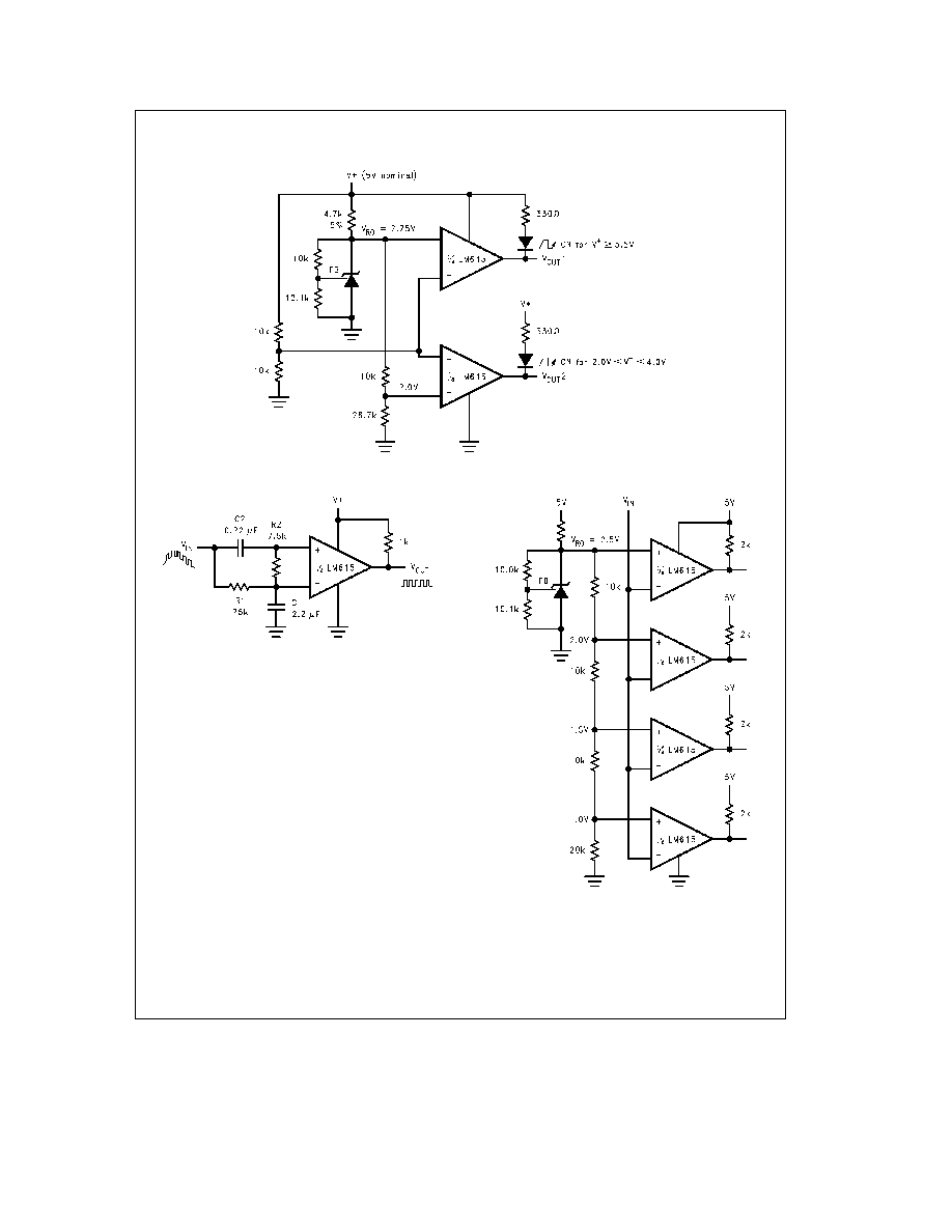
Typical Applications
Power Supply Monitor
TL H 11057 � 21
V
OUT1
and V
OUT2
are optional digital
outputs and are LOW when the
corresponding LED is ON
All resistors 1%
tolerance or better
Tracking Comparator
TL H 11057 � 22
R1�C1 removes the low-frequency signal component
so that through R2�C2 the higher-
frequency component is detected
4-Threshold Level Detector
TL H 11057 � 23
11

12
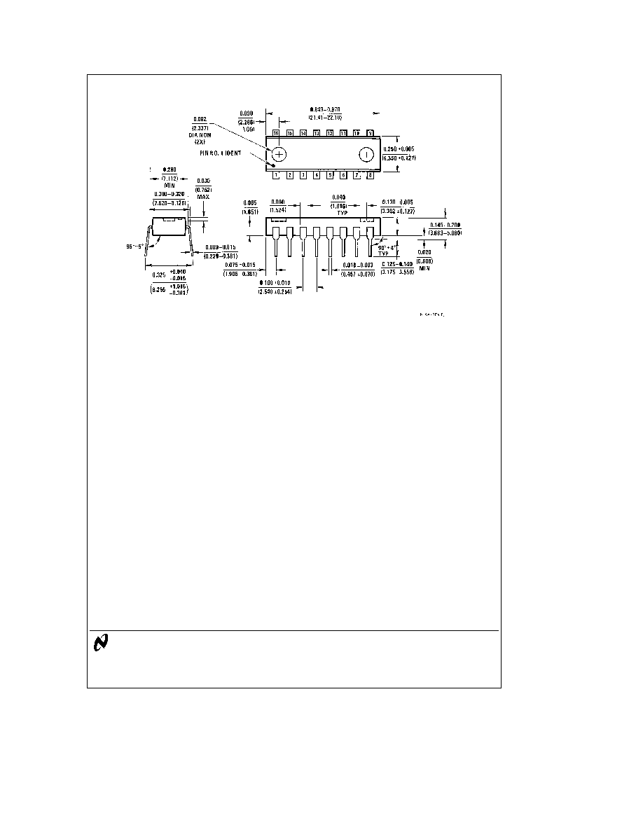
Physical Dimensions
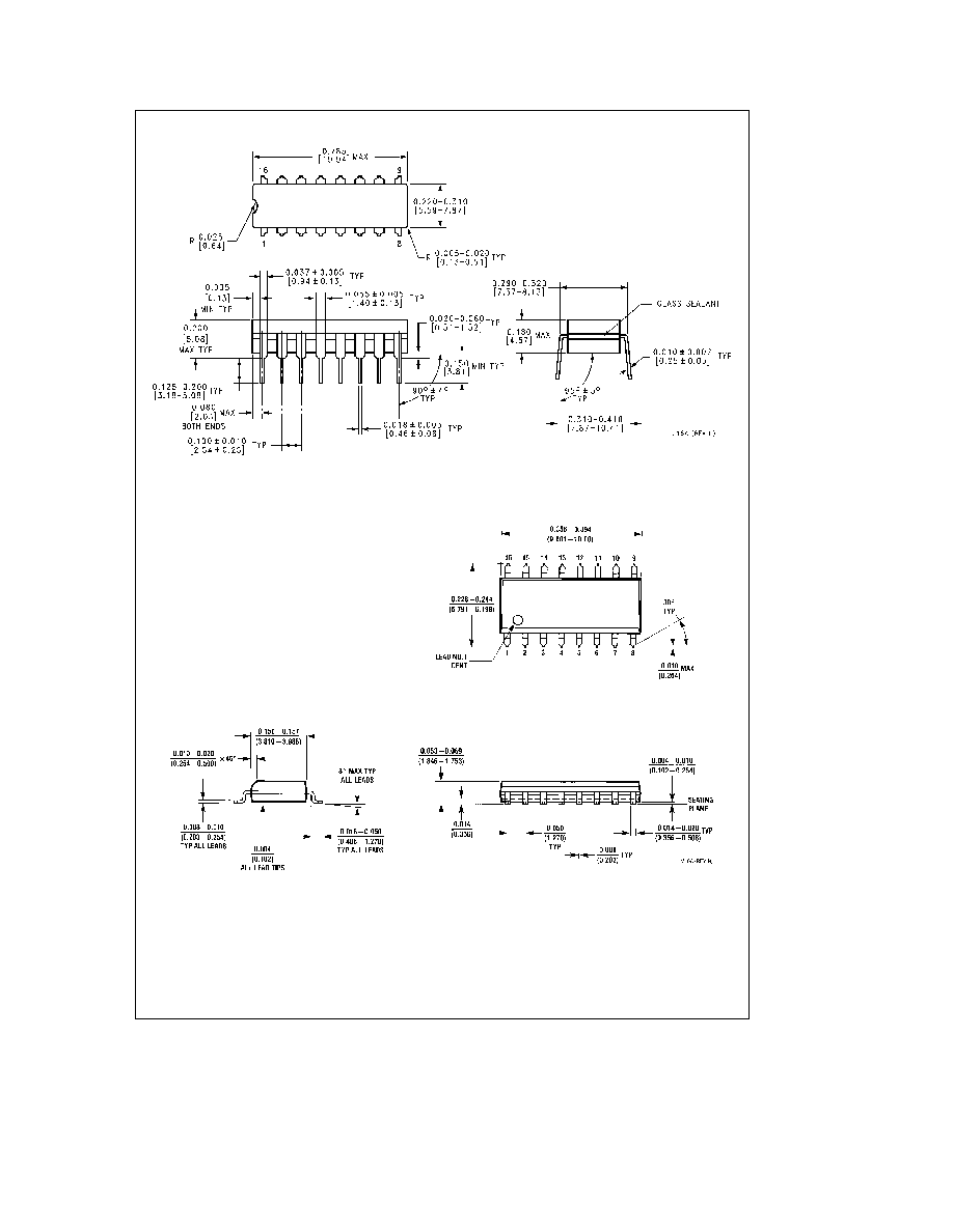
inches (millimeters)
Ceramic Dual-In-Line Package (J)
Order Number LM615AMJ 883
NS Package Number J16A
16-Pin Narrow Surface Mount Package (M)
Order Number LM615IM
NS Package Number M16A
13
LM615
Quad
Comparator
and
Adjustable
Reference
Physical Dimensions
inches (millimeters) (Continued)
16-Pin Molded Dual-In-Line Package (N)
Order Number LM615IN or LM615MN
NS Package Number N16A
LIFE SUPPORT POLICY
NATIONAL'S PRODUCTS ARE NOT AUTHORIZED FOR USE AS CRITICAL COMPONENTS IN LIFE SUPPORT
DEVICES OR SYSTEMS WITHOUT THE EXPRESS WRITTEN APPROVAL OF THE PRESIDENT OF NATIONAL
SEMICONDUCTOR CORPORATION As used herein
1 Life support devices or systems are devices or
2 A critical component is any component of a life
systems which (a) are intended for surgical implant
support device or system whose failure to perform can
into the body or (b) support or sustain life and whose
be reasonably expected to cause the failure of the life
failure to perform when properly used in accordance
support device or system or to affect its safety or
with instructions for use provided in the labeling can
effectiveness
be reasonably expected to result in a significant injury
to the user
National Semiconductor
National Semiconductor
National Semiconductor
National Semiconductor
Corporation
Europe
Hong Kong Ltd
Japan Ltd
1111 West Bardin Road
Fax (a49) 0-180-530 85 86
13th Floor Straight Block
Tel 81-043-299-2309
Arlington TX 76017
Email cnjwge tevm2 nsc com
Ocean Centre 5 Canton Rd
Fax 81-043-299-2408
Tel 1(800) 272-9959
Deutsch Tel (a49) 0-180-530 85 85
Tsimshatsui Kowloon
Fax 1(800) 737-7018
English
Tel (a49) 0-180-532 78 32
Hong Kong
Fran ais Tel (a49) 0-180-532 93 58
Tel (852) 2737-1600
Italiano
Tel (a49) 0-180-534 16 80
Fax (852) 2736-9960
National does not assume any responsibility for use of any circuitry described no circuit patent licenses are implied and National reserves the right at any time without notice to change said circuitry and specifications