LM6162
High Speed Operational Amplifier
General Description
The LM6162 family of high-speed amplifiers exhibits an ex-
cellent speed-power product, delivering 300 V/µs and
100 MHz gain-bandwidth product (stable for gains as low as
+2 or -1) with only 5 mA of supply current. Further power
savings and application convenience are possible by taking
advantage of the wide dynamic range in operating supply
voltage which extends all the way down to +5V.
These amplifiers are built with National's VIP
TM
(Vertically In-
tegrated PNP) process which provides fast transistors that
are true complements to the already fast NPN devices. This
advanced junction-isolated process delivers high speed per-
formance without the need for complex and expensive di-
electric isolation.
Features
n
High slew rate:
300 V/µs
n
High gain-bandwidth product:
100 MHz
n
Low supply current:
5 mA
n
Fast settling time:
120 ns to 0.1%
n
Low differential gain:
<
0.1%
n
Low differential phase:
<
0.1∞
n
Wide supply range:
4.75V to 32V
n
Stable with unlimited capacitive load
n
Well behaved; easy to apply
Applications
n
Video amplifier
n
Wide-bandwidth signal conditioning for image
processing (FAX, scanners, laser printers)
n
Hard disk drive preamplifier
n
Error amplifier for high-speed switching regulator
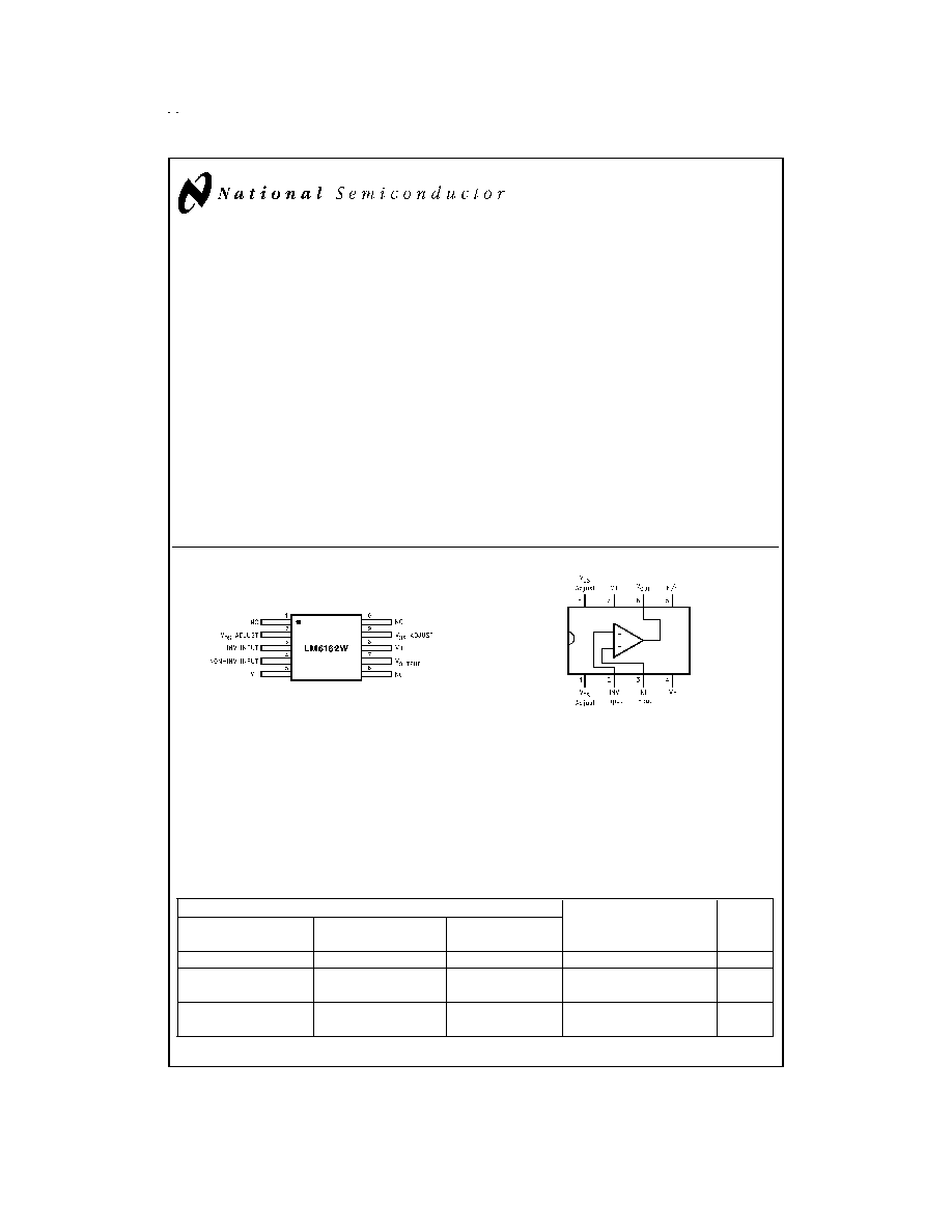
Connection Diagrams
Temperature Range
Package
NSC
Drawing
Military
Industrial
Commercial
-55∞C
T
A
+125∞C
-25∞C
T
A
+85∞C
0∞C
T
A
+70∞C
LM6162N
8-Pin Molded DIP
N08E
LM6162J/883
8-Pin Ceramic DIP
J08A
5962-9216501PA
LM6162WG/883
10-Lead Ceramic SOIC
WG10A
5962-9216501XA
VIP
TM
is a trademark of National Semiconductor Corporation.
10-Pin Ceramic Flatpak
DS011061-15
Top View
See NS Package Number W10A
DS011061-2
See NS Package Number N08E or J08A
May 1999
LM6162
High
Speed
Operational
Amplifier
© 1999 National Semiconductor Corporation
DS011061
www.national.com
Connection Diagrams
(Continued)
Temperature Range
Package
NSC
Drawing
Military
Industrial
Commercial
-55∞C
T
A
+125∞C
-25∞C
T
A
+85∞C
0∞C
T
A
+70∞C
LM6162W/883
10-Pin Ceramic Flatpak
W10A
5962-9216501HA
www.national.com
2
Absolute Maximum Ratings
(Note 1)
If Military/Aerospace specified devices are required,
please contact the National Semiconductor Sales Office/
Distributors for availability and specifications.
Supply Voltage (V
+
≠V
-
)
36V
Differential Input Voltage (Note 2)
±
8V
Common-Mode Input Voltage
(V
+
-0.7V) to
(Note 3)
(V
-
+ 0.7V)
Output Short Circuit to GND
(Note 4)
Continuous
Soldering Information
Dual-In-Line Package (N)
Soldering (10 seconds)
260∞C
Small Outline Package (M)
Vapor Phase (60 seconds)
Infrared (15 seconds)
215∞C
220∞C
See AN-450 "Surface Mounting Methods and Their Effect
on Product Reliability" for other methods of soldering
surface mount devices.
Storage Temperature Range
-65∞C
T
J
+150∞C
Max Junction Temperature
150∞C
ESD Tolerance (Note 5)
±
1100V
Operating Ratings
Temperature Range (Note 6)
LM6162
-55∞C
T
J
+125∞C
Supply Voltage Range
4.75V to 32V
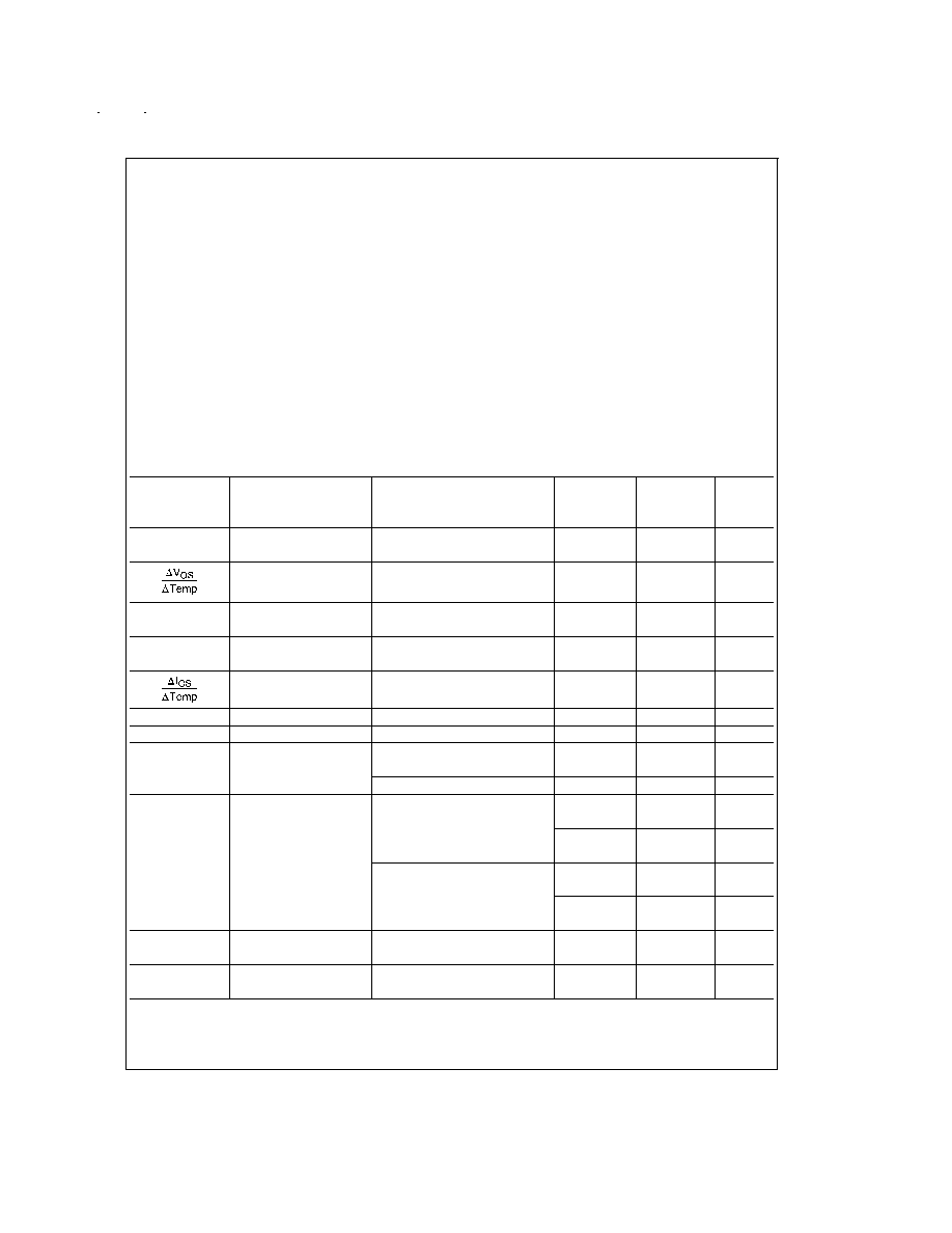
DC Electrical Characteristics
These limits apply for supply voltage =
±
15V, V
CM
= 0V, and R
L
100 k
, unless otherwise specified. Limits in standard
typeface are for T
A
= T
J
= 25∞C; limits in boldface type apply over the Operating Temperature Range.
Typical
(Note 7)
LM6162
Symbol
Parameter
Conditions
Limit
Units
(Note 8)
V
OS
Input Offset Voltage
±
3
±
5
mV
±
8
max
Input Offset Voltage
7
µV/∞C
Average Drift
I
bias
Input Bias Current
2.2
3
µA
6
max
I
OS
Input Offset Current
±
150
±
350
nA
±
800
max
Input Offset Current
0.3
nA/∞C
Average Drift
R
IN
Input Resistance
Differential
180
k
C
IN
Input Capacitance
2.0
pF
A
VOL
Large Signal
V
OUT
=
±
10V, R
L
= 2 k
1400
1000
V/V
Voltage Gain
(Note 9)
500
min
R
L
= 10 k
6500
V/V
V
CM
Input Common-Mode
Supply =
±
15V
+14.0
+13.9
V
Voltage Range
+13.8
min
-13.2
-12.9
V
-12.7
max
Supply = +5V
4.0
3.9
V
(Note 10)
3.8
min
1.6
1.8
V
2.0
max
CMRR
Common-Mode
-10V
V
CM
+10V
100
83
dB
Rejection Ratio
79
min
PSRR
Power Supply
±
10V
V
S
±
16V
93
83
dB
Rejection Ratio
79
min
www.national.com
3
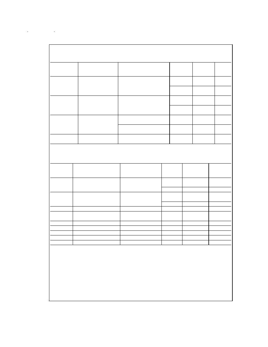
DC Electrical Characteristics
(Continued)
These limits apply for supply voltage =
±
15V, V
CM
= 0V, and R
L
100 k
, unless otherwise specified. Limits in standard
typeface are for T
A
= T
J
= 25∞C; limits in boldface type apply over the Operating Temperature Range.
Typical
(Note 7)
LM6162
Symbol
Parameter
Conditions
Limit
Units
(Note 8)
V
O
Output Voltage
Supply =
±
15V, R
L
= 2 k
+14.2
+13.5
V
Swing
+13.3
min
-13.4
-13.0
V
-12.7
max
V
O
Output Voltage Swing
Supply = +5V and
4.2
3.5
V
R
L
= 2 k
(Note 10)
3.3
min
1.3
1.7
V
2.0
max
I
OSC
Output Short
Sourcing
65
30
mA
Circuit Current
20
min
Sinking
65
30
mA
20
min
I
S
Supply Current
5.0
6.5
mA
6.8
max
AC Electrical Characteristics
These limits apply for supply voltage =
±
15V, V
CM
= 0V, R
L
100 k
, and C
L
5 pF, unless otherwise specified. Limits
in standard typeface are for T
A
= T
J
= 25∞C; limits in boldface type apply over the Operating Temperature Range.
Typical
(Note
7)
LM6162
Symbol
Parameter
Conditions
Limit
Units
(Note 8)
GBW
Gain-Bandwidth Product
f = 20 MHz
100
80
MHz
55
min
Supply =
±
5V
70
MHz
SR
Slew Rate
A
V
= +2 (Note 11)
300
200
V/µs
180
min
Supply =
±
5V
200
V/µs
PBW
Power Bandwidth
V
OUT
= 20 V
PP
4.5
MHz
t
s
Settling Time
10V step, to 0.1%
100
ns
A
V
= -1, R
L
= 2 k
m
Phase Margin
A
V
= +2
45
deg
Differential Gain
NTSC, A
V
= +2
<
0.1
%
Differential Phase
NTSC, A
V
= +2
<
0.1
deg
e
n
Input Noise Voltage
f = 10 kHz
10
nV/
Hz
i
n
Input Noise Current
f = 10 kHz
1.2
pA/
Hz
Note 1: Absolute maximum ratings indicate limits beyond which damage to the component may occur. Electrical specifications do not apply when operating the de-
vice beyond its rated operating conditions.
Note 2: The ESD protection circuitry between the inputs will begin to conduct when the differential input voltage reaches 8V.
Note 3: a) In addition, the voltage between the V
+
pin and either input pin must not exceed 36V.
b) When the voltage applied to an input pin is driven more than 3V below the negative supply pin voltage, a substrate diode begins to conduct. Current through this
pin must then be kept less than 20 mA to limit damage from self-heating.
Note 4: Although the output current is internally limited, continuous short-circuit operation at elevated ambient temperature can result in exceeding the maximum al-
lowed junction temperature of 150∞C.
Note 5: This value is the average voltage that the weakest pin combinations can withstand and still conform to the datasheet limits. The test circuit used consists
of the human body model, 100 pF in series with 1500
.
Note 6: The typical thermal resistance, junction-to-ambient, of the molded plastic DIP (N package) is 105∞C/W. For the molded plastic SO (M package), use
155∞C/W. All numbers apply for packages soldered directly into a printed circuit board.
Note 7: Typical values are for T
J
= 25∞C, and represent the most likely parametric norm.
Note 8: Limits are guaranteed, by testing or correlation.
www.national.com
4
AC Electrical Characteristics
(Continued)
Note 9: Voltage Gain is the total output swing (20V) divided by the magnitude of the input signal required to produce that swing.
Note 10: For single-supply operation, the following conditions apply: V
+
= 5V, V
-
= 0V, V
CM
= 2.5V, V
OUT
= 2.5V. Pin 1 and Pin 8 (V
OS
Adjust pins) are each con-
nected to pin 4 (V
-
) to realize maximum output swing. This connection will increase the offset voltage.
Note 11: V
IN
= 10V step. For
±
5V supplies, V
IN
= 1V step.
Note 12: A military RETS electrical test specification is available on request.
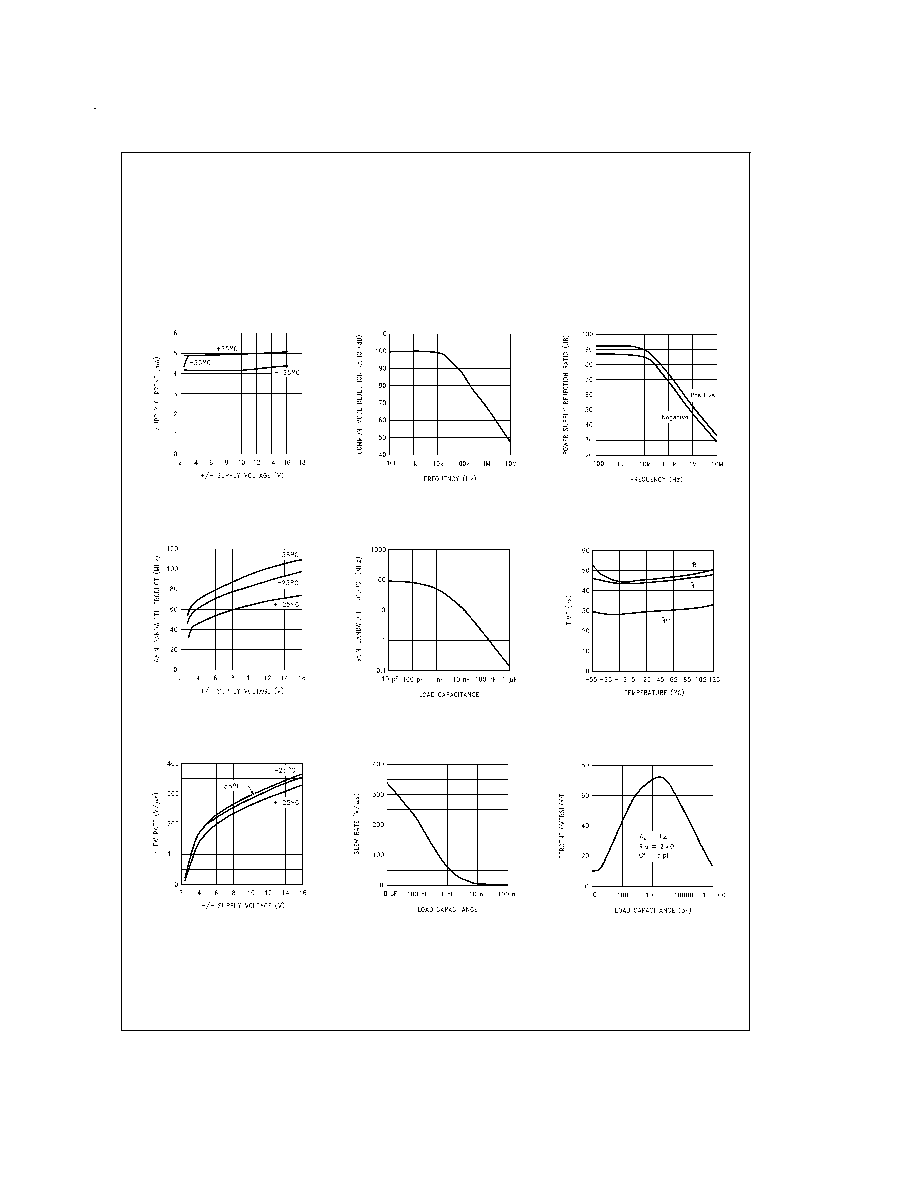
Typical Performance Characteristics
R
L
= 10 k
, T
A
= 25∞C unless otherwise noted
Supply Current vs
Supply Voltage
DS011061-16
Common-Mode
Rejection Ratio
DS011061-17
Power Supply
Rejection Ratio
DS011061-18
Gain-Bandwidth Product
vs Supply Voltage
DS011061-19
Gain-Bandwidth Product
vs Load Capacitance
DS011061-20
Propagation Delay,
Rise and Fall Times
DS011061-21
Slew Rate vs
Supply Voltage
DS011061-22
Slew Rate vs
Load Capacitance
DS011061-23
Overshoot vs
Load Capacitance
DS011061-24
www.national.com
5