 | –≠–ª–µ–∫—Ç—Ä–æ–Ω–Ω—ã–π –∫–æ–º–ø–æ–Ω–µ–Ω—Ç: LM621 | –°–∫–∞—á–∞—Ç—å:  PDF PDF  ZIP ZIP |
TL H 8679
LM621
Brushless
Motor
Commutator
August 1992
LM621 Brushless Motor Commutator
General Description
The LM621 is a bipolar IC designed for commutation of
brushless DC motors The part is compatible with both
three- and four-phase motors It can directly drive the power
switching devices used to drive the motor The LM621 pro-
vides an adjustable dead-time circuit to eliminate ``shoot-
through'' current spiking in the power switching circuitry
Operation is from a 5V supply but output swings of up to
40V are accommodated The part is packaged in an 18-pin
dual-in-line package
Features
Y
Adjustable dead-time feature eliminates current spiking
Y
On-chip clock oscillator for dead-time feature
Y
Outputs drive bipolar power devices (up to 35 mA base
current) or MOSFET power devices
Y
Compatible with three- and four-phase motors
Bipolar drive to delta- or Y-wound motors
Unipolar drive to center-tapped Y-wound motors
Supports 30- and 60-degree shaft position sensor
placements for three-phase motors
Supports 90-degree sensor placement for four-phase
motors
Y
Directly interfaces to pulse-width modulator output(s)
via OUTPUT INHIBIT (PWM magnitude) and DIREC-
TION (PWM sign) inputs
Y
Direct interface to Hall sensors
Y
Outputs are current limited
Y
Undervoltage lockout
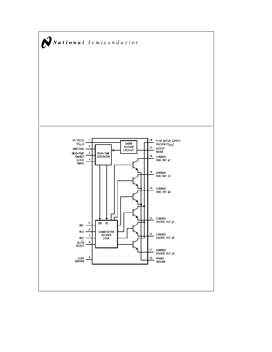
Connection Diagram
TL H 8679 ≠ 1
Order Number LM621N
See NS Package Number N18A
C1995 National Semiconductor Corporation
RRD-B30M115 Printed in U S A
Absolute Maximum Ratings
(See Notes)
If Military Aerospace specified devices are required
please contact the National Semiconductor Sales
Office Distributors for availability and specifications
V
CC1
a
7V
V
CC2
a
45V
Logic Inputs (Note 1)
V
CC1
a
0 5V
b
0 5V
Logic Input Clamp Current
20 mA
Output Voltages
a
45V
b
0 5V
Output Currents
Internally current limited
Operating Ambient Temperature Range
LM621
b
40 C to
a
85 C
Storage Temperature Range
b
65 C to
a
150 C
Junction Temperature
150 C
ESD Susceptibility (Note 10)
2000V
Lead Temperature N pkg
(Soldering 4 sec )
260 C
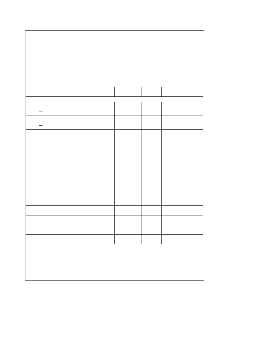
Electrical Characteristics
(See Notes)
Parameter
Conditions
Typ
Tested
Design
Units
Limits
Limits
DECODER SECTION
High Level Input Voltage
HS1 HS2 HS3
2 0
2 0
V min
30 60 SELECT
2 0
2 0
V min
High Level Input Current
HS1 HS2 HS3
V
IH
e
V
CC1
100
200
m
A max
30 60 SELECT
V
IH
e
V
CC1
120
240
m
A max
Low Level Input Voltage
HS1 HS3 and HS2
30 60
e
5V
0 6
0 4
V max
HS1 HS3 and HS2
30 60
e
0V
0 6
0 4
V max
30 60 Select
H
SI
e
H
S3
e
5V
0 6
0 4
V
max
Low Level Input Current
HS1 and HS3
V
IL
e
0 35V
b
400
b
600
m
A max
HS2
V
IL
e
0 4V
b
100
b
200
m
A max
30 60 SELECT
V
IL
e
0 0V
b
700
b
1000
m
A max
Input Clamp Voltage
I
in
e
1 mA
(V
CC1
a
0 7)
V
(Pins 2 3 5 6 7 8 17)
I
in
e b
1 mA
(
b
0 6)
V
Output Leakage Current
Outputs Off
Sinking Outputs
V
CC2
e
40V
0 2
1 0
m
A
V
OUT
e
40V
Sourcing Outputs
V
OUT
e
0V
b
0 2
b
1 0
m
A
Short-Circuit Current
V
CC2
e
10V
50
35
mA min
Sinking Outputs
V
OUT
e
10V
Sourcing Outputs
V
OUT
e
0V
b
50
b
35
mA min
V
sat
(sinking)
I
e
20 mA
0 83
1 00
V max
V
drop
(sourcing)
e
(V
CC2
b
V
OUT
)
I
e b
20 mA
1 7
2 00
V max
Output Rise Time
(sourcing)
50
ns
C
L
k
10 pF
Output Fall Time
(sinking)
50
ns
C
L
s
10 pF
Propagation Delay
Dead-Time Off
200
ns
(Hall Input to Output)
2

Electrical Characteristics
(See Notes) (Continued)
Parameter
Conditions
Typ
Tested
Design
Units
Limits
Limits
DEAD-TIME SECTION
High Level Input Voltage
DIRECTION
Pin 3
e
0V
2 0
2 0
V min
OUTPUT INHIBIT
2 0
2 0
V min
DEAD-TIME ENABLE
Pin 17
e
0V
2 0
2 0
V min
High Level Input Current
V
in
e
5V
DIRECTION
Pin 3
e
0V
100
150
m
A max
OUTPUT INHIBIT
60
100
m
A max
DEAD-TIME ENABLE
200
300
m
A max
Low Level Input Voltage
DIRECTION
Pin 3
e
0V
0 6
0 4
V max
OUTPUT INHIBIT
0 6
0 4
V max
DEAD-TIME ENABLE
0 3
0 2
V max
Low Level Input Current
DIRECTION
V
in
e
0 6V
b
100
b
150
m
A max
OUTPUT INHIBIT
V
in
e
0 6V
b
60
b
100
m
A max
DEAD-TIME ENABLE
V
in
e
0V
b
200
b
300
m
A max
Propagation Delays
Dead-Time Off
(Inputs to Outputs)
(Pin 3
e
0V)
OUTPUT INHIBIT
200
ns
DIRECTION
200
ns
Minimum Clock Period
R
e
11 kX R
1
e
1k
1 8
m
s
T
CLK
(Notes 3 11)
C
e
200 pF
Clock Accuracy
R
e
30k R
1
e
1k
g
3
%
f
e
100 kHz (Note 11)
C
e
420 pF
Minimum Dead-Time
Dead-Time Off
15
ns
Minimum Dead-Time
Dead-Time On
2
T
CLK
COMPLETE CIRCUIT
Total Current Drains
Outputs Off
I
CC1
10
mA min
I
CC1
15
22
30
mA max
I
CC2
V
CC2
e
40V
2
mA min
I
CC2
3
6
9
mA max
Undervoltage Lockout
3 6
3 0
V
MAX
V
CC1
Note 1
Unless otherwise noted ambient temperature (T
A
)
e
25 C
Note 2
Unless otherwise noted V
CC1
e a
5 0V ``recommended operating range V
CC
e
4 5V to 5 5V'' V
CC2
e a
10 0V ambient temperature
e
25 C
Note 3
The clock period is typically T
CLK
e
(0 756
c
10
b
3
) (R
a
1) C where T
CLK
is in ms R is in kX and C is pF Also see selection graph in Typical
Characteristics for determining values of R and C Note that the value of R should be no less than 11 kX and C no less than 200 pF
Note 4
Tested limits are guaranteed and 100% production tested
Note 5
Design limits are guaranteed (but not 100% production tested) at the indicated temperature and supply voltages These limits are not used to calculate
outgoing quality levels
Note 6
Specifications in boldface apply over junction temperature range of
b
40 C to
a
85 C
Note 7
Typical Thermal Resistances
O
JA
(see Note 8)
N pkg board mounted
110 C W
N pkg socketed
118 C W
Note 8
Package thermal resistance indicates the ability of the package to dissipate heat generated on the die Given ambient temperature and power dissipation
the thermal resistance parameter can be used to determine the approximate operating junction temperature Operating junction temperature directly effects
product performance and reliability
Note 9
This part specifically does not have thermal shutdown protection to avoid safety problems related to an unintentional restart due to thermal time constant
variations Care should be taken to prevent excessive power dissipation on the die
Note 10
Human body model 100 pF discharged through a 1500X resistor
Note 11
R
1
e
0 for C
t
620 pF
3
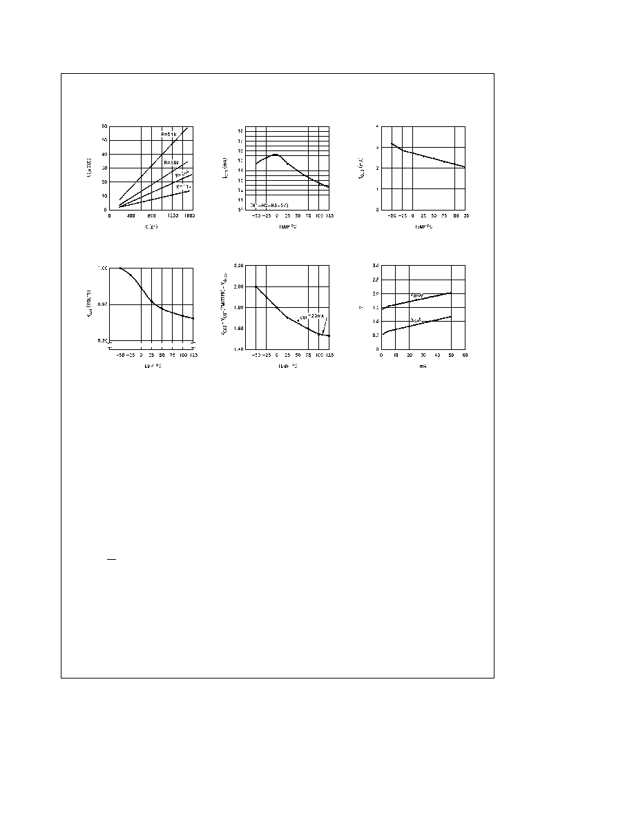
Typical Performance Characteristics
for R and C
Selection Graph
vs Temperature
Supply Currents
vs Temperature
Supply Currents
V
sat
vs Temperature
V
drop
vs Temperature
(
T
A
e
25 C)
Typ V
drop
vs I
out source
Typ V
sat
vs I
out sink
TL H 8679 ≠ 2
Description of Inputs and Outputs
Pin 1 V
CC1
(
a
5V)
The logic and clock power supply pin
Pin 2 DIRECTION
This input determines the direction of
rotation of the motor ie
clockwise vs counterclockwise
See truth table
Pin 3 DEAD-TIME ENABLE
This input enables or disables
the dead-time feature Connecting
a
5V to pin 3 enables
dead-time and grounding pin 3 disables it Pin 3 should not
be allowed to float
Pin 4 CLOCK TIMING
An RC network connected between
this pin and ground sets the period of the clock oscillator
which determines the amount of dead-time See
Figure 2
and text
Pins 5 thru 7 HS1 HS2 and HS3 (Hall-sensor inputs)
These inputs receive the rotor-position sensor inputs from
the motor Three-phase motors provide all three signals
four phase motors provide only two one of which is con-
nected to both HS2 and HS3
Pin 8 30 60 SELECT
This input is used to select the re-
quired decoding for three-phase motors ie either ``30-de-
gree'' (
a
5V) or ``60-degree'' (ground) Connect pin 8 to
a
5V when using a four-phase motor
Pin 9 LOGIC GROUND
Ground for the logic power supply
Pin 10 POWER GROUND
Ground for the output buffer
supply
Pins 11 thru 13 SOURCE OUTPUTS
The three current-
sourcing outputs which drive the external power devices
that drive the motor
Pins 14 thru 16 SINK OUTPUTS
The three current-sinking
outputs which drive the external power devices that drive
the motor
Pin 17 OUTPUT INHIBIT
This input disables the LM621
outputs It is typically driven by the magnitude signal from an
external sign magnitude PWM generator Pin 17
e a
5V
e
outputs off
Pin 18 V
CC2
(
a
5 to
a
40V)
This is the supply for the
collectors of the three current-sourcing outputs (pins 11 thru
13) When driving MOSFET power devices pin 18 may be
connected to a voltage source of up to
a
40V to achieve
sufficient output swing for the gate When driving bipolar
power devices pin 18 should be connected to
a
5V to mini-
mize on-chip power dissipation Undervoltage lockout auto-
matically shuts down all outputs if the V
CC1
supply is too
low All outputs will be off if V
CC1
falls below the undervol-
tage lockout voltage
4
Functional Description
The commutation decoder receives Hall-sensor inputs HS1
HS2 and HS3 and a 30 60 SELECT input This block de-
codes the gray-code sequence to the required motor-drive
sequence
The dead-time generator monitors the DIRECTION input
and inhibits the outputs (pins 11 thru 16) for a time sufficient
to prevent current-spiking in the external power switches
when the direction is reversed
The six chip outputs drive external power switching devices
which drive the motor Three outputs source current the
remaining three sink current The output transistors provide
up to 50 mA outputs for driving devices or up to 40V output
swings for driving MOSFETs The LM621 logic is powered
from 5V
The undervoltage lockout section monitors the V
CC
supply
and if the voltage is not sufficient to permit reliable logic
operation the outputs are shutdown
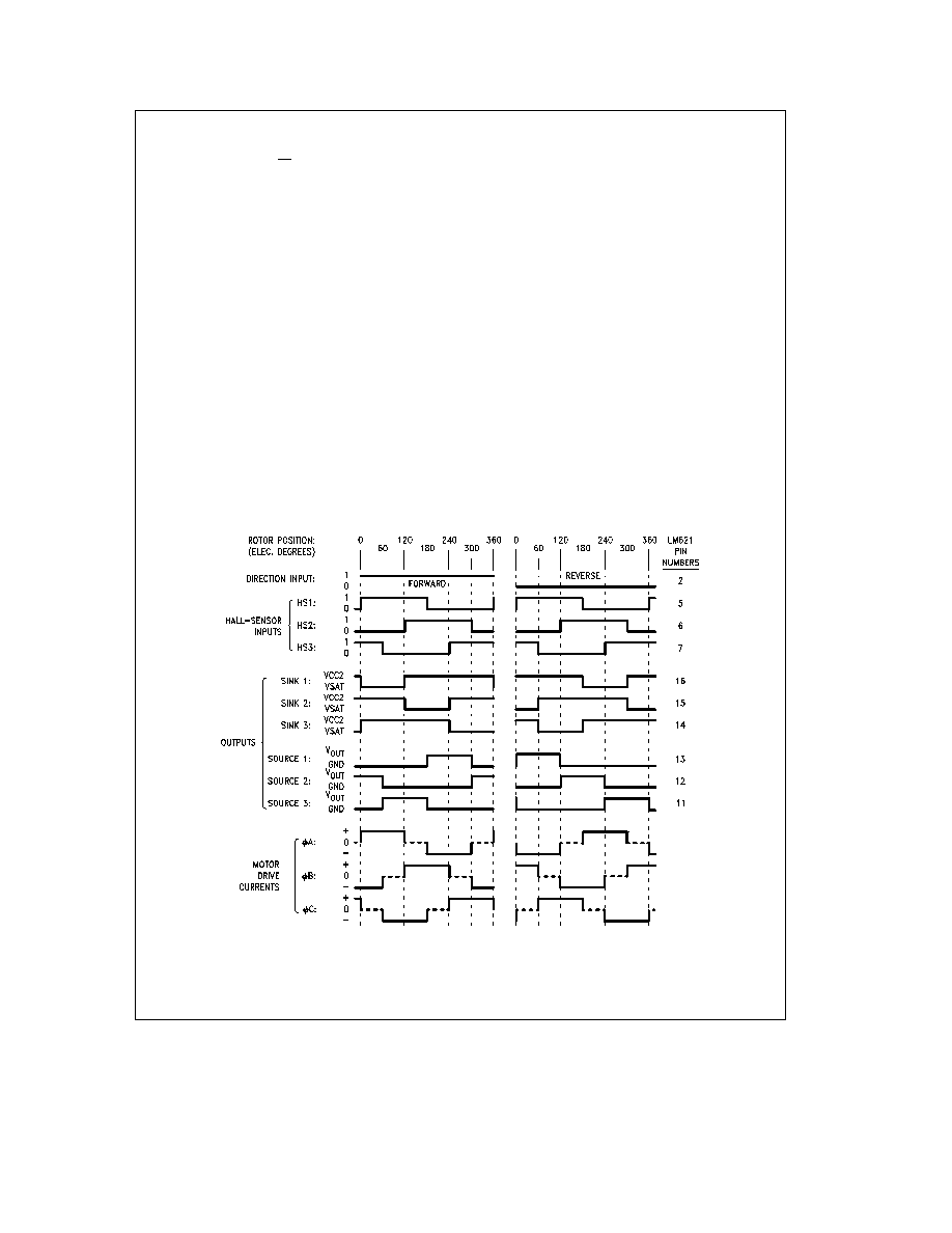
Three-Phase Motor Commutation
There are two popular conventions for establishing the rela-
tive phasing of rotor-position signals for three-phase mo-
tors While usually referred to as 30-degree and 60-degree
sensor placements this terminology refers to mechanical
degrees of sensor placement not electrical degrees The
electrical angular resolution is the required 60 degrees in
both cases The phasing differences can be noted by com-
paring the sequences of HS1 through HS3 entries in Table I
LM621 Commutation Decoder Truth Table which shows
both the 30- and 60-degree phasings (and the 90-degree
phasing for four-phase motors) and their required decoder
logic truth tables respectively Table I shows the phasing
(or codes) of the Hall-effect sensors for each 60-degree
(electrical) position range of the rotor and correlates these
data to the commutator sink and source outputs required to
drive the power switches These phasings are common to
several motor manufacturers The 60-degree phasing is pre-
ferred to 30-degree phasing because the all-zeros and all-
ones codes are not generated The 60-degree phasing is
more failsafe because the all-zeros and all-ones codes
could be inadvertently generated by things like disconnect-
ed or shorted sensors
Because the above terminology is not used consistently
among all motor manufacturers Table II Alternative Sen-
sor-phasing Names will hopefully clarify some of the differ-
ences Table II shows a different 60-degree phasing and
120- 240- and 300-degree phasings Comparison with Ta-
ble I will show that these four phasings are essentially shift-
ed and or reversed-order versions of those used with the
LM621
Figure 1 shows the waveforms associated with the commu-
tation decoder logic for a motor which has 60-degree rotor-
position phasing along with the generated motor-drive
waveforms As can be seen in the drawing Hall-effect sen-
sor signals HS1 through HS3 are separated by 60 electrical
degrees which is the required angular resolution for three-
phase motors
TL H 8679 ≠ 6
FIGURE 1 Commutation Waveforms for 60-degree Phasing
5