 | –≠–ª–µ–∫—Ç—Ä–æ–Ω–Ω—ã–π –∫–æ–º–ø–æ–Ω–µ–Ω—Ç: LM6218AN | –°–∫–∞—á–∞—Ç—å:  PDF PDF  ZIP ZIP |
LM6118/LM6218
Fast Settling Dual Operational Amplifiers
General Description
The
LM6118/LM6218
are
monolithic
fast-settling
unity-gain-compensated dual operational amplifiers with
±
20
mA output drive capability. The PNP input stage has a typical
bias current of 200 nA, and the operating supply voltage is
±
5V to
±
20V.
These dual op amps use slew enhancement with special
mirror circuitry to achieve fast response and high gain with
low total supply current.
The amplifiers are built on a junction-isolated VIP
TM
(Verti-
cally Integrated PNP) process which produces fast PNP's
that complement the standard NPN's.
Features
Typical
j
Low offset voltage:
0.2 mV
j
0.01% settling time:
400 ns
j
Slew rate A
v
= -1:
140 V/µs
j
Slew rate A
v
= +1:
75 V/µs
j
Gain bandwidth:
17 MHz
j
Total supply current:
5.5 mA
j
Output drives 50
load (
±
1V)
Applications
n
D/A converters
n
Fast integrators
n
Active filters
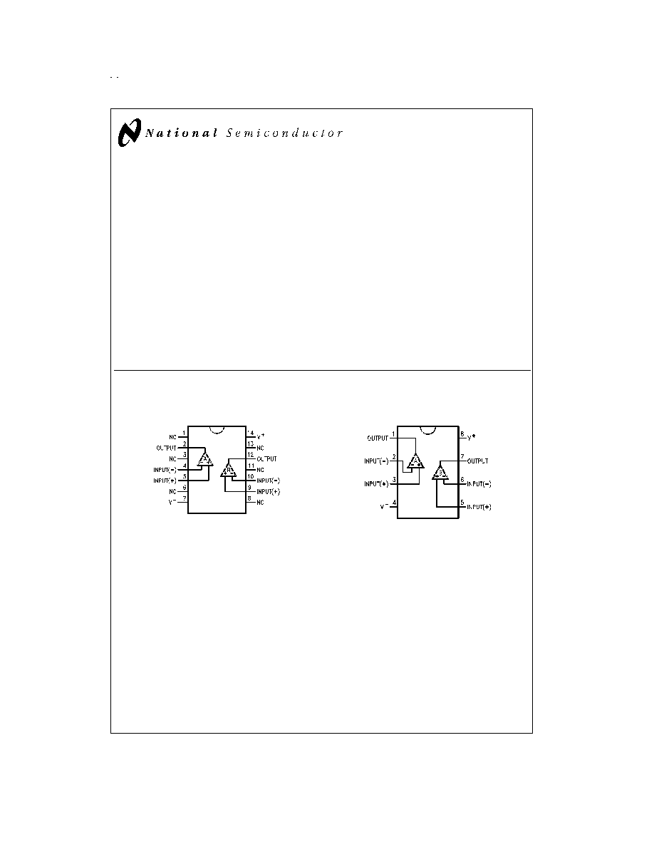
Connection Diagrams and Order Information
VIP
TM
is a trademark of National Semiconductor Corporation.
Small Outline Package (WM)
DS010254-3
Top View
Order Number LM6218WM
See NS Package Number M14B
Dual-In-Line Package (J or N)
DS010254-4
Top View
Order Number LM6118N,
LM6218AN or LM6218N
See NS Package Number N08E
May 1999
LM61
18/LM6218
Fast
Settling
Dual
Operational
Amplifiers
© 1999 National Semiconductor Corporation
DS010254
www.national.com

Typical Applications
DS010254-1
Single ended input to differential output
A
V
= 10, BW = 3.2 MHz
40 V
PP
Response = 1.4 MHz
V
S
=
±
15V
Wide-Band, Fast-Settling
40 V
PP
Amplifier
www.national.com
2
Absolute Maximum Ratings
(Note 1)
If Military/Aerospace specified devices are required,
please contact the National Semiconductor Sales Office/
Distributors for availability and specifications.
Total Supply Voltage
42V
Input Voltage
(Note 2)
Differential Input Current (Note 3)
±
10 mA
Output Current (Note 4)
Internally Limited
Power Dissipation (Note 5)
500 mW
ESD Tolerance
(C = 100 pF, R = 1.5 k
)
±
2 kV
Junction Temperature
150∞C
Storage Temperature Range
-65∞C to +150∞C
Lead Temperature
(Soldering, 10 sec.)
300∞C
Operating Temp. Range
LM6118
-55∞C to +125∞C
LM6218A
-40∞C to +85∞C
LM6218
-40∞C to +85∞C
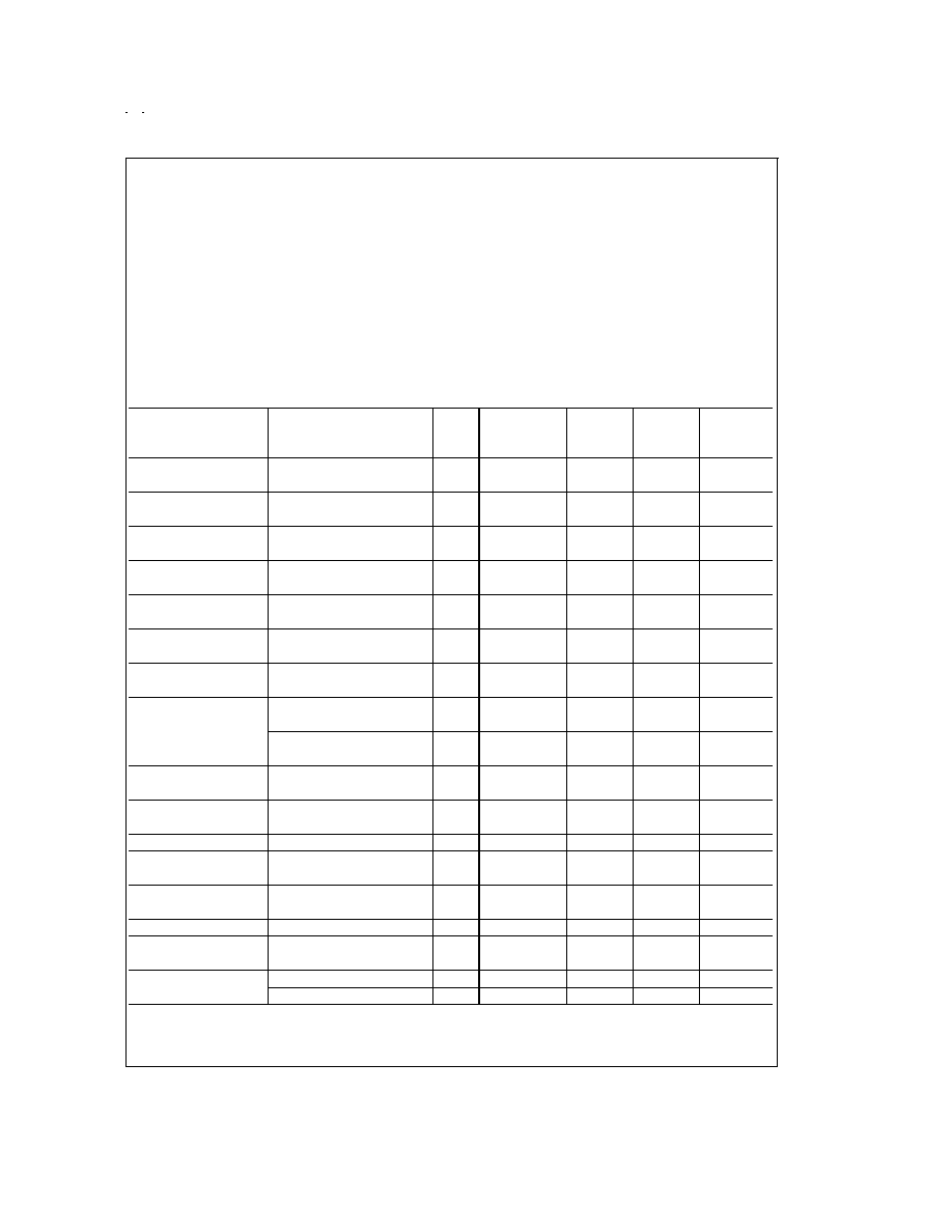
Electrical Characteristics
±
5V
V
S
±
20V, V
CM
= 0V, V
OUT
= 0V, I
OUT
= 0A, unless otherwise specified. Limits with standard type face are for T
J
=
25∞C, and Bold Face Type are for Temperature Extremes.
Typ
LM6118
LM6218A
LM6218
Parameter
Conditions
25∞C
Limits
Limits
Limits
Units
(Note 6)
(Note 6)
(Note 6)
Input Offset Voltage
V
S
=
±
15V
0.2
1
1
3
mV (max)
2
2
4
Input Offset Voltage
V- + 3V
V
CM
V+ - 3.5V
0.3
1.5
1.5
3.5
mV (max)
2.5
2.5
4.5
Input Offset Current
V- + 3V
V
CM
V+ - 3.5V
20
50
50
100
nA (max)
250
100
200
Input Bias Current
V- + 3V
V
CM
V+ - 3.5V
200
350
350
500
nA (max)
950
950
1250
Input Common Mode
V- + 3V
V
CM
V+ - 3.5V
100
90
90
80
dB (min)
Rejection Ratio
V
S
=
±
20V
85
85
75
Positive Power Supply
V- = -15V
100
90
90
80
dB (min)
Rejection Ratio
5V
V+
20V
85
85
75
Negative Power Supply
V+ = 15V
100
90
90
80
dB (min)
Rejection Ratio
-20V
V-
-5V
85
85
75
Large Signal
V
out
=
±
15V
R
L
= 10k
500
150
150
100
V/mV (min)
Voltage Gain
V
S
=
±
20V
100
100
70
V
out
=
±
10V
R
L
= 500
200
50
50
40
V/mV (min)
V
S
=
±
15V
(
±
20 mA)
30
30
25
V
O
Output Voltage
Supply =
±
20V
R
L
= 10k
17.3
±
17
±
17
±
17
V (min)
Swing
Total Supply Current
V
S
=
±
15V
5.5
7
7
7
mA (max)
7.5
7.5
7.5
Output Current Limit
V
S
=
±
15V, Pulsed
65
100
100
100
mA (max)
Slew Rate, Av = -1
V
S
=
±
15V, V
out
=
±
10V
140
100
100
100
V/µs (min)
R
S
= R
f
= 2k, C
f
= 10 pF
50
50
50
Slew Rate, Av = +1
V
S
=
±
15V, V
out
=
±
10V
75
50
50
50
V/µs (min)
R
S
= R
f
= 2k, C
f
= 10 pF
30
30
30
Gain-Bandwidth Product
V
S
=
±
15V, f
o
= 200 kHz
17
14
14
13
MHz (min)
0.01% Settling Time
V
out
= 10V, V
S
=
±
15V,
400
ns
A
V
= -1
R
S
= R
f
= 2k, C
f
= 10 pF
Input Capacitance
Inverter
5
pF
Follower
3
pF
Note 1: Absolute Maximum Ratings indicate limits beyond which damage to the device may occur. DC and AC electrical specifications do not apply when operating
the device beyond its rated operating conditions.
Note 2: Input voltage range is (V
+
- 1V) to (V
-
).
www.national.com
3
Electrical Characteristics
(Continued)
Note 3: The inputs are shunted with three series-connected diodes back-to-back for input differential clamping. Therefore differential input voltages greater than
about 1.8V will cause excessive current to flow unless limited to less than 10 mA.
Note 4: Current limiting protects the output from a short to ground or any voltage less than the supplies. With a continuous overload, the package dissipation must
be taken into account and heat sinking provided when necessary.
Note 5: Devices must be derated using a thermal resistance of 90∞C/W for the N and WM packages.
Note 6: Limits are guaranteed by testing or correlation.
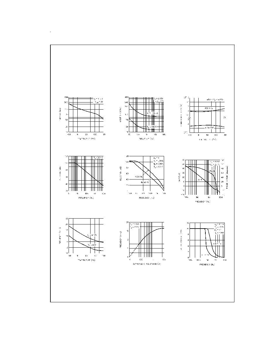
Typical Performance Characteristics
Input Bias Current
DS010254-25
Input Noise Voltage
DS010254-26
Common Mode Limits
DS010254-27
Common Mode Rejection
DS010254-28
Power Supply Rejection
DS010254-29
Frequency Response
High Frequency
DS010254-30
Unity Gain Bandwidth
DS010254-31
Unity Gain Bandwidth
vs Output Load
DS010254-32
Large Signal Response
(Sine Wave)
DS010254-33
www.national.com
4

Typical Performance Characteristics
(Continued)
Total Harmonic Distortion
DS010254-34
Output Impedance
DS010254-35
Output Saturation
DS010254-36
Output Current Limit
DS010254-37
Supply Current
(Both Amplifiers)
DS010254-38
Slew Rate
DS010254-39
Inverter Settling Time
DS010254-40
Follower Settling Time
DS010254-41
Typical Stability Range
DS010254-42
www.national.com
5