 | ÐлекÑÑоннÑй компоненÑ: LM6311 | СкаÑаÑÑ:  PDF PDF  ZIP ZIP |
LM6311 Low Noise High Speed Voltage Feedback Operational Amplifier
TL H 12546
LM6311
Low
Noise
High
Speed
Voltage
Feedback
Operational
Amplifier
November 1995
LM6311
Low Noise High Speed Voltage
Feedback Operational Amplifier
General Description
The LM6311 is a low noise voltage feedback operational
amplifier with low distortion This makes the LM6311 ideal
for signal recovery high quality video audio and medical
imaging
The conventional voltage fedback design makes it easy to
use in standard active filter circuits
The low distortion makes the LM6311 a good choice for
driving high resolution analog-to-digital converters
The 50 mA current drive and good capacitive load tolerance
make the LM6311 useful for driving analog-to-digital con-
verters which have switched-capacitor type inputs
The LM6311 provides low noise and high speed for
a
5V
single supply designs making it useful for desktop systems
and portable designs
Features
Y
110 MHz
b
3 dB bandwidth
Y
2 3 nV root-Hertz voltage noise
Y
3 5 pA root-Hertz current noise
Y
50 mA output current
Y
200V ms slew rate
Y
Low distortion
b
60 dB
5 MHz
Y
Pin for external compensation
Y
Dual
g
5V or single
a
5V or
a
12V supplies
Y
Guaranteed specs at
a
5V
Applications
Y
High end consumer audio
Y
Professional video
Y
Medical imaging
Y
Instrumentation
Y
Differential amplifiers and active filters
Y
Telecommunications signal recovery
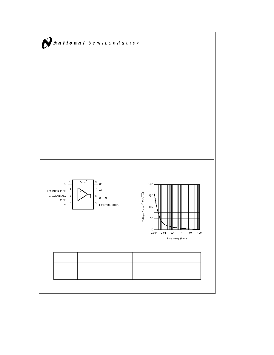
Connection Diagrams
8-Pin DIP SO-8
TL H 12546 1
Top View
LM6311 Input Referred
Voltage Noise V
a
e a
5V
TL H 12546 16
Package
Ordering
NSC Drawing
Package
Transport Media
Information
Number
Marking
8-Pin DIP
LM6311IN
N08E
LM6311IN
Rails
8-Pin SO-8
LM6311IM
M08A
LM6311IM
Rails
8-Pin SO-8
LM6311IMX
M08A
LM6311IM
2 5k Units Tape and Reel
TinyPaK
TM
is a trademark of National Semiconductor Corporation
C1996 National Semiconductor Corporation
RRD-B30M76 Printed in U S A
http
www national com
Absolute Maximum Ratings
(Note 1)
If Military Aerospace specified devices are required
please contact the National Semiconductor Sales
Office Distributors for availability and specifications
ESD Tolerance (Note 2)
2000V
Differential Input Voltage
g
10V
Voltage at Input Output Pin
(V
a
) (V
b
)
Supply Voltage (V
a
V
b
)
12V
Current at Input Pin
g
5 mA
Current at Output Pin (Note 3)
g
80 mA
Current at Power Supply Pin
80 mA
Lead Temperature (soldering 10 sec)
260 C
Storage Temp Range
b
65 C to
a
150 C
Junction Temperature (Note 4)
150 C
Operating Ratings
(Note 1)
Supply Voltage
g
2 25V to
g
6V
Junction Temperature Range
LM6311I
b
40 C
s
T
J
s
a
85 C
Thermal resistance (i
JA
)
N Package 8-pin Molded DIP
125 C W
SO-8 Package 8 Pin Surface Mount
165 C W
g
5V DC Electrical Characteristics
Unless otherwise specified all limits guaranteed for T
J
e
25 C V
a
e
5V V
b
e b
5V V
CM
e
V
O
e
0V and R
L
e
%
Boldface limits apply at the temperature extreme S
Typ
LM6311I
Symbol
Parameter
Conditions
(Note 5)
Limit
Units
(Note 6)
V
OS
Input Offset Voltage
0 5
2 5
mV
4 0
max
TCV
OS
Input Offset Voltage
5
m
V C
Average Drift
I
B
Input Bias Current
8
30
m
A
75
max
TCI
B
Input Bias Current
0 3
m
A C
Average Drift
I
offset
Input Offset Current
0 5
5
m
A
14
max
TCI
offset
Input Offset Current
0 02
m
A C
Average Drift
CMRR
Common Mode
V
CM
e
g
2 5V
90
60
db
Rejection Ratio
54
min
CMVR
Common Mode
CMRR
e
60 db
g
3 5
g
3 2
V
Voltage Range
a
PSRR
Positive Power
V
a
e
4 5V to 5V
62
db
Supply Rejection
V
b
e b
5 0V
75
55
min
Ratio
b
PSRR
Negative Power
V
a
e
5 0V
62
db
Supply Rejection
V
b
e b
4 5V to
b
5 0V
75
55
min
Ratio
C
IN-CM
Common-Mode
2 5
pF
Input Capacitance
C
IN-DIFF
Differential-Mode
2 5
pF
Input Capacitance
A
VOL
Voltage Gain
V
O
e b
2V to
a
2V
70
62
db
R
L
e
1 kX
55
http
www national com
2
g
5V DC Electrical Characteristics
Unless otherwise specified all limits guaranteed for T
J
e
25 C V
a
e
5V V
b
e b
5V V
CM
e
V
O
e
0V and R
L
e
%
Boldface limits apply at the temperature extremes (Continued)
Typ
LM6311I
Symbol
Parameter
Conditions
(Note 5)
Limit
Units
(Note 6)
V
O
Output Swing
R
L
e
100X
3 4
3 1
V
1 2
min
b
3 4
b
3 1
V
b
1 2
max
R
L
e
1 kX
3 9
3 5
V
b
2 5
min
b
3 9
b
3 5
V
b
2 5
max
R
OUT
Output Resistance
Closed Loop
0 1
X
max
I
S
Supply Current
14
16
mA
17
max
g
5V AC Electrical Characteristics
Unless otherwise specified all limits guaranteed for T
J
e
25 C V
a
e
5V V
b
e b
5V V
CM
e
V
O
e
0V and R
L
e
100X Boldface limits apply at the temperature extremes
Typ
LM6311I
Symbol
Parameter
Conditions
(Note 5)
Limit
Units
(Note 6)
SR
Slew Rate
A
V
e a
2 2V Output Pulse
200
V ms
b
3 dB BW
b
3db Bandwidth
A
V
e a
1
110
MHz
b
3 db BW
b
3 dB Bandwidth
A
V
e a
2
40
MHz
Dg
Differential Gain
A
V
e a
2 150X Load
0 12
%
(Note 7)
Dp
Differential Phase
A
V
e a
2 150X Load
0 35
Deg
(Note 7)
e
n
Input-Referred
1 MHz
k
f
k
100 MHz
2 3
nV
0
Hz
Voltage Noise
i
n
Input-Referred
1 MHz
k
f
k
100 MHz
3 5
nV
0
Hz
Current Noise
http
www national com
3
5V DC Electrical Characteristics
Unless otherwise specified all limits guaranteed for T
J
e
25 C V
a
e
5V V
b
e
0V V
CM
e
2 5V V
O
e
2 5V and R
L
e
%
Boldface limits apply at the temperature extremes
Typ
LM6311I
Symbol
Parameter
Conditions
(Note 5)
Limit
Units
(Note 6)
V
OS
Input Offset Voltage
0 3
3 0
mV
5 0
max
TCV
OS
Input Offset Voltage
5
m
V C
Average Drift
I
B
Input Bias Current
6
16
m
A
30
max
TCI
B
Input Bias Current
0 3
m
A C
Average Drift
I
offset
Input Offset Current
0 6
6
m
A
max
TCI
offset
Input Offset Current
0 02
m
A C
Average Drift
CMRR
Common Mode
V
CM
e
1 75 to 3 25
90
65
db
Rejection Ratio
50
min
a
PSRR
Positive Power Supply
V
a
e
4 75V to 6V
70
60
db
Rejection Ratio
50
min
C
IN-CM
Common-Mode
2 5
pF
Input Capacitance
C
IN-DIFF
Differential-Mode
2 5
pF
Input Capacitance
V
O
Output Swing
R
L
e
100X to 2 5V
4 2
3 6
V
3 4
min
0 9
1 4
V
1 6
max
R
L
e
1 kX to 2 5V
4 3
3 8
V
3 6
min
0 70
1 2
V
1 4
max
A
VOL
Voltage Gain
V
O
e
2 0V to 3 0V
67
55
db
R
L
e
1 kX to 2 5V
50
I
S
Supply Current
11
13
mA
14
max
http
www national com
4

5V AC Electrical Characteristics
Unless otherwise specified all limits guaranteed for T
J
e
25 C V
a
e
5V V
b
e
0V V
CM
e
2 5V V
O
e
2 5V and R
L
e
100X to 2 5V Boldface limits apply at the temperature extremes
Typ
LM6311I
Symbol
Parameter
Conditions
(Note 5)
Limit
Units
(Note 6)
SR
Slew Rate
A
V
e a
2 0 5V Output Pulse
100
V ms
b
3dB BW
b
3dB Bandwidth
A
V
e a
2
40
MHz
Note 1
Absolute maximum Ratings indicate limits beyond which damage to the device my occur Operating Ratings indicate conditions for which the device is
intended to be functional but specific performance is not guaranteed For guaranteed specifications and the test conditions see the Electrical characteristics
Note 2
Human body model 1 5 kX in series with 100 pF
Note 3
Applies to both single-supply and split-supply operation Continuous short circuit operation at elevated ambient temperature can result in exceeding the
maximum allowed junction temperature of 150 C
Note 4
The maximum power dissipation is a function of T
J(max)
i
JA
and T
A
The maximum allowable power dissipation at any ambient temperature is
P
D
e
(T
J(max)
T
A
) i
JA
All numbers apply for packages soldered directly into a PC board
Note 5
Typical values represent the most likely parametric norm
Note 6
All limits are guaranteed by testing or statistical analysis
Note 7
Differential Gain and Phase performace are sensitive to layout Follow layout suggestions in text for best results
http
www national com
5