 | –≠–ª–µ–∫—Ç—Ä–æ–Ω–Ω—ã–π –∫–æ–º–ø–æ–Ω–µ–Ω—Ç: LM6313N | –°–∫–∞—á–∞—Ç—å:  PDF PDF  ZIP ZIP |
TL H 10521
LM6313
High
Speed
High
Power
Operational
Amplifier
February 1995
LM6313 High Speed
High Power Operational Amplifier
General Description
The LM6313 is a high-speed high-power operational ampli-
fier This operational amplifier features a 35 MHz small sig-
nal bandwidth and 250 V ms slew rate A compensation pin
is included for adjusting the open loop bandwidth The input
stage (A1) and output stage (A2) are pinned out separately
and can be used independently The operational amplifier is
designed for low impedance loads and will deliver
g
300 mA The LM6313 has both overcurrent and thermal
shutdown protection with an error flag to signal both these
fault conditions
These amplifiers are built with National's VIP
TM
(Vertically
Integrated PNP) process which provides fast PNP transis-
tors that are true complements to the already fast NPN de-
vices This advanced junction-isolated process delivers high
speed performance without the need for complex and ex-
pensive dielectric isolation
Features
Y
High slew rate
250 V ms
Y
Wide bandwidth
35 MHz
Y
Peak output current
g
300 mA
Y
Input and output stages pinned out separately
Y
Single or dual supply operation
Y
Thermal protection
Y
Error flag warns of faults
Y
Wide supply voltage range
g
5V to
g
15V
Applications
Y
High speed ATE pin driver
Y
Data acquisition
Y
Driving capacitive loads
Y
Flash A-D input driver
Y
Precision 50X ≠ 75X video line driver
Y
Laser diode driver
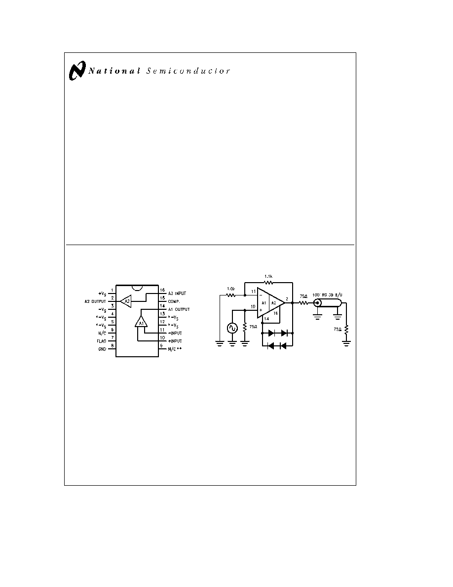
Connection Diagram
Dual-In-Line Package
TL H 10521 ≠ 1
Top View
Order Number LM6313N
See NS Package Number N16A
Heat sink pins
See Note 5 and Applications
Do not ground or otherwise connect to this pin
Typical Application
TL H 10521 ≠ 2
VIP
TM
is a trademark of National Semiconductor Corporation
C1995 National Semiconductor Corporation
RRD-B30M75 Printed in U S A
Absolute Maximum Ratings
(Note 1)
Total Supply Voltage (
a
V
S
to
b
V
S
)
36V (
g
18)
A1 Differential Input Voltage (Note 2)
g
7V
A1 Input Voltage
(V
a
b
0 7) to (V
b
b
7V)
A2 Input to Output Voltage
g
7V
A2 Input Voltage
g
V
S
Flag Output Voltage
GND to
a
V
S
Short-Circuit to Ground
(Note 3)
Storage Temperature Range
b
65 C
s
T
s
a
150 C
Lead Temperature (Soldering 5 seconds)
260 C
ESD Tolerance (Note 4)
Pins 10 and 11
g
600V
All Other Pins
g
1500V
Operating Temperature Range
LM6313N
0 C to 70 C
Thermal Derating Information (Note 5)
i
JA
40 C W
T
J
(Max)
125 C
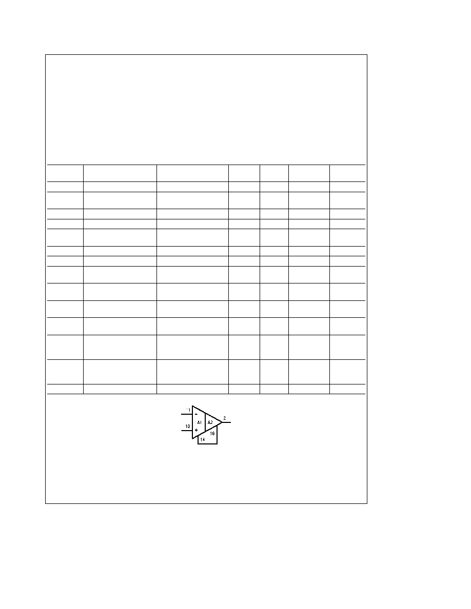
Operational Amplifier DC Electrical Characteristics
Unless otherwise specified all limits
guaranteed for T
A
e
25 C and Supply Voltage V
S
e
g
15V Boldface limits apply at temperature extremes V
CM
e
0V
R
S
e
50X the circuit configured as in
Figure 1
Symbol
Parameter
Conditions
Typical
25 C
0 C to 70 C
Units
Limit
Limit
V
OS
Input Offset Voltage
5
20
22
mV (Max)
D
V
OS
D
T
Average Input Offset
10
m
V C
Voltage Drift
I
b
Input Bias Current
2
5
7
m
A (Max)
I
OS
Input Offset Current
0 15
1 5
1 9
m
A (Max)
D
I
OS
D
T
Average Input Offset
0 4
nA C
Current Drift
R
IN
Input Resistance
Differential
325
kX
C
IN
Input Capacitance
A
V
e a
1 f
e
10 MHz
2 2
pF
V
CM
Common-Mode
a
14 2
a
13 8
a
13 7
V (Min)
Voltage Range
b
13 2
b
12 8
b
12 7
A
V1
Voltage Gain 1
R
L
e
1 kX V
O
e
g
10V
6000
2500
2000
V V (Min)
A
V2
Voltage Gain 2
R
L
e
50X V
O
e
g
8V
5000
2000
1500
CMRR
Common-Mode
b
10V
s
V
CM
s
a
10V
90
72
70
dB (Min)
Rejection Ratio
PSRR
Power Supply
g
5V
s
V
S
s g
16V
90
72
70
dB (Min)
Rejection Ratio
V
O1
Output Voltage Swing 1
R
L
e
1 kX
13 1
11 8
11 2
V
O2
Output Voltage Swing 2
R
L
e
100X
12 0
10 5
10 0
g
V (Min)
V
O3
Output Voltage Swing 3
R
L
e
50X
11 0
9 0
8 5
I
S
Supply Current
T
J
e
0 C
24
T
J
e
25 C
18
23
mA (Max)
T
J
e
125 C
21
I
SC
Peak Short-Circuit Output
(See
Figure 3 )
300
mA
TL H 10521 ≠ 3
FIGURE 1
2
Electrical Characteristics
(Continued)
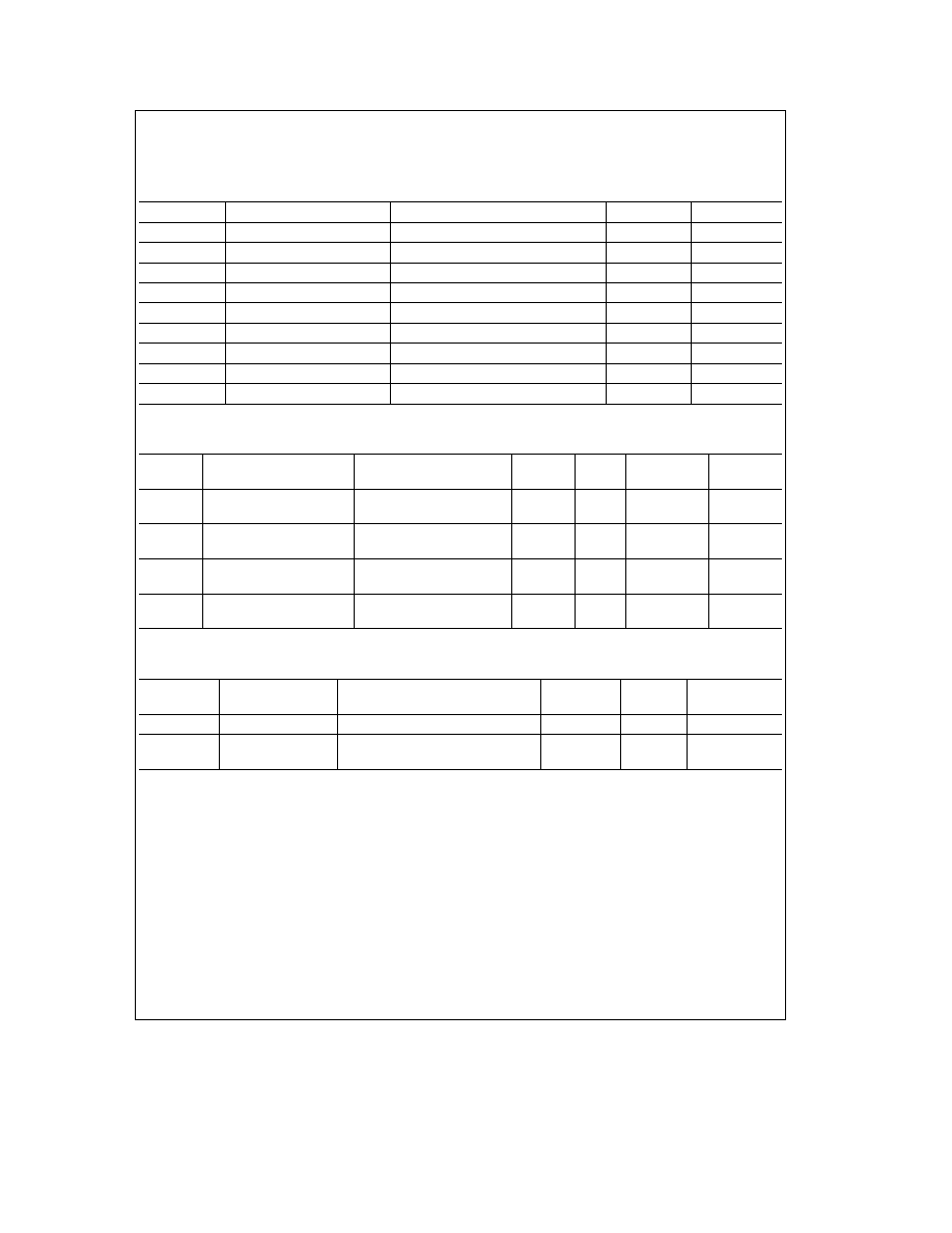
Operational Amplifier AC Electrical Characteristics
Unless otherwise specified all limits
guaranteed for T
A
e
25 C and Supply Voltage V
S
e
g
15V Boldface limits apply at temperature extremes V
CM
e
0V
R
S
e
50X the circuit configured as in
Figure 1
Symbol
Parameter
Conditions
Typical
Units
GBW
Gain-Bandwidth Product
f
e
30 MHz
35
MHz
SR
Slew Rate
A
V
e b
1 R
L
e
50X (Note 6)
250
V ms
PBW
Power Bandwidth
V
OUT
e
20 V
PP
3 0
MHz
t
S
Settling Time
10V Step to 0 1% (See
Figure 2 )
200
ns
Phase Margin
A
V
e b
1 R
L
e
1 kX C
L
e
50 pF
53
Deg
Differential Gain
0 1
%
Differential Phase
0 1
Deg
e
n
Input Noise Voltage
f
e
10 kHz
14
nV
S
Hz
i
n
Input Noise Current
f
e
10 kHz
1 8
pA
S
Hz
A1 DC Electrical Characteristics
Unless otherwise specified all limits guaranteed for T
A
e
25 C and
Supply Voltage V
S
e
g
15V Boldface limits apply at temperature extremes V
CM
e
0V R
S
e
50X
Symbol
Parameter
Conditions
Typical
25 C
0 C to 70 C
Units
Limit
Limit
A
VOL
Large Signal Voltage Gain
V
OUT
e
g
10V R
L
e
2 kX
650
300
250
V V (Min)
V
OUT
e
g
10V R
L
e
%
6000
2500
2000
CMRR
Common-Mode
b
10V
s
V
CM
s
a
10V
90
72
70
dB (Min)
Rejection Ratio
PSRR
Power Supply
g
5V
s g
V
S
s
a
16V
90
72
70
dB (Min)
Rejection Ratio
I
SC
Output Short
g
60
g
30
g
25
mA (Min)
Circuit Current
A1 AC Electrical Characteristics
Unless otherwise specified all limits guaranteed for T
A
e
25 C and
Supply Voltage V
S
e
g
15V Boldface limits apply at temperature extremes R
S
e
50X
Symbol
Parameter
Conditions
Typical
25 C
Units
Limit
GBW
Gain-Bandwidth
f
e
30 MHz
37
25
MHz (Min)
SR
Slew Rate
A
V
e a
1 R
L
e
100 kX
g
4 V
IN
250
150
V ms (Min)
g
2 V
OUT
Note 1
Absolute Maximum Ratings indicate limits beyond which damage to the device may occur For guaranteed specifications and test conditions see the
Electrical Characteristics The guaranteed specifications apply only for the test condition listed Some performance characteristics may degrade when the device is
not operated under the listed test conditions
Note 2
In order to achieve optimum AC performance the input stage was designed without protective clamps Exceeding the maximum differential input voltage
results in reverse breakdown of the base-emitter junction of one of the input transistors Degradation of the input parameters (especially V
OS
I
OS
and Noise) is
proportional to the level of the externally limited breakdown current and the accumulated duration of the breakdown condition
Note 3
Continuous short-circuit operation of A1 at elevated temperature can result in exceeding the maximum allowed junction temperature of 125 C A2 contains
current limit and thermal shutdown to protect against fault conditions The device may be damaged by shorts to the supplies
Note 4
Human body model C
e
100 pF R
S
e
1500X
3
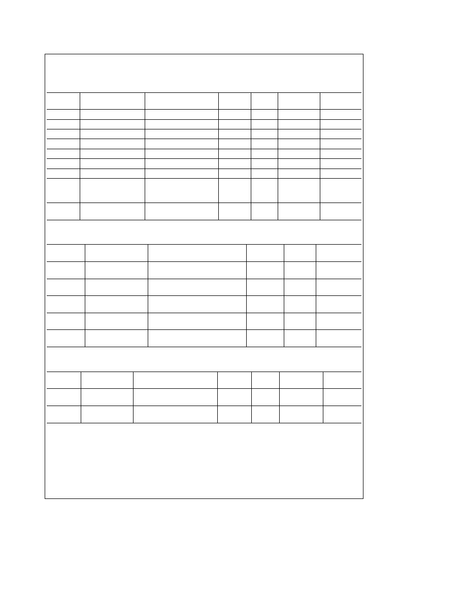
Electrical Characteristics
(Continued)
A2 DC Electrical Characteristics
Unless otherwise specified all limits guaranteed for T
A
e
25 C and
Supply Voltage V
S
e
g
15V Boldface limits apply at temperature extremes R
S
e
50X
Symbol
Parameter
Conditions
Typical
25 C
0 C to 70 C
Units
Limit
Limit
A
V1
Voltage Gain 1
R
L
e
1 kX V
IN
e
g
10V
0 99
0 97
0 95
V mV (Min)
A
V2
Voltage Gain 2
R
L
e
50X V
IN
e
g
10V
0 9
0 85
0 82
V V (Min)
V
OS
Offset Voltage
R
L
e
1 kX
15
70
100
mV (Max)
I
b
Input Bias Current
R
L
e
1 kX R
S
e
10 kX
1
6
8
m
A (Max)
R
IN
Input Resistance
R
L
e
50X
5
MX
C
IN
Input Capacitance
3 5
pF
R
O
Output Resistance
I
OUT
e
g
10 mA
3 5
5 0
8 0
X
(Min)
V
O
Voltage Output Swing
R
L
e
1 kX
13 7
13 0
12 7
R
L
e
100X
12 5
10 5
10 0
V (Min)
R
L
e
50X
11 0
9 0
8 5
PSRR
Power Supply
V
S
e
g
5V to
g
16V
70
60
50
dB (Min)
Rejection Ratio
A2 AC Electrical Characteristics
Unless otherwise specified all limits guaranteed for T
A
e
25 C and
Supply Voltage V
S
e
g
15V Boldface limits apply at temperature extremes R
S
e
50X
Symbol
Parameter
Conditions
Typical
25 C
Units
Limit
SR 1
Slew Rate 1
V
IN
e
g
11V R
L
e
1 kX
1200
V ms (Min)
SR 2
Slew Rate 2
V
IN
e
g
11V R
L
e
50X (Note 7)
750
550
BW
b
3 dB Bandwidth
V
IN
e
g
100 mVpp
65
30
MHz (Min)
R
L
e
50X C
L
s
10 pF
t
r
Rise Time
R
L
e
1 kX C
L
s
10 pF
8
ns
t
f
Fall Time
V
O
e
100 mVpp
P
D
Propagation Delay
R
L
e
50X C
L
s
10 pF
4
ns
V
O
e
100 mVpp
Overshoot
R
L
e
1 kX C
L
e
100 pF
13
%
R
L
e
50X C
L
e
1000 pF
21
Additional (A2) Electrical Characteristics
Unless otherwise specified all limits guaranteed for
T
A
e
25 C and Supply Voltage V
S
e
g
15V Boldface limits apply at temperature extremes
Symbol
Parameter
Conditions
Typical
25 C
0 C to 70 C
Units
Limit
Limit
V
OL
Flag Pin Output
I
SINK
Flag Pin
e
500 mA
220
340
400
mV (Max)
Low Voltage
I
OH
Flag Pin Output
V
OH
Flag Pin
e
15V (Note 8)
0 01
10
20
m
A (Max)
High Current
Note 5
For operation at elevated temperature these devices must be derated to insure T
J
s
125 C T
J
e
T
A
a
(P
D
c
i
JA
) i
JA
for the N package mounted flush
to the PCB is 40 C W when pins 4 5 12 and 13 are soldered to a total of 2 in
2
of copper trace
Note 6
Measured between
g
5V
Note 7
V
IN
e g
9V step input measured between
g
5V out
Note 8
The error flag is set during current limit or thermal shut-down The flag is an open collector low on fault
4
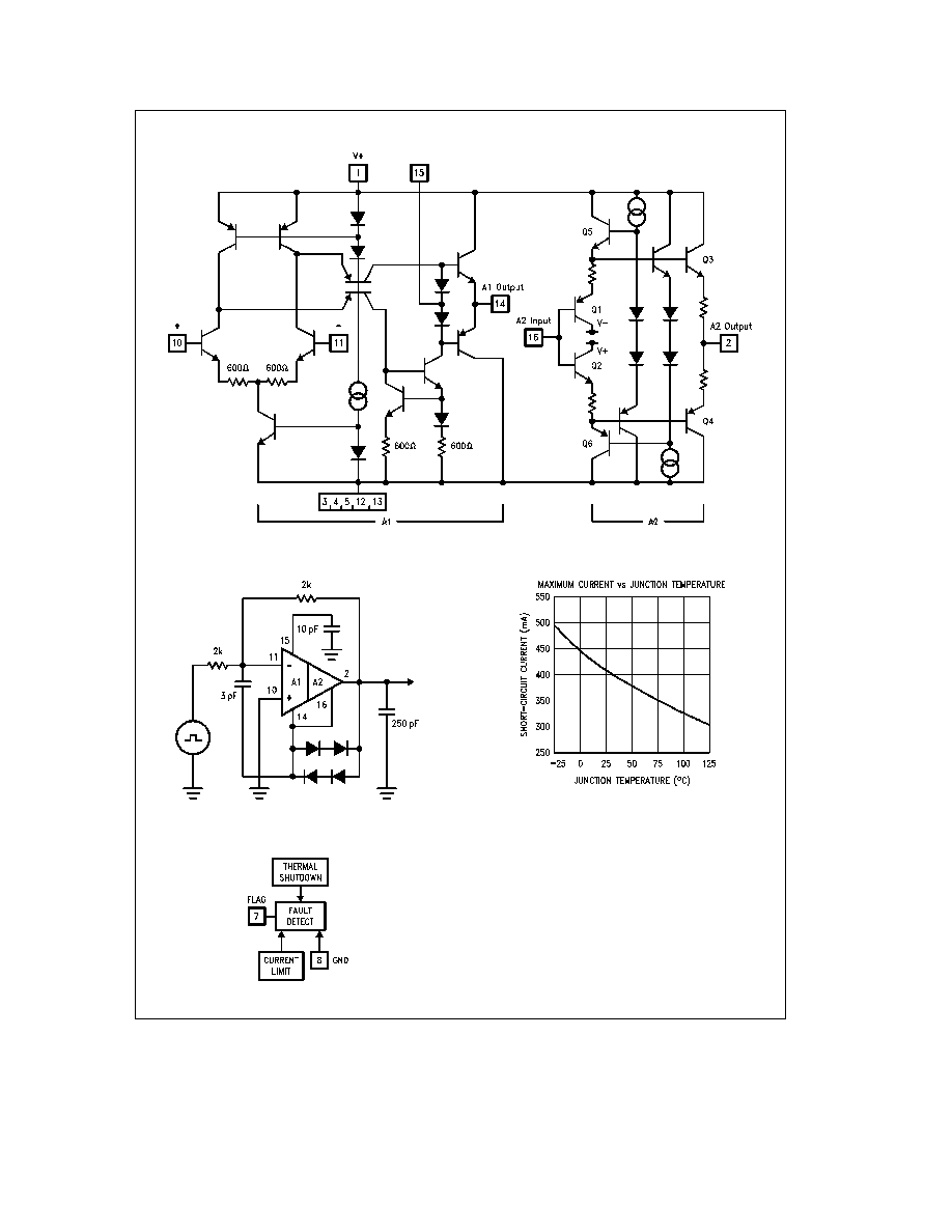
Simplified Schematic
TL H 10521 ≠ 4
Settling Time Test Circuit
TL H 10521 ≠ 5
FIGURE 2
TL H 10521 ≠ 6
FIGURE 3
Protection Circuit Block Diagram
TL H 10521 ≠ 7
5