 | ÐлекÑÑоннÑй компоненÑ: LM6317 | СкаÑаÑÑ:  PDF PDF  ZIP ZIP |
Äîêóìåíòàöèÿ è îïèñàíèÿ www.docs.chipfind.ru
TL H 12542
LM6317
120
MHz
Fast
Settling
Low
Power
Voltage
Feedback
Amplifier
November 1995
LM6317
120 MHz Fast Settling Low Power
Voltage Feedback Amplifier
General Description
The LM6317 is a high speed unity-gain stable voltage feed-
back amplifier that consumes only 40 mW of quiescent pow-
er Operating at
g
5V power supply the LM6317 provides
excellent AC performance such as 120 MHz of unity-gain
bandwidth 1500V ms of slew rate and 80 dB of SFDR
The LM6317 has the slew characteristic of a current feed-
back amplifier yet it can be used in all traditional amplifier
configurations The high output current and good stability
with capacitive load of LM6317 makes it ideal for driving
cables With its unity-gain stability fast settling time and low
output impedance the LM6317 can be used to buffer A D
converters The LM6317 also has very low input voltage and
current noise high CMRR and PSRR desirable in precision
applications such as ATE systems
Features
(Typical unless otherwise noted)
Y
Easy to use voltage feedback topology
Y
Unity-gain stability
Y
Wide unity-gain bandwidth
120 MHz
Y
Fast slew rate
1100V ms
Y
Fast settling time
0 1%
12 ns
0 01%
18 ns
Y
Low SFDR
1 MHz Driving 100X
80 dB
Y
High output current
60 mA
Y
High CMRR and PSRR
80 dB 74 dB
Y
Low supply current
4 mA
Y
Specified for
g
5V operation
Applications
Y
Active filters
Y
A D Converter buffers
Y
Video cable drivers
Y
Communication systems
Y
Portable systems
Y
Ultrasound equipment
Y
ATE systems
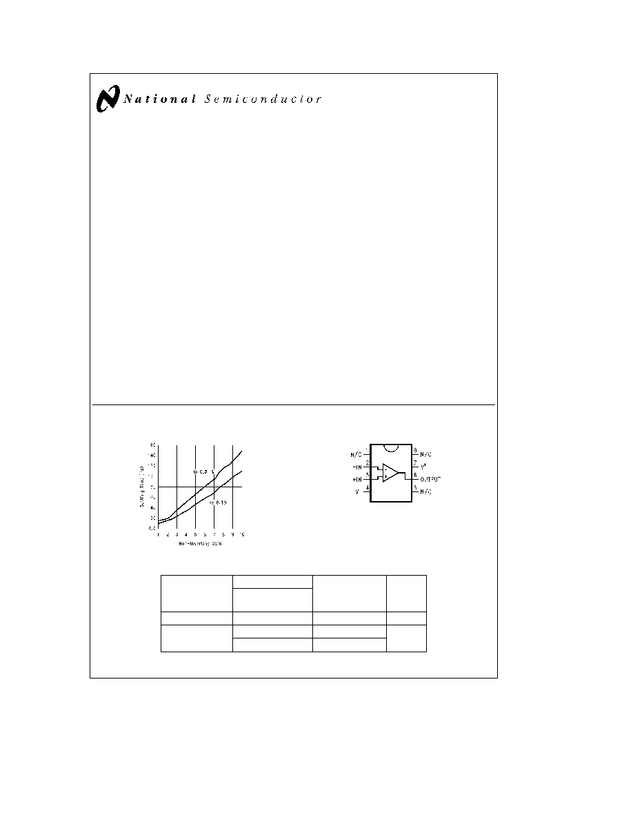
Typical Performance
Settling Time vs Gain
TL H 12542 14
Connection Diagram
8-Pin DIP SO
TL H 12542 2
Top View
Ordering Information
Package
Temperature Range
Transport
Media
Drawing
NSC
Industrial
b
40 C to
a
85 C
8-Pin DIP
LM6317IN
Rails
N08E
8-Pin Small Outline
LM6317IM
Rails
M08A
LM6317IMX
2 5k Tape and Reel
TinyPak
TM
is a trademark of National Semiconductor Corp
C1996 National Semiconductor Corporation
RRD-B30M76 Printed in U S A
http
www national com
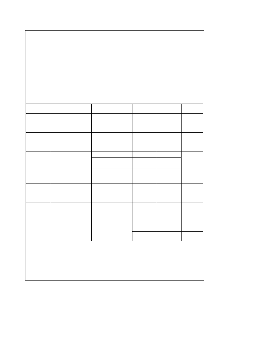
Absolute Maximum Ratings
(Note 1)
If Military Aerospace specified devices are required
please contact the National Semiconductor Sales
Office Distributors for availability and specifications
ESD Tolerance (Note 2)
Human Body Model
1 5 kV
Machine Model
200V
Supply Voltage (V
a
V
b
)
12V
Differentfial Input Voltage
10V
Output Current (Note 3)
g
60 mA
Storage Temperature Range
b
65 C to
a
150 C
Maximum Junction Temperature (Note 4)
150 C
Operating Ratings
(Note 1)
Supply Voltage
g
2 3V
s
V
S
s g
6V
Junction Temperature Range
b
40 C
s
T
J
s
a
85 C
Thermal Resistance (i
JA
)
N Package 8-Pin Molded DIP
110 C W
M Package 8-Pin Surface Mount
170 C W
g
5V DC Electrical Characteristics
Unless otherwise specified all limits guaranteed for T
J
e
25 C
V
a
e a
5V V
b
e b
5V V
CM
e
0V and R
L
e
100X Boldface limits apply at the temperature extremes
Symbol
Parameter
Conditions
Typ
Limit
Units
(Note 5)
(Note 6)
V
OS
Input Offset Voltage
0 3
5
mV
7
max
TC V
OS
Input Offset Voltage
8
m
V C
Average Drift
I
B
Input Bias Current
3
12
m
A
22
max
I
OS
Input Offset Current
0 2
2
m
A
4
max
R
IN
Input Resistance
Differential
2
MX
Common
1
C
IN
Input Capacitance
Differential
1
pF
Common
1
R
O
Open Loop Output
0 02
X
Resistance
CMRR
Common Mode
V
CM
e
g
1 5V
80
62
dB
Rejection Ratio
57
min
PSRR
Power Supply
V
S
e
g
5V to
g
4 5V
74
60
dB
Rejection Ratio
52
min
A
V
Large Signal
V
OUT
e
g
1V
70
55
min
dB
Voltage Gain
R
L
e
1 kX
50
V
OUT
e
g
1V
67
53
R
L
e
100X
48
V
CM
Input Common-Mode
CMRR
e
60 dB
3 2
2 6
V
Voltage Range
2 3
min
b
3 2
b
2 6
V
b
2 3
max
http
www national com
2
g
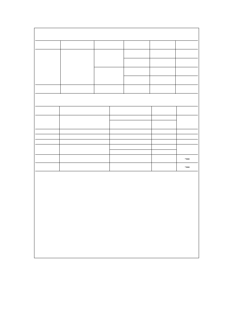
5V DC Electrical Characteristics
(Continued) Unless otherwise specified all limits guaranteed for T
J
e
25 C V
a
e a
5V V
b
e b
5V V
CM
e
0V and R
L
e
100X Boldface limits apply at the temperature extremes
Symbol
Parameter
Conditions
Typ
Limit
Units
(Note 5)
(Note 6)
V
O
Output Swing
R
L
e
1 kX
3 5
3
V
2 6
min
b
3 5
b
3
V
b
2 6
max
R
L
e
100X
3
2 5
V
2 3
min
b
3
b
2 5
V
b
2 3
max
I
S
Supply Current
4
6
mA
7
max
g
5V AC Electrical Characteristics
Unless otherwise specified T
J
e
25 C V
a
e a
5V V
b
e
5V A
V
e
1 and R
L
e
100X
Symbol
Parameter
Conditions
Typ
Units
(Note 5)
SR
Slew Rate
5V Step
1100
V ms
5V Step A
V
e b
1
750
R
L
e
500X
Unity-Gain Bandwidth
A
V
e b
1 R
L
e
500X
120
MHz
b
3 dB Frequency
A
V
e a
2
80
MHz
i
m
Phase Margin
A
V
e b
1 R
L
e
500X
60
t
s
Settling Time
0 1% 2V Step
12
ns
0 01% 2V Step
18
e
n
Input-Referred Voltage Noise
f
e
100 kHz
4 2
nV
0
Hz
i
n
Input-Referred Current Noise
f
e
100 kHz
2
pA
0
Hz
Note 1
Absolute Maximum Ratings indicate limits beyond which damage to the device may occur Operating Ratings indicate conditions for which the device is
intended to be functional but specific performance is not guaranteed For guaranteed specifications and the test conditions see the Electrical Characteristics
Note 2
Human body model 1 5 kX in series with 100 pF Machine model 200X in series with 100 pF
Note 3
Applies to both single-supply and split-supply operation Sourcing and sinking more than 60 mA at the output may adversely affect reliability
Note 4
The maximum power dissipation is a function of T
J(max)
i
JA
and T
A
The maximum allowable power dissipation at any ambient temperature is P
D
e
(T
J(max)
T
A
) i
JA
All numbers apply for packages soldered directly into a PC board
Note 5
Typical values represent the most likely parametric norm
Note 6
All limits are guaranteed by testing or statistical analysis
http
www national com
3
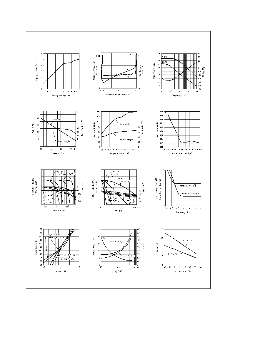
Typical Performance Characteristics
Unless otherwise noted T
A
e
25 C V
S
e
g
5V
vs Supply Voltage
Supply Current
TL H 12542 3
Common-Mode Voltage
I
B
and I
OS
vs
TL H 12542 4
Closed Loop R
o
PSRR CMRR and
TL H 12542 5
Frequency Response
Open Loop
vs Supply Voltage
Bandwidth
TL H 12542 7
vs Capacitive Load
Bandwidth
TL H 12542 8
Frequency Response
Non-Inverting
TL H 12542 9
Response
Inverting Frequency
TL H 12542 10
Equivalent Input Noise
TL H 12542 11
Harmonic Distortion
2nd and 3rd
TL H 12542 12
Capactive Load
Settling Time vs
TL H 12542 13
vs Ambient Temperature
Maximum Power Dissipation
TL H 12542 24
http
www national com
4
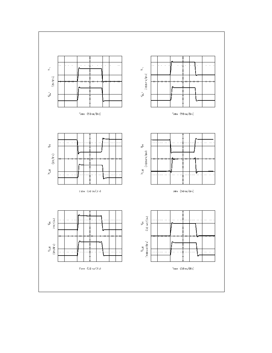
Typical Performance Characteristics
Unless otherwise noted T
A
e
25 C V
S
e
g
5V (Continued)
(A
V
e a
1)
Large Signal Pulse Response
TL H 12542 1
(A
V
e a
1)
Small Signal Pulse Response
TL H 12542 15
(A
V
e b
1)
Large Signal Pulse Response
TL H 12542 16
(A
V
e b
1)
Small Signal Pulse Response
TL H 12542 17
(A
V
e a
2)
Large Signal Pulse Response
TL H 12542 18
(A
V
e a
2)
Small Signal Pulse Response
TL H 12542 19
http
www national com
5