 | –≠–Ľ–Ķ–ļ—ā—Ä–ĺ–Ĺ–Ĺ—č–Ļ –ļ–ĺ–ľ–Ņ–ĺ–Ĺ–Ķ–Ĺ—ā: LM63DIMAX | –°–ļ–į—á–į—ā—Ć:  PDF PDF  ZIP ZIP |
LM63
Ī
1įC/
Ī
3įC Accurate Remote Diode Digital Temperature
Sensor with Integrated Fan Control
General Description
The LM63 is a remote diode temperature sensor with inte-
grated fan control. The LM63 accurately measures: (1) its
own temperature and (2) the temperature of a diode-
connected transistor, such as a 2N3904, or a thermal diode
commonly found on Computer Processors, Graphics Pro-
cessor Units (GPU) and other ASIC's. The LM63 remote
temperature sensor's accuracy is factory trimmed for the
series resistance and 1.0021 non-ideality of the Intel
ģ
0.13
Ķm Pentium
ģ
4 and Mobile Pentium 4 Processor-M thermal
diode. The LM63 has an offset register to correct for errors
caused by different non-ideality factors of other thermal di-
odes.
For
the
latest
information
contact
hardware.monitor.team
@
nsc.com.
The
LM63
also
features
an
integrated,
pulse-width-
modulated (PWM), open-drain fan control output. Fan speed
is a combination of the remote temperature reading, the
lookup table and the register settings. The 8-step Lookup
Table enables the user to program a non-linear fan speed vs.
temperature transfer function often used to quiet acoustic
fan noise.
Features
n
Accurately senses diode-connected 2N3904 transistors
or thermal diodes on-board large processors or ASIC's
n
Accurately senses its own temperature
n
Factory trimmed for Intel Pentium 4 and Mobile Pentium
4 Processor-M thermal diodes
n
Integrated PWM fan speed control output
n
Acoustic fan noise reduction with User-programmable
8-step Lookup Table
n
Multi-function, user-selectable pin for either ALERT
output, or Tachometer input, functions
n
Tachometer input for measuring fan RPM
n
Offset register can adjust for a variety of thermal diodes
n
10 bit plus sign remote diode temperature data format,
with 0.125įC resolution
n
SMBus 2.0 compatible interface, supports TIMEOUT
n
LM86-compatible pinout
n
LM86-compatible register set
n
8-pin SOIC package
Key Specifications
j
Remote Diode Temp Accuracy
(with quantization
error)
Ambient
Temp
Diode
Temp
I
PWML
Max
Version
Max
Error
30 to 50įC
60 to 100įC
5 mA
LM63C
Ī
1.0įC
30 to 50įC
60 to 100įC
5 mA
LM63D
Ī
3.0įC
0 to 85įC
25 to 125įC
8 mA
All
Ī
3.0įC
j
Local Temp Accuracy (includes quantization error)
Ambient Temp
Max Error
25įC to 125įC
Ī
3.0įC
j
Supply Voltage
3.0 V to 3.6 V
j
Supply Current
1.3 mA (typ)
Applications
n
Computer Processor Thermal Management
(Laptop, Desktop, Workstations, Servers)
n
Graphics Processor Thermal Management
n
Electronic Test Equipment
n
Projectors
n
Office Equipment
n
Industrial Controls
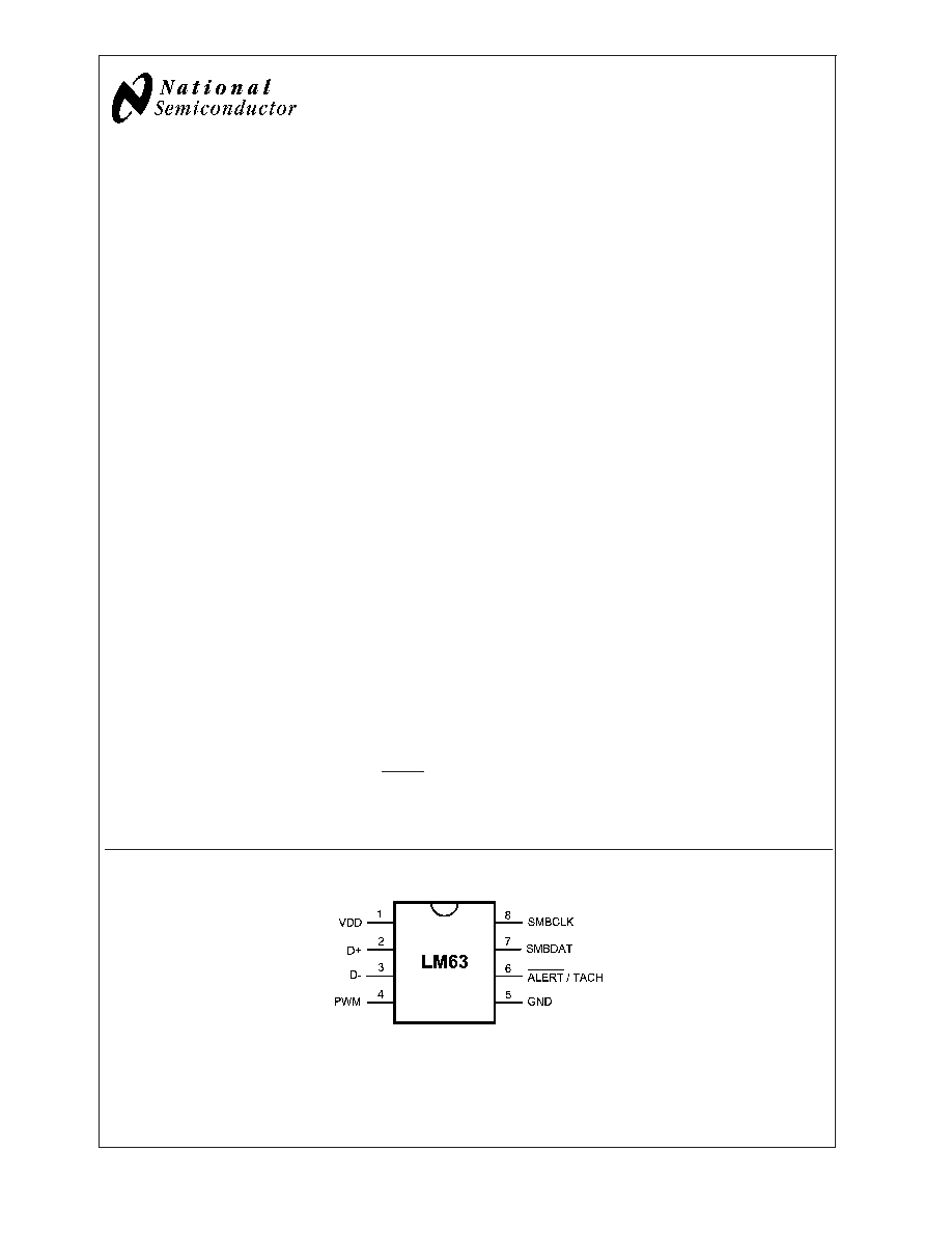
Connection Diagram
20057001
Intel
ģ
and Pentium
ģ
are registered trademarks of Intel Corporation.
May 2003
LM63
Ī
1įC/
Ī
3įC
Accurate
Remote
Diode
Digital
T
emperature
Sensor
with
Integrated
Fan
Control
© 2003 National Semiconductor Corporation
DS200570
www.national.com
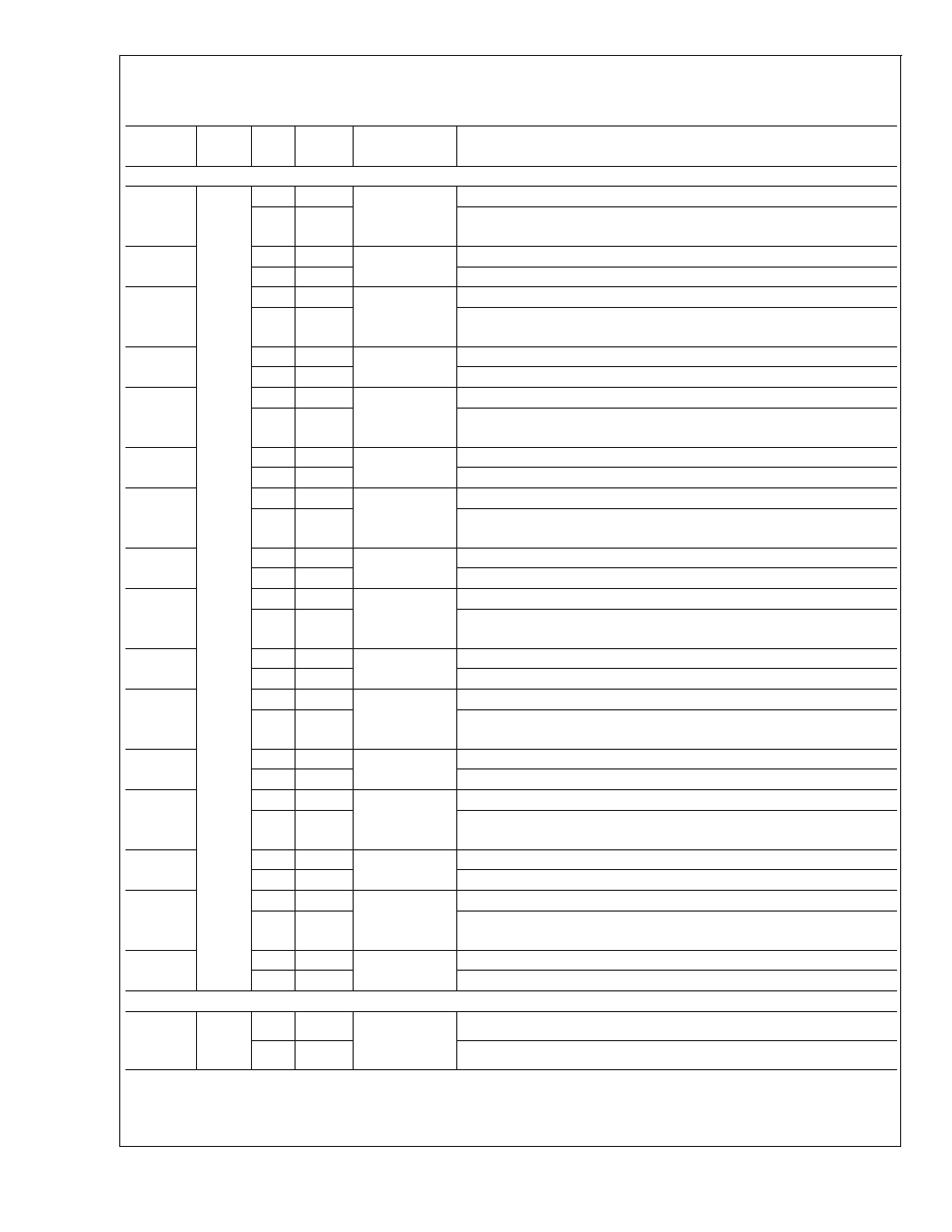
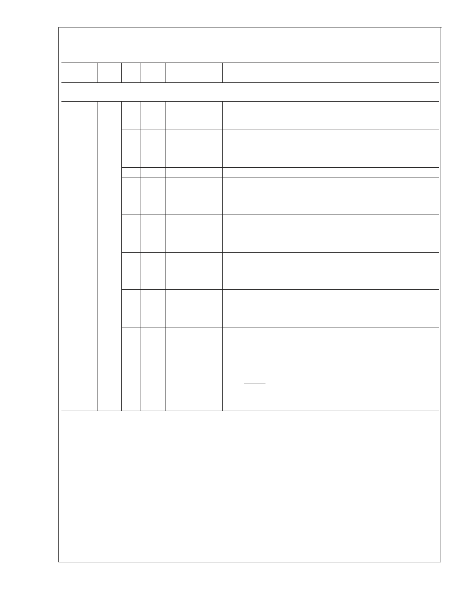
Pin Descriptions
Pin
Name
Input/Output
Function and Connection
1
V
DD
Power Supply Input
Connect to a low-noise +3.3
Ī
0.3 VDC power supply, and bypass to GND
with a 0.1 ĶF ceramic capacitor in parallel with a 100 pF ceramic capacitor.
A bulk capacitance of 10 ĶF needs to be in the vicinity of the LM63's V
DD
pin.
2
D+
Analog Input
Connect to the anode (positive side) of the remote diode. A 2.2 nF ceramic
capacitor must be connected between pins 2 and 3.
3
D-
Analog Input
Connect to the cathode (negative side) of the remote diode. A 2.2 nF
ceramic capacitor must be connected between pins 2 and 3.
4
PWM
Open-Drain
Digital Output
Open-Drain Digital Output. Connect to fan drive circuitry. The power-on
default for this pin is low (pin 4 pulled to ground).
5
GND
Ground
This is the analog and digital ground return.
6
ALERT/TACH
Digital I/O
Depending on how the LM63 is programmed, this pin is either an
open-drain ALERT output or a tachometer input for measuring fan speed.
The power-on default for this pin is the ALERT function.
7
SMBDAT
Digital Input/
Open-Drain Output
This is the bi-directional SMBus data line.
8
SMBCLK
Digital Input
Digital Input. This is the SMBus clock input.
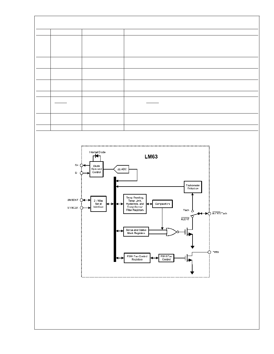
Simplified Block Diagram
20057002
LM63
www.national.com
2
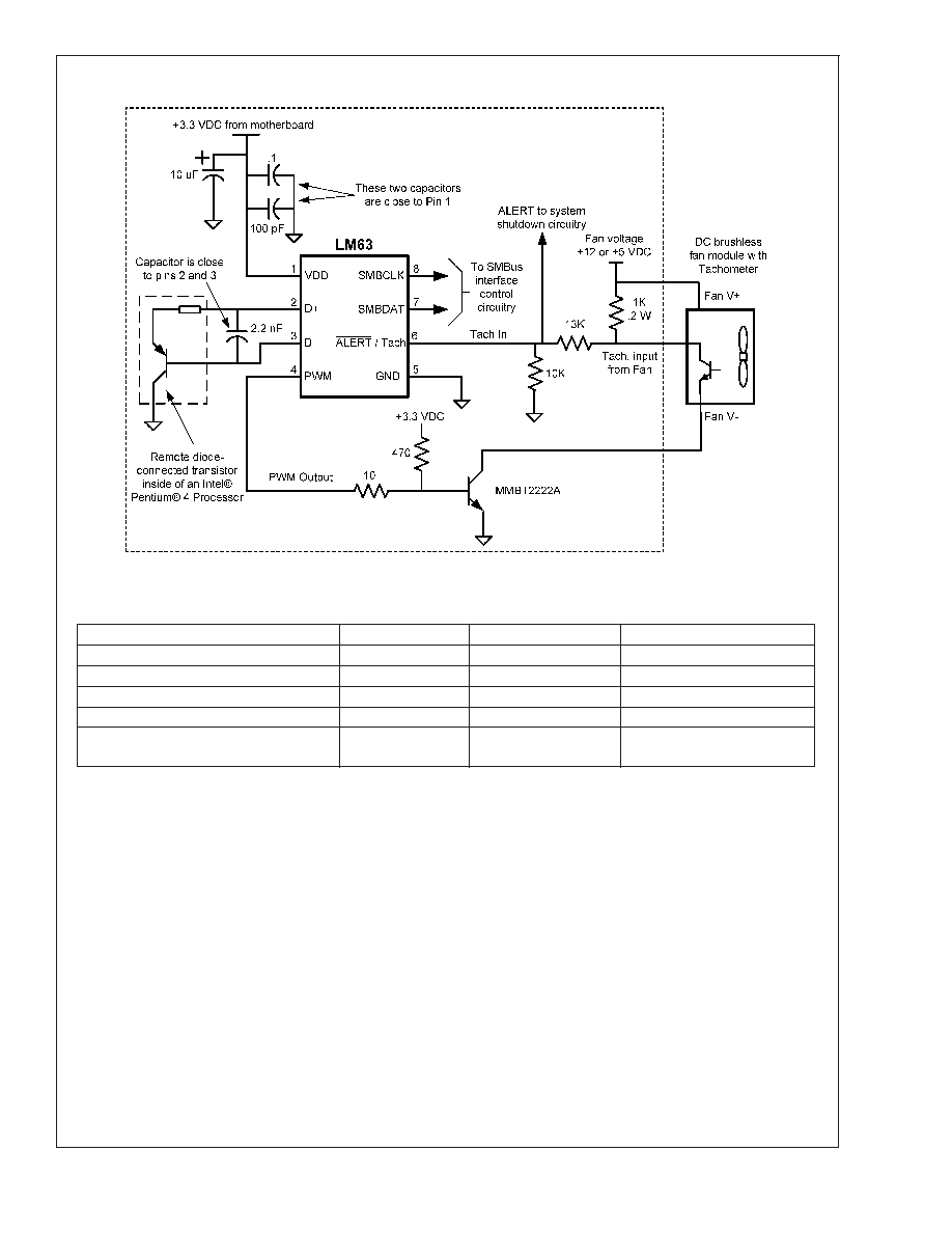
Typical Application
20057003
Ordering Information
Part Description
Top Mark
Order Number
Transport Media
LM63C (
Ī
1įC) 8-pin SOIC
LM63CIMA
LM63CIMAX
2500 Units in Tape and Reel
LM63C (
Ī
1įC) 8-pin SOIC
LM63CIMA
LM63CIMA
95 Units in Rail
LM63D (
Ī
3įC) 8-pin SOIC
LM63DIMA
LM63DIMAX
2500 Units in Tape and Reel
LM63D (
Ī
3įC) 8-pin SOIC
LM63DIMA
LM63DIMA
95 Units in Rail
LM63 Evaluation Board
With Software and User's Guide
N/A
LM63EVAL
Packaged
LM63
www.national.com
3

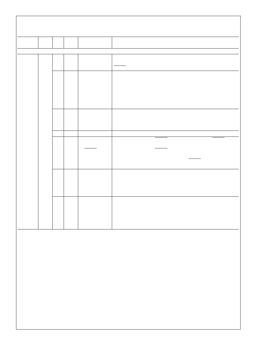
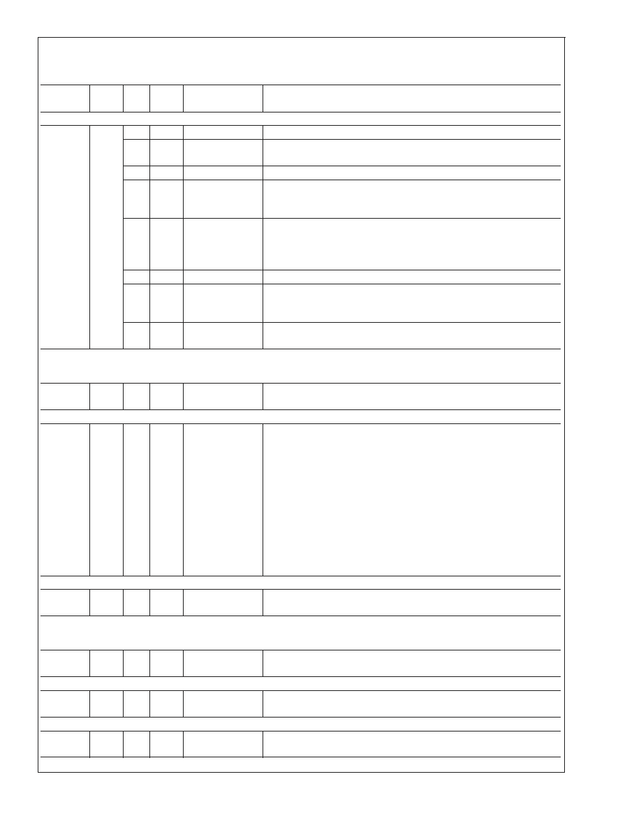
Absolute Maximum Ratings
(Notes 1,
2)
Supply Voltage, V
DD
-0.3 V to 6.0 V
Voltage on SMBDAT, SMBCLK,
ALERT/Tach, PWM Pins
-0.5 V to 6.0 V
Voltage on Other Pins
-0.3 V to (V
DD
+ 0. 3 V)
Input Current, D- Pin
Ī
1 mA
Input Current at All Other Pins (Note 3)
5 mA
Package Input Current (Note 3)
30 mA
Package Power Dissipation
(Note 5)
SMBDAT, ALERT, PWM pins
Output Sink Current
10 mA
Storage Temperature
-65įC to +150įC
ESD Susceptibility (Note 4)
Human Body Model
2000 V
Machine Model
200 V
Soldering Information, Lead Temperature
SOIC-8 Package (Note 6)
Vapor Phase (60 seconds)
215įC
Infrared (15 seconds)
220įC
Operating Ratings
(Notes 1, 2)
Specified Temperature Range
T
MIN
T
A
T
MAX
LM63CIM, LM63DIM
0įC
T
A
+85įC
Remote Diode Temperature Range
0įC
T
A
+125įC
Supply Voltage Range (V
DD
)
+3.0 V to +3.6 V
DC Electrical Characteristics
TEMPERATURE-TO-DIGITAL CONVERTER CHARACTERISTICS The following specifications apply for V
DD
= 3.0 VDC to
3.6 VDC, and all analog source impedance R
S
= 50
unless otherwise specified in the conditions. Boldface limits apply for
T
A
= T
MIN
to T
MAX
; all other limits T
A
= +25įC.
Parameter
Conditions
Version
Typical
(Note 7)
Limits
(Note 8)
Units
(Limits)
Temperature Error Using the Remote
Thermal Diode of an Intel Pentium 4
or Mobile Pentium 4 Processor-M
with typical non-ideality of 1.0021.For
other processors e-mail
hardware.monitor.team
@
nsc.com to
obtain the latest data.
T
A
= +30 to +50įC
I
PWML
5 mA
T
D
= +60 to +100įC
T
D
= Remote Diode
Junction Temperature
LM63C
Ī
1
įC (max)
LM63D
Ī
3
įC (max)
T
A
= +0 to +85įC
I
PWML
8 mA
T
D
= +25 to +125įC
All
Ī
3
įC (max)
Temperature Error Using the Local
Diode
T
A
= +25 to +125įC (Note 10)
All
Ī
1
Ī
3
įC (max)
Remote Diode Resolution
All
11
Bits
0.125
įC
Local Diode Resolution
All
8
Bits
1
įC
Conversion Time, All Temperatures
Fastest Setting
All
31.25
34.4
ms (max)
D- Source Voltage
All
0.7
V
Diode Source Current
(V
D+
- V
D-
) = +0.65 V; High Current
All
160
315
ĶA (max)
110
ĶA (min)
Low Current
All
13
20
ĶA (max)
7
ĶA (min)
Operating Electrical Characteristics
Parameter
Conditions
Typ
(Note 7)
Limits
(Note 8)
Units
ALERT and PWM Output Saturation Voltage
ALERT
PWM
I
OUT
4 mA
5 mA
0.4
V (max)
I
OUT
6 mA
0.55
Power-On-Reset Threshold Voltage
2.4
V (max)
1.8
V (min)
Supply Current (Note 9)
SMBus Inactive, 16 Hz
Conversion Rate
1.1
2.0
mA (max)
STANDBY Mode
300
ĶA
LM63
www.national.com
4
AC Electrical Characteristics
The following specifications apply for V
DD
= 3.0 VDC to 3.6 VDC, and all analog source impedance R
S
= 50
unless other-
wise specified in the conditions. Boldface limits apply for T
A
= T
MIN
to T
MAX
; all other limits T
A
= +25įC.
Symbol
Parameter
Conditions
Typical
(Note 7)
Limits
(Note 8)
Units
(Limit)
TACHOMETER ACCURACY
Fan Control Accuracy
Ī
10
% (max)
Fan Full-Scale Count
65535
(max)
Fan Counter Clock Frequency
90
kHz
Fan Count Update Frequency
1.0
Hz
FAN PWM OUTPUT
Frequency Accuracy
Ī
10
% (max)
Digital Electrical Characteristics
Symbol
Parameter
Conditions
Typical
(Note 7)
Limits
(Note 8)
Units
(Limit)
V
IH
Logical High Input Voltage
2.1
V (min)
V
IL
Logical Low Input Voltage
0.8
V (max)
I
IH
Logical High Input Current
V
IN
= V
DD
0.005
+10
ĶA (max)
I
IL
Logical Low Input Current
V
IN
= GND
-0.005
-10
ĶA (max)
C
IN
Digital Input Capacitance
20
pF
SMBus Logical Electrical Characteristics
The following specifications apply for V
DD
= 3.0 VDC to 3.6 VDC, and all analog source impedance R
S
= 50
unless other-
wise specified in the conditions. Boldface limits apply for T
A
= T
MIN
to T
MAX
; all other limits T
A
= +25įC.
Symbol
Parameter
Conditions
Typical
(Note 7)
Limits
(Note 8)
Units
(Limit)
SMBDAT OPEN-DRAIN OUTPUT
V
OL
Logic Low Level Output Voltage
I
OL
= 4 mA
0.4
V (max)
I
OH
High Level Output Current
V
OUT
= V
DD
0.03
10
ĶA (max)
SMBDAT, SMBCLK INPUTS
V
IH
Logical High Input Voltage
2.1
V (min)
V
IL
Logical Low Input Voltage
0.8
V (max)
V
HYST
Logic Input Hysteresis Voltage
320
mV
LM63
www.national.com
5
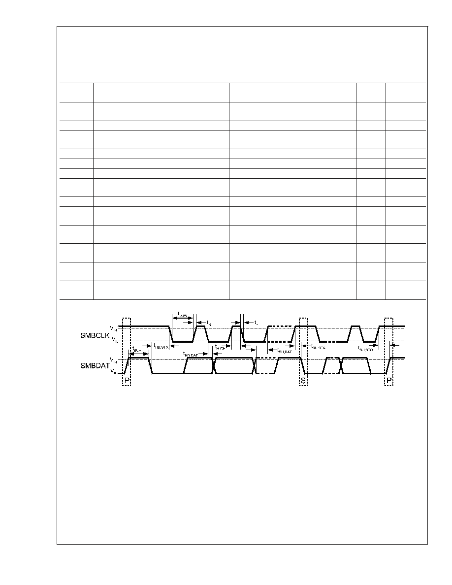
SMBus Digital Switching Characteristics
Unless otherwise noted, these specifications apply for V
DD
= +3.0 VDC to +3.6 VDC, C
L
(load capacitance) on output lines =
80 pF. Boldface limits apply for T
A
= T
J
; T
MIN
T
A
T
MAX
; all other limits T
A
= T
J
= +25įC, unless otherwise noted. The
switching characteristics of the LM63 fully meet or exceed the published specifications of the SMBus version 2.0. The following
parameters are the timing relationships between SMBCLK and SMBDAT signals related to the LM63. They adhere to but are
not necessarily the same as the SMBus bus specifications.
Symbol
Parameter
Conditions
Limits
(Note 8)
Units
(Limit)
f
SMB
SMBus Clock Frequency
10
100
kHz (min)
kHz (max)
t
LOW
SMBus Clock Low Time
From V
IN(0) max
to V
IN(0) max
4.7
Ķs (min)
t
HIGH
SMBus Clock High Time
From V
IN(1) min
to V
IN(1) min
4.0
50
Ķs (min)
Ķs (max)
t
R
SMBus Rise Time
(Note 11)
1
Ķs (max)
t
F
SMBus Fall Time
(Note 12)
0.3
Ķs (max)
t
OF
Output Fall Time
C
L
= 400 pF, I
O
= 3 mA
250
ns (max)
t
TIMEOUT
SMBData and SMBCLK Time Low for Reset
of Serial Interface See (Note 13)
25
35
ms (min)
ms (max)
t
SU:DAT
Data In Setup Time to SMBCLK High
250
ns (min)
t
HD:DAT
Data Out Hold Time after SMBCLK Low
300
930
ns (min)
ns (max)
t
HD:STA
Hold Time after (Repeated) Start Condition.
After this period the first clock is generated.
4.0
Ķs (min)
t
SU:STO
Stop Condition SMBCLK High to SMBDAT
Low (Stop Condition Setup)
100
ns (min)
t
SU:STA
SMBus Repeated Start-Condition Setup Time,
SMBCLK High to SMBDAT Low
4.7
Ķs (min)
t
BUF
SMBus Free Time between Stop and Start
Conditions
4.7
Ķs (min)
20057004
SMBus Timing Diagram for SMBCLK and SMBDAT Signals
LM63
www.national.com
6
Note 1: Absolute Maximum Ratings indicate limits beyond which damage to the device may occur. Operating Ratings indicate conditions for which the device is
functional, but do not guarantee performance limits. For guaranteed specifications and test conditions, see the Electrical Characteristics. The guaranteed
specifications apply only for the test conditions listed. Some performance characteristics may degrade when the device is not operated under the listed test
conditions.
Note 2: All voltages are measured with respect to GND, unless otherwise noted.
Note 3: When the input voltage (V
IN
) at any pin exceeds the power supplies (V
IN
<
GND or V
IN
>
V+), the current at that pin should be limited to 5 mA. Parasitic
components and/or ESD protection circuitry are shown below for the LM63's pins. The nominal breakdown voltage of D3 is 6.5 V. Care should be taken not to forward
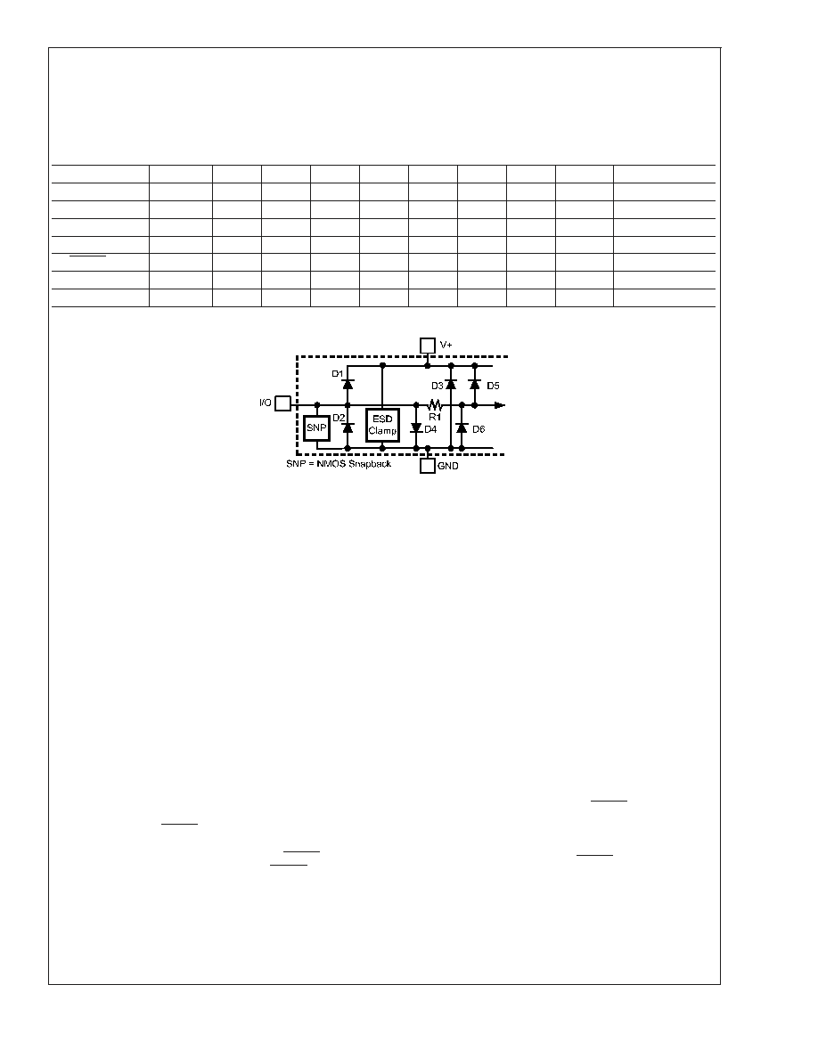
bias the parasitic diode, D1, present on pins D+ and D-. Doing so by more than 50 mV may corrupt temperature measurements. An "X" means it exists in the circuit.
Pin Name
PIN #
D1
D2
D3
D4
D5
D6
R1
SNP
ESD CLAMP
V
DD
1
X
X
D+
2
X
X
X
X
X
X
D-
3
X
X
X
X
X
X
PWM
4
X
X
X
X
ALERT/Tach
6
X
X
X
X
SMBDAT
7
X
X
X
X
SMBCLK
8
X
X
Note 4: Human body model, 100 pF discharged through a 1.5 k
resistor. Machine model, 200 pF discharged directly into each pin. See Figure 1 above for the ESD
Protection Input Structure.
Note 5: Thermal resistance junction-to-ambient when attached to a printed circuit board with 2 oz. foil is 168įC/W.
Note 6: See the URL "http://www.national.com/packaging/" for other recommendations and methods of soldering surface mount devices.
Note 7: "Typicals" are at T
A
= 25įC and represent most likely parametric norm. They are to be used as general reference values not for critical design calculations.
Note 8: Limits are guaranteed to National's AOQL (Average Outgoing Quality Level).
Note 9: The supply current will not increase substantially with an SMBus transaction.
Note 10: Local temperature accuracy does not include the effects of self-heating. The rise in temperature due to self-heating is the product of the internal power
dissipation of the LM63 and the thermal resistance. See (Note 5) for the thermal resistance to be used in the self-heating calculation.
Note 11: The output rise time is measured from (V
IL max
- 0.15 V) to (V
IH min
+ 0.15 V).
Note 12: The output fall time is measured from (V
IH min
+ 0.15 V) to (V
IL min
- 0.15 V).
Note 13: Holding the SMBData and/or SMBCLK lines Low for a time interval greater than t
TIMEOUT
will reset the LM63's SMBus state machine, therefore setting
SMBDAT and SMBCLK pins to a high impedance state.
1.0 Functional Description
The LM63 Remote Diode Temperature Sensor with Inte-
grated Fan Control incorporates a
V
BE
-based temperature
sensor using a Local or Remote diode and a 10-bit plus sign
ADC (Delta-Sigma Analog-to-Digital Converter). The
pulse-width modulated (PWM) open-drain output, with a
pull-up resistor, can drive a switching transistor to modulate
the fan. When the ALERT/Tach is programmed to the Tach
mode the LM63 can measure the fan speed on the pulses
from the fan's tachometer output. When the ALERT/Tach pin
is programmed to the ALERT mode the ALERT open-drain
output will be pulled low when the measured temperature
exceeds certain programmed limits when enabled. Details
are contained in the sections below.
The LM63's two-wire interface is compatible with the SMBus
Specification 2.0 . For more information the reader is di-
rected to www.smbus.org.
In the LM63 digital comparators are used to compare the
measured Local Temperature (LT) to the Local High Setpoint
user-programmable temperature limit register. The mea-
sured Remote Temperature (RT) is digitally compared to the
Remote High Setpoint (RHS), the Remote Low Setpoint
(RLS), and the Remote T_CRIT Setpoint (RCS) user-
programmable temperature limits. An ALERT output will oc-
cur when the measured temperature is: (1) higher than either
the High Setpoint or the T_CRIT Setpoint, or (2) lower than
the Low Setpoint. The ALERT Mask register allows the user
to prevent the generation of these ALERT outputs.
The temperature hysteresis is set by the value placed in the
Hysteresis Register (TH).
The LM63 may be placed in a low power Standby mode by
setting the Standby bit found in the Configuration Register. In
the Standby mode continuous conversions are stopped. In
20057005
FIGURE 1. ESD Protection Input Structure
LM63
www.national.com
7
1.0 Functional Description
(Continued)
Standby mode the user may choose to allow the PWM
output signal to continue, or not, by programming the PWM
Disable in Standby bit in the Configuration Register.
The Local Temperature reading and setpoint data registers
are 8-bits wide. The format of the 11-bit remote temperature
data is a 16-bit left justified word. Two 8-bit registers, high
and low bytes, are provided for each setpoint as well as the
temperature reading. Two Remote Temperature Offset
(RTO) Registers: High Byte and Low Byte (RTOHB and
RTOLB) may be used to correct the temperature readings by
adding or subtracting a fixed value based on a different
non-ideality factor of the thermal diode if different from the
0.13
micron
Intel
Pentium
4
or
Mobile
Pentium
4
Processor-M processor's thermal diode. See Section 4.1
Thermal Diode Non-Ideality.
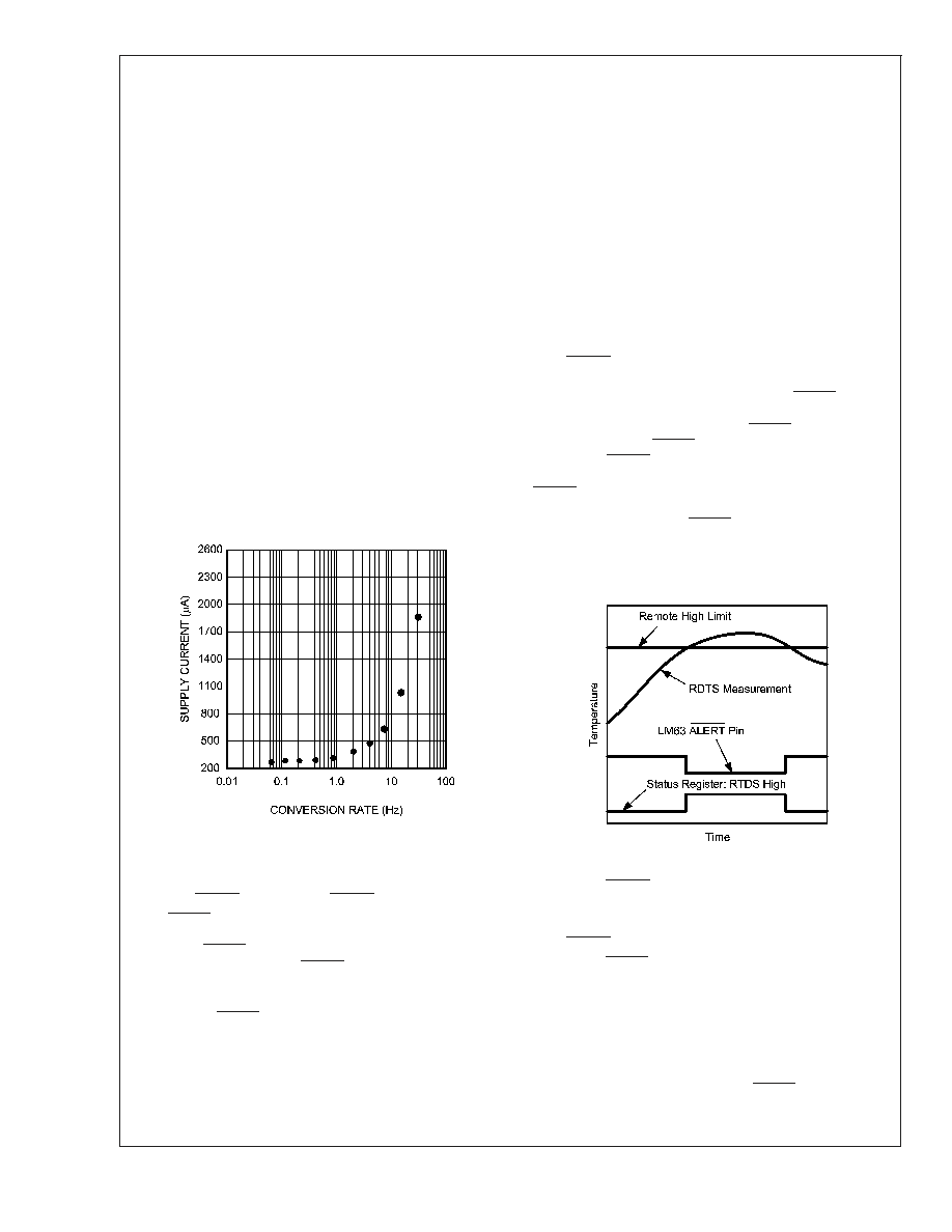
1.1 CONVERSION SEQUENCE
The LM63 takes approximately 31.25 ms to convert the
Local Temperature (LT), Remote Temperature (RT), and to
update all of its registers. The Conversion Rate may be
modified using the Conversion Rate Register. When the
conversion rate is modified a delay is inserted between
conversions,
the
actual
conversion
time
remains
at
31.25 ms. Different Conversion Rates will cause the LM63 to
draw different amounts of supply current as shown in Figure
2.
1.2 THE ALERT/TACH PIN AS ALERT OUTPUT
The ALERT/Tach pin is a multi-use pin. In this section we will
address the ALERT active-low open-drain output function.
When the ALERT/Tach Select bit is written as a zero in the
Configuration Register the ALERT output is selected. Also,
when the ALERT Mask bit in the Configuration register is
written as zero the ALERT interrupts are enabled.
The LM63's ALERT pin is versatile and can produce three
different methods of use to best serve the system designer:
(1) as a temperature comparator (2) as a temperature-based
interrupt flag, and (3) as part of an SMBus ALERT System.
The three methods of use are further described below. The
ALERT and interrupt methods are different only in how the
user interacts with the LM63.
The remote temperature (RT) reading is associated with a
T_CRIT Setpoint Register, and both local and remote tem-
perature (LT and RT) readings are associated with a HIGH
setpoint register (LHS and RHS). The RT is also associated
with a LOW setpoint register (RLS). At the end of every
temperature reading a digital comparison determines
whether that reading is above its HIGH or T_CRIT setpoint or
below its LOW setpoint. If so, the corresponding bit in the
ALERT Status Register is set. If the ALERT mask bit is low,
any bit set in the ALERT Status Register, with the exception
of Busy or Open, will cause the ALERT output to be pulled
low. Any temperature conversion that is out of the limits
defined in the temperature setpoint registers will trigger an
ALERT. Additionally, the ALERT Mask Bit must be cleared to
trigger an ALERT in all modes.
The three different ALERT modes will be discussed in the
following sections.
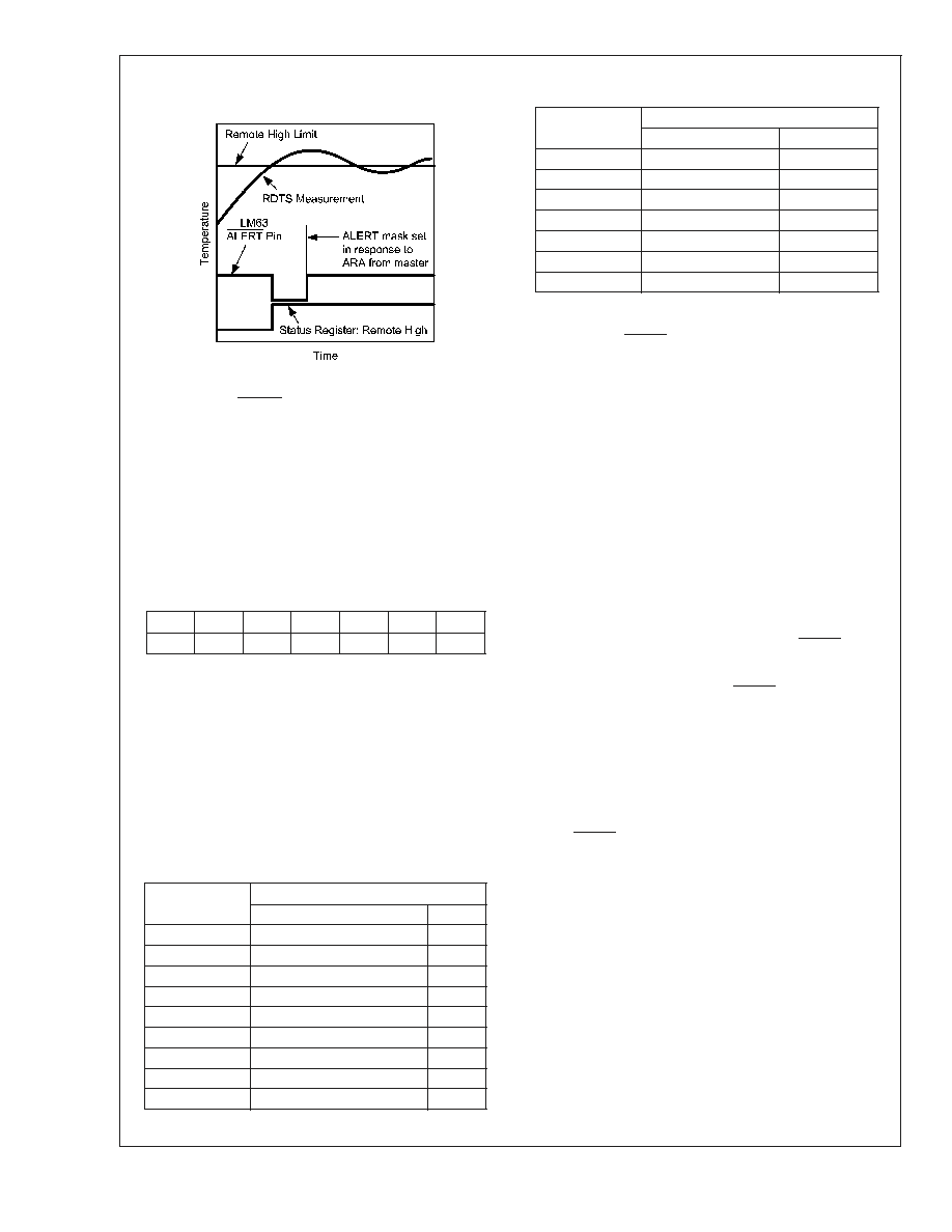
1.2.1 ALERT Output as a Temperature Comparator
When the LM63 is used in a system in which does not
require temperature-based interrupts, the ALERT output
could be used as a temperature comparator. In this mode,
once the condition that triggered the ALERT to go low is no
longer present, the ALERT is negated (Figure 3). For ex-
ample, if the ALERT output was activated by the comparison
of LT
>
LHS, when this condition is no longer true, the
ALERT will return HIGH. This mode allows operation without
software intervention, once all registers are configured dur-
ing set-up. In order for the ALERT to be used as a tempera-
ture comparator, the Comparator Mode bit in the Remote
Diode Temperature Filter and Comparator Mode Register
must be asserted. This is not the power-on default state.
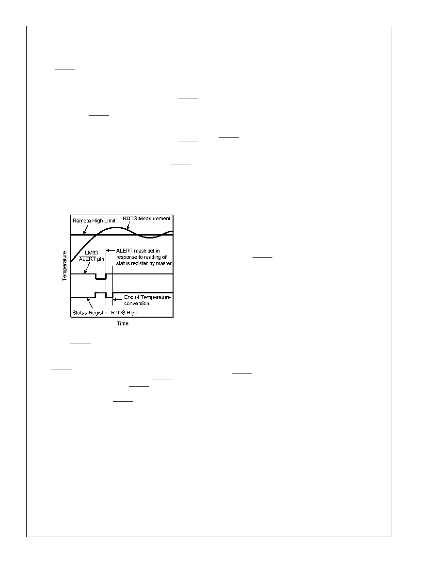
1.2.2 ALERT Output as an Interrupt
The LM63's ALERT output can be implemented as a simple
interrupt signal when it is used to trigger an interrupt service
routine. In such systems it is desirable for the interrupt flag to
repeatedly trigger during or before the interrupt service rou-
tine has been completed. Under this method of operation,
during the read of the ALERT Status Register the LM63 will
set the ALERT Mask bit in the Configuration Register if any
bit in the ALERT Status Register is set, with the exception of
Busy and Open. This prevents further ALERT triggering until
the master has reset the ALERT Mask bit, at the end of the
interrupt service routine. The ALERT Status Register bits are
20057006
FIGURE 2. Supply Current vs Conversion Rate
20057007
FIGURE 3. ALERT Output as Temperature Comparator
Response Diagram
LM63
www.national.com
8
1.0 Functional Description
(Continued)
cleared only upon a read command from the master (see
Figure 4 ) and will be re-asserted at the end of the next
conversion if the triggering condition(s) persist(s). In order
for the ALERT to be used as a dedicated interrupt signal, the
Comparator Mode bit in the Remote Diode Temperature
Filter and Comparator Mode Register must be set low. This
is the power-on default state. The following sequence de-
scribes the response of a system that uses the ALERT
output pin as an interrupt flag:
1.
Master senses ALERT low.
2.
Master reads the LM63 ALERT Status Register to deter-
mine what caused the ALERT.
3.
LM63 clears ALERT Status Register, resets the ALERT
HIGH and sets the ALERT Mask bit in the Configuration
Register.
4.
Master attends to conditions that caused the ALERT to
be triggered. The fan is started, setpoint limits are ad-
justed, etc.
5.
Master resets the ALERT Mask bit in the Configuration
Register.
1.2.3 ALERT Output as an SMBus ALERT
An SMBus alert line is created when the ALERT output is
connected to: (1) one or more ALERT outputs of other
SMBus compatible devices, and (2) to a master. Under this
implementation, the LM63's ALERT should be operated us-
ing the ARA (Alert Response Address) protocol. The SMBus
2.0 ARA protocol, defined in the SMBus specification 2.0, is
a procedure designed to assist the master in determining
which part generated an interrupt and to service that inter-
rupt.
The SMBus alert line is connected to the open-drain ports of
all devices on the bus, thereby AND'ing them together. The
ARA method allows the SMBus master, with one command,
to identify which part is pulling the SMBus alert line LOW. It
also prevents the part from pulling the line LOW again for the
same triggering condition. When an ARA command is re-
ceived by all devices on the bus, the devices pulling the
SMBus alert line LOW: (1) send their address to the master
and (2) release the SMBus alert line after acknowledgement
of their address.
The SMBus Specifications 1.1 and 2.0 state that in response
to and ARA (Alert Response Address) "after acknowledging
the slave address the device must disengage its ALERT
pulldown". Furthermore, "if the host still sees ALERT low
when the message transfer is complete, it knows to read the
ARA again." This SMBus "disengaging ALERT requirement
prevents locking up the SMBus alert line. Competitive parts
may address the "disengaging of ALERT" differently than the
LM63 or not at all. SMBus systems that implement the ARA
protocol as suggested for the LM63 will be fully compatible
with all competitive parts.
The LM63 fulfills "disengaging of ALERT" by setting the
ALERT Mask Bit in the Configuration Register after sending
out its address in response to an ARA and releasing the
ALERT output pin. Once the ALERT Mask bit is activated,
the ALERT output pin will be disabled until enabled by
software. In order to enable the ALERT the master must read
the ALERT Status Register, during the interrupt service rou-
tine and then reset the ALERT Mask bit in the Configuration
Register to 0 at the end of the interrupt service routine.
The following sequence describes the ARA response proto-
col.
1.
Master senses SMBus alert line low
2.
Master sends a START followed by the Alert Response
Address (ARA) with a Read Command.
3.
Alerting Device(s) send ACK.
4.
Alerting Device(s) send their address. While transmitting
their address, alerting devices sense whether their ad-
dress has been transmitted correctly. (The LM63 will
reset its ALERT output and set the ALERT Mask bit once
its complete address has been transmitted successfully.)
5.
Master/slave NoACK
6.
Master sends STOP
7.
Master attends to conditions that caused the ALERT to
be triggered. The ALERT Status Register is read and fan
started, setpoints adjusted, etc.
8.
Master resets the ALERT Mask bit in the Configuration
Register.
The ARA, 000 1100, is a general call address. No device
should ever be assigned to this address.
The ALERT Configuration bit in the Remote Diode Tempera-
ture Filter and Comparator Mode Register must be set low in
order for the LM63 to respond to the ARA command.
The ALERT output can be disabled by setting the ALERT
Mask bit in the Configuration Register. The power-on default
is to have the ALERT Mask bit and the ALERT Configuration
bit low.
20057008
FIGURE 4. ALERT Output as an Interrupt Temperature
Response Diagram
LM63
www.national.com
9
1.0 Functional Description
(Continued)
1.3 SMBus INTERFACE
Since the LM63 operates as a slave on the SMBus the
SMBCLK line is an input and the SMBDAT line is bi-
directional. The LM63 never drives the SMBCLK line and it
does not support clock stretching. According to SMBus
specifications, the LM63 has a 7-bit slave address. All bits,
A6 through A0, are internally programmed and cannot be
changed by software or hardware.
The complete slave address is:
A6
A5
A4
A3
A2
A1
A0
1
0
0
1
1
0
0
1.4 POWER-ON RESET (POR) DEFAULT STATES
For information on the POR default states see Section 2.2
LM63 Register Map in Functional Order.
1.5 TEMPERATURE DATA FORMAT
Temperature data can only be read from the Local and
Remote Temperature registers. The High, Low and T_CRIT
setpoint registers are Read/Write.
Remote temperature data is represented by an 11-bit, two's
complement word with a Least Significant Bit (LSB) equal to
0.125įC. The data format is a left justified 16-bit word avail-
able in two 8-bit registers:
Temperature
Digital Output
Binary
Hex
+125įC
0111 1101 0000 0000
7D00
+25įC
0001 1001 0000 0000
1900
+1įC
0000 0001 0000 0000
0100
+0.125įC
0000 0000 0010 0000
0020
0įC
0000 0000 0000 0000
0000
-0.125įC
1111 1111 1110 0000
FFE0
-1įC
1111 1111 0000 0000
FF00
-25įC
1110 0111 0000 0000
E700
-55įC
1100 1001 0000 0000
C900
Local Temperature data is represented by an 8-bit, two's
complement byte with an LSB equal to 1įC:
Temperature
Digital Output
Binary
Hex
+125įC
0111 1101
7D
+25įC
0001 1001
19
+1įC
0000 0001
01
0įC
0000 0000
00
-1įC
1111 1111
FF
-25įC
1110 0111
E7
-55įC
1100 1001
C9
1.6 OPEN-DRAIN OUTPUTS
The SMBDAT, ALERT, and PWM outputs are open-drain
outputs and do not have internal pull-ups. A "High" level will
not be observed on these pins until pull-up current is pro-
vided by an internal source, typically through a pull-up resis-
tor. Choice of resistor value depends on several factors but,
in general, the value should be as high as possible consis-
tent with reliable operation. This will lower the power dissi-
pation of the LM63 and avoid temperature errors caused by
self-heating of the device. The maximum value of the pull-up
resistor to provide the 2.1 V high level is 88.7 k
.
1.7 DIODE FAULT DETECTION
The LM63 can detect fault conditions caused by the remote
diode. If the D+ pin is detected to be shorted to V
DD
, or open:
(1) the Remote Temperature High Byte (RTHB) register is
loaded with 127įC, (2) the Remote Temperature Low Byte
(RTLB) register is loaded with 0, and (3) the OPEN bit (D2)
in the status register is set. Therefore, if the Remote T_CRIT
setpoint register (RCS): (1) is set to a value less than +127įC
and (2) the ALERT Mask is disabled, then the ALERT output
pin will be pulled low. If the Remote High Setpoint High Byte
(RHSHB) is set to a value less than +127įC and (2) the
ALERT Mask is disabled, then the ALERT will be pulled low.
The OPEN bit by itself will not trigger an ALERT.
If the D+ pin is shorted to either ground or D-, then the
Remote Temperature High Byte (RTHB) register is loaded
with -128įC (1000 0000) and the OPEN bit in the ALERT
Status Register will not be set. A temperature reading of
-128įC indicates that D+ is shorted to either ground or D-. If
the value in the Remote Low Setpoint High Byte (RLSHB)
Register is more than -128įC and the ALERT Mask is Dis-
abled, ALERT will be pulled low.
1.8 COMMUNICATING WITH THE LM63
Each data register in the LM63 falls into one of four types of
user accessibility:
1.
Read Only
2.
Write Only
3.
Read/Write same address
4.
Read/Write different address
A Write to the LM63 is comprised of an address byte and a
command byte. A write to any register requires one data
byte.
Reading the LM63 Registers can take place after the requi-
site register setup sequence takes place. See Section 2.1.1
LM63 Required Initial Fan Control Register Sequence.
The data byte has the Most Significant Bit (MSB) first. At the
end of a read, the LM63 can accept either Acknowledge or
20057009
FIGURE 5. ALERT Output as an SMBus ALERT
Temperature Response Diagram
LM63
www.national.com
10
1.0 Functional Description
(Continued)
No-Acknowledge from the Master. Note that the No-
Acknowledge is typically used as a signal for the slave
indicating that the Master has read its last byte.
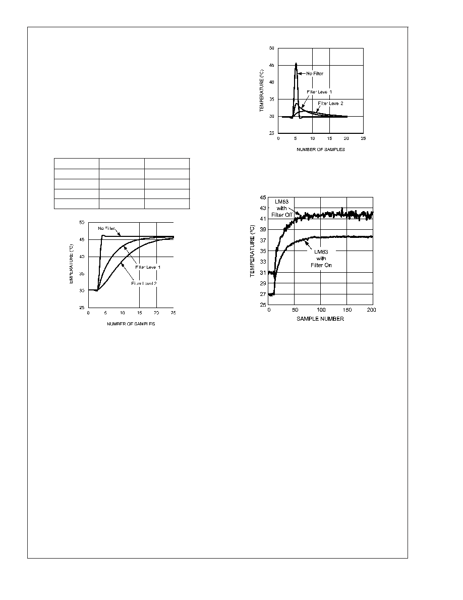
1.9 DIGITAL FILTER
The LM63 incorporates a user-configured digital filter to
suppress erroneous Remote Temperature readings due to
noise. The filter is accessed in the Remote Diode Tempera-
ture Filter and Comparator Mode Register. The filter can be
set according to the following table.
Level 2 is maximum filtering.
Digital Filter Selection Table
D2
D1
Filter
0
0
No Filter
0
1
Level 1
1
0
Level 1
1
1
Level 2
20057010
FIGURE 6. Step Response of the Digital Filter
20057011
FIGURE 7. Impulse Response of the Digital Filter
20057012
FIGURE 8. Digital Filter Response in an Intel Pentium 4
processor System. The Filter on and off curves were
purposely offset to better show noise performance.
LM63
www.national.com
11
1.0 Functional Description
(Continued)
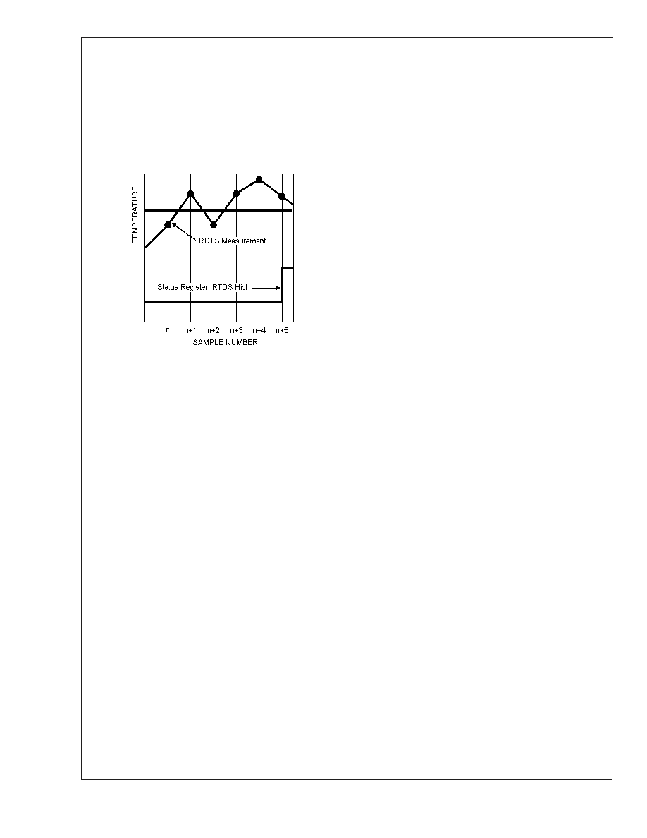
1.10 FAULT QUEUE
The LM63 incorporates a Fault Queue to suppress errone-
ous ALERT triggering . The Fault Queue prevents false
triggering by requiring three consecutive out-of-limit HIGH,
LOW, or T_CRIT temperature readings. See Figure 9. The
Fault Queue defaults to OFF upon power-up and may be
activated by setting the RDTS Fault Queue bit in the Con-
figuration Register to a 1.
1.11 ONE-SHOT REGISTER
The One-Shot Register is used to initiate a single conversion
and comparison cycle when the device is in standby mode,
after which the data returns to standby. This is not a data
register. A write operation causes the one-shot conversion.
The data written to this address is irrelevant and is not
stored. A zero will always be read from this register.
1.12 SERIAL INTERFACE RESET
In the event that the SMBus Master is reset while the LM63
is transmitting on the SMBDAT line, the LM63 must be
returned to a known state in the communication protocol.
This may be done in one of two ways:
1.
When SMBDAT is Low, the LM63 SMBus state machine
resets to the SMBus idle state if either SMBData or
SMBCLK are held Low for more than 35 ms (t
TIMEOUT
).
All devices are to timeout when either the SMBCLK or
SMBDAT lines are held Low for 25 ms ≠ 35 ms. There-
fore, to insure a timeout of all devices on the bus, either
the SMBCLK or the SMBData line must be held Low for
at least 35 ms.
2.
With both SMBDAT and SMBCLK High, the master can
initiate an SMBus start condition with a High to Low
transition on the SMBDAT line. The LM63 will respond
properly to an SMBus start condition at any point during
the communication. After the start the LM63 will expect
an SMBus Address address byte.
20057013
FIGURE 9. Fault Queue Temperature Response
Diagram
LM63
www.national.com
12
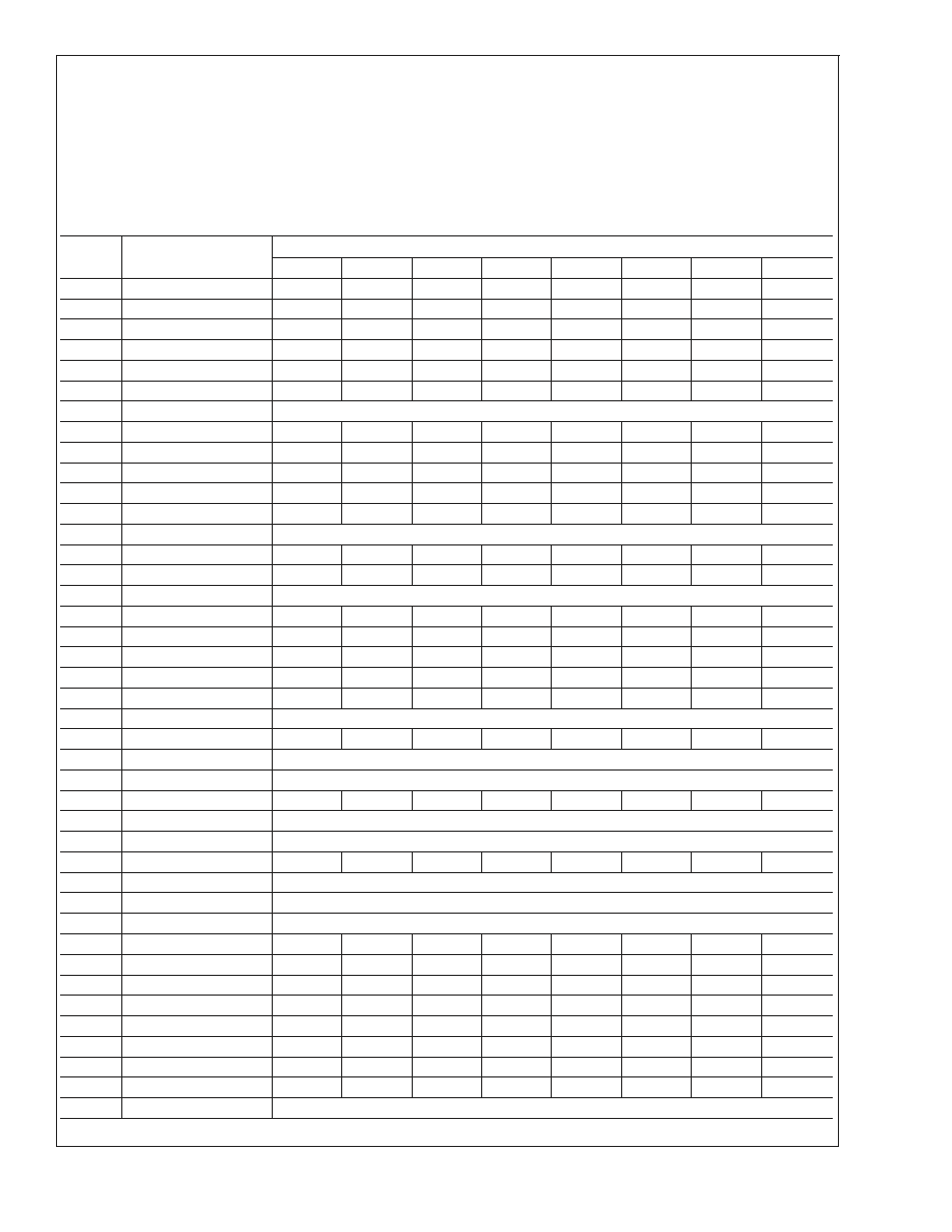
2.0 LM63 Registers
The following pages include: Section 2.1, a Register Map in Hexadecimal Order, which shows a summary of all registers and their
bit assignments, Section 2.2, a Register Map in Functional Order, and Section 2.3, a detailed explanation of each register. Do not
address the unused or manufacturer's test registers.
2.1 LM63 REGISTER MAP IN HEXADECIMAL ORDER
The following is a Register Map grouped in hexadecimal address order. Some address locations have been left blank to maintain
compatibility with LM86. Addresses in parenthesis are mirrors of "Same As" address for backwards compatibility with some older
software. Reading or writing either address will access the same 8-bit register.
Register
0x[HEX]
Register Name
DATA BITS
D7
D6
D5
D4
D3
D2
D1
D0
00
Local Temperature
LT7
LT6
LT5
LT4
LT3
LT2
LT1
LT0
01
Rmt Temp MSB
RTHB
Ī
RTHB14
RTHB13
RTHB12
RTHB11
RTHB10
RTHB9
RTHB8
02
ALERT Status
BUSY
LHIGH
0
RHIGH
RLOW
RDFA
RCRIT
TACH
03
Configuration
ALTMSK
STBY
PWMDIS
0
0
ALT/TCH
TCRITOV
FLTQUE
04
Conversion Rate
0
0
0
0
CONV3
CONV2
CONV1
CONV0
05
Local High Setpoint
LHS7
LHS6
LHS5
LHS4
LHS3
LHS2
LHS1
LHS0
06
[Reserved]
Not Used
07
Rmt High Setpoint MSB RHSHB15 RHSHB14 RHHBS13 RHSHB12 RHSHB11 RHSHB10
RHSHB9
RHSHB8
08
Rmt Low Setpoint MSB
RLSHB15 RLSHB14 RLSHB13 RLSHB12
RLHBS11
RLSHB10
RLSHB9
RLSHB8
(09)
Same as 03
(0A)
Same as 04
(0B)
Same as 05
0C
[Reserved]
Not Used
(0D)
Same as 07
(0E)
Same as 08
0F
One Shot
Write Only. Write command triggers one temperature conversion cycle.
10
Rmt Temp LSB
RTLB7
RTLB6
RTLB5
0
0
0
0
0
11
Rmt Temp Offset MSB
RTOHB15 RTOHB14 RTOHB13 RTOHB12 RTOHB11 RTOHB10
RTOHB9
RTOHB8
12
Rmt Temp Offset LSB
RTOLB7
RTOLB6
RTOLB5
0
0
0
0
0
13
Rmt High Setpoint LSB
RHSLB7
RHSLB6
RHSLB5
0
0
0
0
0
14
Rmt Low Setpoint LSB
RLSLB7
RLSLB6
RLSLB5
0
0
0
0
0
15
[Reserved]
Not Used
16
ALERT Mask
1
ALTMSK6
1
ALTMSK4 ALTMSK3
1
ALTMSK1 ALTMSK0
17
[Reserved]
Not Used
18
[Reserved]
Not Used
19
Rmt TCRIT Setpoint
RCS7
RCS6
RCS5
RCS4
RCS3
RCS2
RCS1
RCS0
1A≠1F
[Reserved]
Not Used
20
[Reserved]
Not Used
21
Rmt TCRIT Hysteresis
RTH7
RTH6
RTH5
RTH4
RTH3
RTH2
RTH1
RTH0
22≠2F
[Reserved]
Not Used
30≠3F
[Reserved]
Not Used
40≠45
[Reserved]
Not Used
46
Tach Count LSB
TCLB5
TCLB4
TCLB3
TCLB2
TCLB1
TCLB0
TEDGE1
TEDGE0
47
Tach Count MSB
TCHB13
TCHB12
TCHB11
TCHB10
TCHB9
TCHB8
TCHB7
TCHB6
48
Tach Limit LSB
TLLB7
TLLB6
TLLB5
TLLB4
TLLB3
TLLB2
Not Used
Not Used
49
Tach Limit MSB
TLHB15
TLHB14
TLHB13
TLHB12
TLHB11
TLHB10
TLHB9
TLHB8
4A
PWM and RPM
0
0
PWPGM
PWOUT
Ī
PWCKSL
0
TACH1
TACH0
4B
Fan Spin-Up Config
0
0
SPINUP
SPNDTY1 SPNDTY0 SPNUPT2 SPNUPT1 SPNUPT0
4C
PWM Value
0
0
PWVAL5
PWVAL4
PWVAL3
PWVAL2
PWVAL1
PWVAL0
4D
PWM Frequency
0
0
0
PWMF4
PWMF3
PWMF2
PWMF1
PWMF0
4E
[Reserved]
Not Used
LM63
www.national.com
13
2.0 LM63 Registers
(Continued)
Register
0x[HEX]
Register Name
DATA BITS
D7
D6
D5
D4
D3
D2
D1
D0
4F
Lookup Table Hystersis
0
0
0
LOOKH4
LOOKH3
LOOKH2
LOOKH1
LOOKH0
50≠5F
Lookup Table
Lookup Table of up to 8 PWM and Temp Pairs in 8-bit Registers
60≠BE
[Reserved]
Not Used
BF
Rmt Diode Temp Filter
0
0
0
0
0
RDTF1
RDTF0
ALTCOMP
C0≠FD
[Reserved]
Not Used
FE
Manufacturer's ID
0
0
0
0
0
0
0
1
FF
Stepping/Die Rev. ID
0
1
0
0
0
0
0
1
2.2 LM63 REGISTER MAP IN FUNCTIONAL ORDER
The following is a Register Map grouped in Functional Order. Some address locations have been left blank to maintain
compatibility with LM86. Addresses in parenthesis are mirrors of named address. Reading or writing either address will access
the same 8-bit register. The Fan Control and Configuration Registers are listed first, as there is a required order to setup these
registers first and then setup the others. The detailed explanations of each register will follow the order shown below. POR =
Power-On-Reset.
Register
[HEX]
Register Name
Read/Write
POR Default
[HEX]
FAN CONTROL REGISTERS
4A
PWM and RPM
R/W
20
4B
Fan Spin-Up Configuration
R/W
3F
4D
PWM Frequency
R/W
17
4C
PWM Value
Read Only
(R/W if Override Bit is Set)
00
50≠5F
Lookup Table
R/W
See Table
4F
Lookup Table Hysteresis
R/W
04
CONFIGURATION REGISTER
03 (09)
Configuration
R/W
00
TACHOMETER COUNT AND LIMIT REGISTERS
46
Tach Count LSB
Read Only
N/A
47
Tach Count MSB
Read Only
N/A
48
Tach Limit LSB
R/W
FF
49
Tach Limit MSB
R/W
FF
LOCAL TEMPERATURE AND LOCAL SETPOINT REGISTERS
00
Local Temperature
Read Only
N/A
05 (0B)
Local High Setpoint
R/W
46 (70į)
REMOTE DIODE TEMPERATURE AND SETPOINT REGISTERS
01
Remote Temperature MSB
Read Only
N/A
10
Remote Temperature LSB
Read Only
N/A
11
Remote Temperature Offset MSB
R/W
00
12
Remote Temperature Offset LSB
R/W
00
07 (0D)
Remote High Setpoint MSB
R/W
46 (70įC)
13
Remote High Setpoint LSB
R/W
00
08 (0E)
Remote Low Setpoint MSB
R/W
00 (0įC)
14
Remote Low Setpoint LSB
R/W
00
19
Remote TCRIT Setpoint
R/W
55 (85įC)
21
Remote TCRIT Hys
R/W
0A (10įC)
BF
Remote Diode Temperature Filter
R/W
00
CONVERSION AND ONE-SHOT REGISTERS
04 (0A)
Conversion Rate
R/W
08
0F
One-Shot
Write Only
N/A
LM63
www.national.com
14
2.0 LM63 Registers
(Continued)
Register
[HEX]
Register Name
Read/Write
POR Default
[HEX]
ALERT STATUS AND MASK REGISTERS
02
ALERT Status
Read Only
N/A
16
ALERT Mask
R/W
A4
ID AND TEST REGISTERS
FF
Stepping/Die Rev. ID
Read Only
41
[RESERVED] REGISTERS -- NOT USED
06
Not Used
N/A
N/A
0C
Not Used
N/A
N/A
15
Not Used
N/A
N/A
17
Not Used
N/A
N/A
18
Not Used
N/A
N/A
1A≠1F
Not Used
N/A
N/A
20
Not Used
N/A
N/A
22≠2F
Not Used
N/A
N/A
30≠3F
Not Used
N/A
N/A
40≠45
Not Used
N/A
N/A
4E
Not Used
N/A
N/A
60≠BE
Not Used
N/A
N/A
C0≠FD
Not Used
N/A
N/A
2.3 LM63 INITIAL REGISTER SEQUENCE AND REGISTER DESCRIPTIONS IN FUNCTIONAL ORDER
The following is a Register Map grouped in functional and sequence order. Some address locations have been left blank to
maintain compatibility with LM86. Addresses in parenthesis are mirrors of named address for backwards compatibility with some
older software. Reading or writing either address will access the same 8-bit register.
2.3.1 LM63 Required Initial Fan Control Register Sequence
Important! The BIOS must follow the sequence below to configure the following Fan Registers for the LM63 before using any of
the Fan or Tachometer or PWM registers:
Step
[Register]
HEX
and Setup Instructions
1
[4A] Write bits 0 and 1; 3 and 4. This includes tach settings if used, PWM internal clock select (1.4 kHz or
360 kHz) and PWM Output Polarity.
2
[4B] Write bits 0 through 5 to program the spin-up settings.
3
[4D] Write bits 0 through 4 to set the frequency settings. This works with the PWM internal clock select.
4
Choose, then write, only one of the following:
A. [4F≠5F] the Lookup Table, or
B. [4C] the PWM value bits 0 through 5.
5
If Step 4A, Lookup Table, was chosen and written then write [4A] bit 5 = 0.
All other registers can be written at any time after the above sequence.
LM63
www.national.com
15
2.0 LM63 Registers
(Continued)
LM63 Register Descriptions In Functional Order
Fan Control Registers
Address
Hex
Read/
Write
Bits
POR
Value
Name
Description
4A
HEX
FAN PWM AND TACHOMETER CONFIGURATION REGISTER
4A
R/W
7:6
00
PWM
Program
These bits are unused and always set to 0.
5
1
0: the PWM Value (register 4C) and the Lookup Table (50≠5F) are
read-only. The PWM value (0 to 100%) is determined by the current
remote diode temperature and the Lookup Table, and can be read from
the PWM value register.
1: the PWM value (register 4C) and the Lookup Table (Register 50≠5F)
are read/write enabled. Writing the PWM Value register will set the
PWM output. This is also the state during which the Lookup Table can
be written.
4
0
PWM
Output
Polarity
0: the PWM output pin will be 0 V for fan OFF and open for fan ON.
1: the PWM output pin will be open for fan OFF and 0 V for fan ON.
3
0
PWM Clock
Select
if 0, the master PWM clock is 360 kHz
if 1, the master PWM clock is 1.4 kHz.
2
0
[Reserved]
Always write 0 to this bit.
1:0
00
Tachometer
Mode
00: Traditional tach input monitor, false readings when under minimum
detectable RPM.
01: Traditional tach input monitor, FFFF reading when under minimum
detectable RPM.
10: Most accurate readings, FFFF reading when under minimum
detectable RPM.
11: Least effort on programmed PWM of fan, FFFF reading when under
minimum detectable RPM.
Note: If the PWM Clock is 360 kHz, mode 00 is used regardless of the
setting of these two bits.
LM63
www.national.com
16
2.0 LM63 Registers
(Continued)
Fan Control Registers
(Continued)
Address
Hex
Read/
Write
Bits
POR
Value
Name
Description
4B
HEX
FAN PWM AND TACHOMETER CONFIGURATION REGISTER
4B
R/W
7:6
0
Fast
Tachometer
Spin-Up
These bits are unused and always set to 0
5
1
If 0, the fan spin-up uses the duty cycle and spin-up time, bits 0≠4.
If 1, the LM63 sets the PWM output to 100% until the spin-up times out
(per bits 0≠2) or the minimum desired RPM has been reached (per the
Tachometer Setpoint setting) using the tachometer input, whichever
happens first. This bit overrides the PWM Spin-Up Duty Cycle register
(bits 4:3) -- PWM output is always 100%. Register x03, bit 2 = 1 for
Tachometer mode.
If PWM Spin-Up Time (bits 2:0) = 000, the Spin-Up cycle is bypassed,
regardless of the state of this bit.
4:3
11
PWM
Spin-Up
Duty Cycle
00: Spin-Up cycle bypassed (no Spin-Up), unless Fast Tachometer
Terminated Spin-Up (bit 5) is set.
01: 50%
10: 75%≠81% Depends on PWM Frequency. See Applications Notes.
11: 100%
2:0
111
PWM
Spin-Up
Time
000: Spin-Up cycle bypassed (No Spin-Up)
001: 0.05 seconds
010: 0.1 s
011: 0.2 s
100: 0.4 s
101: 0.8 s
110: 1.6 s
111: 3.2 s
4D
HEX
FAN PWM FREQUENCY REGISTER
4D
R/W
7:5
000
PWM
Frequency
These bits are unused and always set to 0
4:0
10111
The PWM Frequency = PWM_Clock / 2n, where PWM_Clock = 360
kHz or 1.4 kHz (per the PWM Clock Select bit in Register 4A), and n =
value of the register. Note: n = 0 is mapped to n = 1. See the
Application Note at the end of this datasheet.
4C
HEX
PWM VALUE REGISTER
4C
Read
(Write
only if
reg
4A bit
5 = 1.)
7:6
00
PWM
Value
These bits are unused and always set to 0
5:0
000000
If PWM Program (register 4A, bit 5) = 0 this register is read only and
reflects the LM63's current PWM value from the Lookup Table.
If PWM Program (register 4A, bit 5) = 1, this register is read/write and
the desired PWM value is written directly to this register, instead of
from the Lookup Table, for direct fan speed control.
This register will read 0 during the Spin-Up cycle.
See Application Notes section at the end of this datasheet for more
information regarding the PWM Value and Duty Cycle in %.
LM63
www.national.com
17
2.0 LM63 Registers
(Continued)
Fan Control Registers
(Continued)
Address
Hex
Read/
Write
Bits
POR
Value
Name
Description
50
HEX
to 5F
HEX
LOOKUP TABLE (7 Bits for Temperature and 6 Bits for PWM for each Temperature/PWM Pair)
50
Read.
(Write
only if
reg
4A bit
5 = 1.)
7
0
Lookup Table
Temperature
Entry 1
This bit is unused and always set to 0.
6:0
0x7F
If the remote diode temperature exceeds this value, the PWM output
will be the value in Register 51.
51
7:6
00
Lookup Table
PWM Entry 1
These bits are unused and always set to 0.
5:0
0x3F
The PWM value corresponding to the temperature limit in register 50.
52
7
0
Lookup Table
Temperature
Entry 2
This bit is unused and always set to 0.
6:0
0x7F
If the remote diode temperature exceeds this value, the PWM output
will be the value in Register 53.
53
7:6
00
Lookup Table
PWM Entry 2
These bits are unused and always set to 0.
5:0
0x3F
The PWM value corresponding to the temperature limit in register 52.
54
7
0
Lookup Table
Temperature
Entry 3
This bit is unused and always set to 0.
6:0
0x7F
If the remote diode temperature exceeds this value, the PWM output
will be the value in Register 55.
55
7:6
00
Lookup Table
PWM Entry 3
These bits are unused and always set to 0.
5:0
0x3F
The PWM value corresponding to the temperature limit in register 54.
56
7
0
Lookup Table
Temperature
Entry 4
This bit is unused and always set to 0.
6:0
0x7F
If the remote diode temperature exceeds this value, the PWM output
will be the value in Register 57.
57
7:6
00
Lookup Table
PWM Entry 4
These bits are unused and always set to 0.
5:0
0x3F
The PWM value corresponding to the temperature limit in register 56.
58
7
0
Lookup Table
Temperature
Entry 5
This bit is unused and always set to 0.
6:0
0x7F
If the remote diode temperature exceeds this value, the PWM output
will be the value in Register 59.
59
7:6
00
Lookup Table
PWM Entry 5
These bits are unused and always set to 0.
5:0
0x3F
The PWM value corresponding to the temperature limit in register 58.
5A
7
0
Lookup Table
Temperature
Entry 6
This bit is unused and always set to 0.
6:0
0x7F
If the remote diode temperature exceeds this value, the PWM output
will be the value in Register 5B.
5B
7:6
00
Lookup Table
PWM Entry 6
These bits are unused and always set to 0.
5:0
0x3F
The PWM value corresponding to the temperature limit in register 5A.
5C
7
0
Lookup Table
Temperature
Entry 7
This bit is unused and always set to 0.
6:0
0x7F
If the remote diode temperature exceeds this value, the PWM output
will be the value in Register 5D.
5D
7:6
00
Lookup Table
PWM Entry 7
These bits are unused and always set to 0.
5:0
0x3F
The PWM value corresponding to the temperature limit in register 5C.
5E
7
0
Lookup Table
Temperature
Entry 8
This bit is unused and always set to 0.
6:0
0x7F
If the remote diode temperature exceeds this value, the PWM output
will be the value in Register 5F.
5F
7:6
00
Lookup Table
PWM Entry 8
These bits are unused and always set to 0.
5:0
0x3F
The PWM value corresponding to the temperature limit in register 5E.
4F
HEX
LOOKUP TABLE HYSTERESIS
4F
R/W
7:5
000
Lookup
Table
Hysteresis
These bits are unused and always set to 0
4:0
00100
The amount of hysteresis applied to the Lookup Table. (1 LSB = 1įC).
LM63
www.national.com
18
2.0 LM63 Registers
(Continued)
Configuration Register
ADDRESS
Hex
Read/
Write
Bits
POR
Value
Name
Description
03 (09)
HEX
CONFIGURATION REGISTER
03 (09)
R/W
7
0
ALERT
Mask
When this bit is a 0, ALERT interrupts are enabled.
When this bit is set to a 1, ALERT interrupts are masked, and the
ALERT pin is always in a high impedance (open) state.
6
0
STANDBY
When this bit is a 0, the LM63 is in operational mode, converting,
comparing, and updating the PWM output continuously.
When this bit is a 1, the LM63 enters a low power standby mode.
In STANDBY, continuous conversions are stopped, but a
conversion/comparison cycle may be initiated by writing any value to
register 0x0F. Operation of the PWM output in STANDBY depends on
the setting of bit 5 in this register.
5
0
PWM Disable
in STANDBY
When this bit is a 0, the LM63's PWM output continues to output the
current fan control signal while in STANDBY.
When this bit is a 1, the PWM output is disabled (as defined by the
PWM polarity bit) while in STANDBY.
4:3
00
These bits are unused and always set to 0.
2
0
ALERT/Tach
Select
When this bit is a 0, the ALERT/Tach pin is an open drain ALERT
output.
When this bit is a 1, the ALERT/Tach pin is a high impedance
Tachometer input.
Note that if this bit is set, the function of the ALERT/Tach pin must be
Tach input, so an external ALERT condition will not occur.
1
0
T_CRIT Limit
Override
The T_CRIT limit for the remote diode is nominally 85įC. This value can
be changed once after power-up by first setting this bit to a 1, then
programming a new T_CRIT value into the Remote Diode T_CRIT Limit
(register 0x19). The T_CRIT value can not be changed again except by
cycling power to the LM63.
0
0
RDTS Fault
Queue
0: an ALERT will be generated if any Remote Diode conversion result is
above the Remote High Set Point or below the Remote Low
Setpoint.
1: an ALERT will be generated only if three consecutive Remote Diode
conversions are above the Remote High Set Point or below the
Remote Low Setpoint.
LM63
www.national.com
19
2.0 LM63 Registers
(Continued)
Tachometer Count And Limit Registers
ADDRESS
Hex
Read/
Write
Bits
POR
Value
Name
Description
47
HEX
TACHOMETER COUNT (MSB) and 46
HEX
TACHOMETER COUNT (LSB) REGISTERS (16 bits: Read LSB first to lock
MSB and ensure MSB and LSB are from the same reading)
47
Read
Only
7:0
N/A
Tachometer
Count (MSB)
These registers contain the current 16-bit Tachometer Count, representing
the period of time between tach pulses.
Note that the 16-bit tachometer MSB and LSB are reversed from the
16-bit temperature readings.
46
Read
Only
7:2
N/A
Tachometer
Count (LSB)
Read
Only
1:0
00
Tachometer
Edge Count
Bits
Edges Used
Tach_Count_Multiple
00:
Reserved - do not use
01:
2
4
10:
3
2
11:
5
1
Note: If PWM_Clock_Select = 360 kHz, then Tach_Count_Multiple = 1
regardless of the setting of these bits.
49
HEX
TACHOMETER LIMIT (MSB) and 48
HEX
TACHOMETER LIMIT (LSB) REGISTERS
49
R/W
7:0
0xFF
Tachometer
Limit MSB)
These registers contain the current 16-bit Tachometer Count, representing
the period of time between tach pulses. Fan RPM = (f
*
5,400,000) /
(Tachometer Count), where f = 1 for 2 pulses/rev fan; f = 2 for 1 pulse/rev
fan; and f = 2/3 for 3 pulses/rev fan. See the Applications Notes section
for more tachometer information. Note that the 16-bit tachometer MSB and
LSB are reversed from the 16 bit temperature readings.
48
R/W
7:2
0xFF
Tachometer
Limit (LSB)
R/W
1:0
[Reserved]
Not Used.
Local Temperature And Local High Setpoint Registers
ADDRESS
Hex
Read/
Write
Bits
POR
Value
Name
Description
00
HEX
LOCAL TEMPERATURE REGISTER (8-bits)
00
Read
Only
7:0
N/A
Local
Temperature
Reading (8-bit)
8-bit integer representing the temperature of the LM63 die.
05 (0B)
HEX
LOCAL HIGH SETPOINT REGISTER (8-bits)
05
R/W
7:0
0x46
(70į)
Local HIGH
Setpoint
High Setpoint for the internal diode.
LM63
www.national.com
20
2.0 LM63 Registers
(Continued)
Remote Diode Temperature, Offset And Setpoint Registers
ADDRESS
Hex
Read/
Write
Bits
POR
Value
Name
Description
01
Read
Only
7:0
N/A
Remote Diode
Temperature
Reading (MSB)
This is the MSB of the 2's complement value, representing the
temperature of the remote diode connected to the LM63. Bit 7 is the sign
bit, bit 6 has a weight of 0x40 (64į), and bit 0 has a weight of 1įC. This
byte to be read first.
10
Read
Only
7:5
N/A
Remote Diode
Temperature
Reading (MSB)
This is the LSB of the 2's complement value, representing the
temperature of the remote diode connected to the LM63. Bit 7 has a
weight 0.5įC, bit 6 has a weight of 0.25įC, and bit 5 has a weight of
0.125įC.
4:0
00
Always 00.
11
R/W
7:5
00
Remote
Temperature
OFFSET (MSB)
These registers contain the value added to or subtracted from the
remote diode's reading to compensate for the different non-ideality
factors of different processors, diodes, etc. The 2's complement value, in
these registers is added to the output of the LM63's ADC to form the
temperature reading contained in registers 01 and 10.
12
R/W
7:5
00
Remote
Temperature
OFFSET (LSB)
4:0
00
Always 00.
07 (0D)
R/W
7:0
0x46
(70įC)
Remote HIGH
Setpoint (MSB)
High setpoint temperature for remote diode. Same format as Remote
Temperature Reading (registers 01 and 10).
13
R/W
7:5
00
Remote HIGH
Setpoint (LSB)
4:0
00
Always 00.
08 (0E)
R/W
7:0
00
(0įC)
Remote LOW
Setpoint (MSB)
Low setpoint temperature for remote diode. Same format as Remote
Temperature Reading (registers 01 and 10).
14
R/W
7:5
00
Remote LOW
Setpoint (LSB)
4:0
00
Always 00.
19
R/W
7:0
0x55
(85įC)
Remote Diode
T_CRIT Limit
This 8-bit integer storing the T_CRIT limit is nominally 85įC. This value
can be changed once after power-up by setting T_CRIT Limit Override
(bit 1) in the Configuration register to a 1, then programming a new
T_CRIT value into this register. The T_CRIT Limit can not be changed
again except by cycling power to the LM63.
21
R/W
7:0
0x0A
(10įC)
Remote Diode
T_CRIT
Hysteresis
8-bit integer storing T_CRIT hysteresis. T_CRIT stays activated until the
remote diode temperature goes below [(T_CRIT Limit) -- (T_CRIT
Hysteresis)].
BF
R/W
7:3
00000
These bits are unused and should always set to 0.
2:1
00
Remote Diode
Temperature
Filter
00: Filter Disabled
01: Filter Level 1 (minimal filtering, same as 10)
10: Filter Level 1 (minimal filtering, same as 01)
11: Filter Level 2 (maximum filtering)
0
0
Comparator
Mode
0: the ALERT/Tach pin functions normally.
1: the ALERTTach pin behaves as a comparator, asserting itself when
an ALERT condition exists, de-asserting itself when the ALERT condition
goes away.
LM63
www.national.com
21
2.0 LM63 Registers
(Continued)
ALERT Status And Mask Registers
ADDRESS
Hex
Read/
Write
Bits
POR
Value
Name
Description
02
HEX
ALERT STATUS REGISTER (8-bits) (All Alarms are latched until read, then cleared if alarm condition was removed
at the time of the read.)
0x02
Read
Only
7
0
Busy
When this bit is a 0, the ADC is not converting.
When this bit is set to a 1, the ADC is performing a conversion. This bit
does not affect ALERT status.
6
0
Local
High Alarm
When this bit is a 0, the internal temperature of the LM63 is at or below
the Local High Setpoint.
When this bit is a 1, the internal temperature of the LM63 is above the
Local High Setpoint, and an ALERT is triggered.
5
0
This bit is unused and always read as 0.
4
0
Remote
High Alarm
When this bit is a 0, the temperature of the Remote Diode is at or below
the Remote High Setpoint.
When this bit is a 1, the temperature of the Remote Diode is above the
Remote High Setpoint, and an ALERT is triggered.
3
0
Remote
Low Alarm
When this bit is a 0, the temperature of the Remote Diode is at or above
the Remote Low Setpoint.
When this bit is a 1, the temperature of the Remote Diode is below the
Remote Low Setpoint, and an ALERT is triggered.
2
0
Remote Diode
Fault Alarm
When this bit is a 0, the Remote Diode appears to be correctly
connected.
When this bit is a 1, the Remote Diode may be disconnected or shorted.
This Alarm does not trigger an ALERT.
1
0
Remote
T_CRIT Alarm
When this bit is a 0, the temperature of the Remote Diode is at or below
the T_CRIT Limit.
When this bit is a 1, the temperature of the Remote Diode is above the
T_CRIT Limit, and an ALERT is triggered..
0
0
Tach Alarm
When this bit is a 0, the Tachometer count is lower than or equal to the
Tachometer Limit (the RPM of the fan is greater than or equal to the
minimum desired RPM).
When this bit is a 1, the Tachometer count is higher than the
Tachometer Limit (the RPM of the fan is less than the minimum desired
RPM), and an ALERT is triggered. Note that if this bit is set, the function
of the ALERT/Tach pin must be Tach input, so an external ALERT
condition will not be generated. The user may read the status register
periodically to find out if and ALERT condition has occurred.
LM63
www.national.com
22
2.0 LM63 Registers
(Continued)
ALERT Status And Mask Registers
(Continued)
ADDRESS
Hex
Read/
Write
Bits
POR
Value
Name
Description
16
HEX
ALERT MASK REGISTER (8-bits)
16
R/W
7
1
This bit is unused and always read as 1.
6
0
Local High
Alarm Mask
When this bit is a 0, a Local High Alarm event will generate an ALERT.
When this bit is a 1, a Local High Alarm will not generate an ALERT
5
1
This bit is unused and always read as 1.
4
0
Remote
High Alarm Mask
When this bit is a 0, Remote High Alarm event will generate an ALERT.
When this bit is a 1, a Remote High Alarm event will not generate an
ALERT.
3
0
Remote
Low Alarm
Mask
When this bit is a 0, a Remote Low Alarm event will generate an
ALERT.
When this bit is a 1, a Remote Low Alarm event will not generate an
ALERT.
2
1
This bit is unused and always read as 1.
1
0
Remote
T_CRIT
Alarm Mask
When this bit is a 0, a Remote T_CRIT event will generate an ALERT.
When this bit is a 1, a Remote T_CRIT event will not generate an
ALERT.
0
0
Tach
Alarm Mask
When this bit is a 0, a Tach Alarm event will generate an ALERT.
When this bit is a 1, a Tach Alarm event will not generate an ALERT.
Conversion Rate And One-Shot Registers
ADDRESS
Hex
Read/
Write
Bits
POR
Value
Name
Description
04 (0A)
HEX
CONVERSION RATE REGISTER (8-bits)
04 (0A)
R/W
7:0
0x08
Conversion
Rate
Sets the conversion rate of the LM63.
00000000 = 0.0625 Hz
00000001 = 0.125 Hz
00000010 = 0.25 Hz
00000011 = 0.5 Hz
00000100 = 1 Hz
00000101 = 2 Hz
00000110 = 4 Hz
00000111 = 8 Hz
00001000 = 16 Hz
00001001 = 32 Hz
All other values = 32 Hz
04 (0A)
HEX
ONE-SHOT REGISTER (8-bits)
0F
Write
Only
7:0
N/A
One Shot
Trigger
With the LM63 in the STANDBY mode a single write to this register will
initiate one complete temperature conversion cycle.
ID Registers
ADDRESS
Hex
Read/
Write
Bits
POR
Value
Name
Description
FF
HEX
STEPPING / DIE REVISION ID REGISTER (8-bits)
FF
Read
Only
7:0
0x41
Stepping/Die
Revision ID
Version of LM63
FE
HEX
MANUFACTURER'S ID REGISTER (8-bits)
FE
Read
Only
7:0
0x01
Manufacturer's ID
0x01 = National Semiconductor
LM63
www.national.com
23
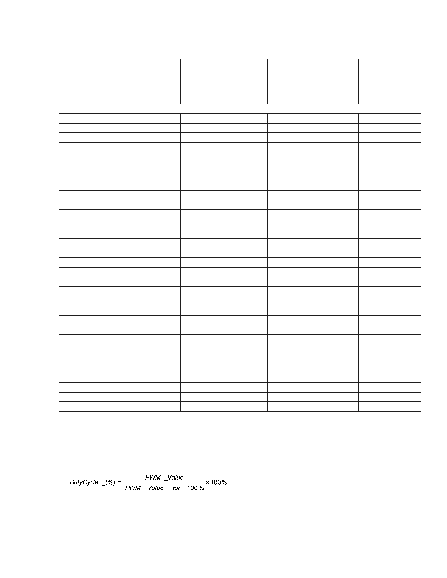
3.0 Application Notes
3.1 FAN CONTROL DUTY CYCLE VS. REGISTER SETTINGS AND FREQUENCY
PWM
Freq
4D
[4:0]
Step
Resolution,
%
PWM
Value
4D [5:0]
for 100%
PWM
Value
4C [5:0] for
about 75%
PWM
Value
4C [5:0]
for 50%
PWM
Freq at
360 kHz
Internal
Clock, kHz
PWM
Freq at
1.4 kHz
Internal
Clock, Hz
Actual Duty
Cycle, % When
75% is Selected
0
Address 0 is mapped to Address 1
1
50
2
1
1
180.0
703.1
50.0
2
25
4
3
2
90.00
351.6
75.0
3
16.7
6
5
3
60.00
234.4
83.3
4
12.5
8
6
4
45.00
175.8
75.0
5
10.0
10
8
5
36.00
140.6
80.0
6
8.33
12
9
6
30.00
117.2
75.0
7
7.14
14
11
7
25.71
100.4
78.6
8
6.25
16
12
8
22.50
87.9
75.0
9
5.56
18
14
9
20.00
78.1
77.8
10
5.00
20
15
10
18.00
70.3
75.0
11
4.54
22
17
11
16.36
63.9
77.27
12
4.16
24
18
12
15.00
58.6
75.00
13
3.85
26
20
13
13.85
54.1
76.92
14
3.57
28
21
14
12.86
50.2
75.00
15
3.33
30
23
15
12.00
46.9
76.67
16
3.13
32
24
16
11.25
43.9
75.00
17
2.94
34
26
17
10.59
41.4
76.47
18
2.78
36
27
18
10.00
39.1
75.00
19
2.63
38
29
19
9.47
37.0
76.32
20
2.50
40
30
20
9.00
35.2
75.00
21
2.38
42
32
21
8.57
33.5
76.19
22
2.27
44
33
22
8.18
32.0
75.00
23
2.17
46
35
23
7.82
30.6
76.09
24
2.08
48
36
24
7.50
29.3
75.00
25
2.00
50
38
25
7.20
28.1
76.00
26
1.92
52
39
26
6.92
27.0
75.00
27
1.85
54
41
27
6.67
26.0
75.93
28
1.79
56
42
28
6.42
25.1
75.00
29
1.72
58
44
29
6.21
24.2
75.86
30
1.67
60
45
30
6.00
23.4
75.00
31
1.61
62
47
31
5.81
22.7
75.81
3.1.1 Computing Duty Cycles for a Given Frequency
Select a PWM Frequency from the first column correspond-
ing to the desired actual frequency in columns 6 or 7. Note
the PWM Value for 100% Duty Cycle.
Find the Duty Cycle by taking the PWM Value of Register 4C
and computing:
Example: For a PWM Frequency of 24, a PWM Value at
100% = 48 and PWM Value actual = 28, then the Duty Cycle
is (28/48) x 100% = 58.3%.
LM63
www.national.com
24
3.0 Application Notes
(Continued)
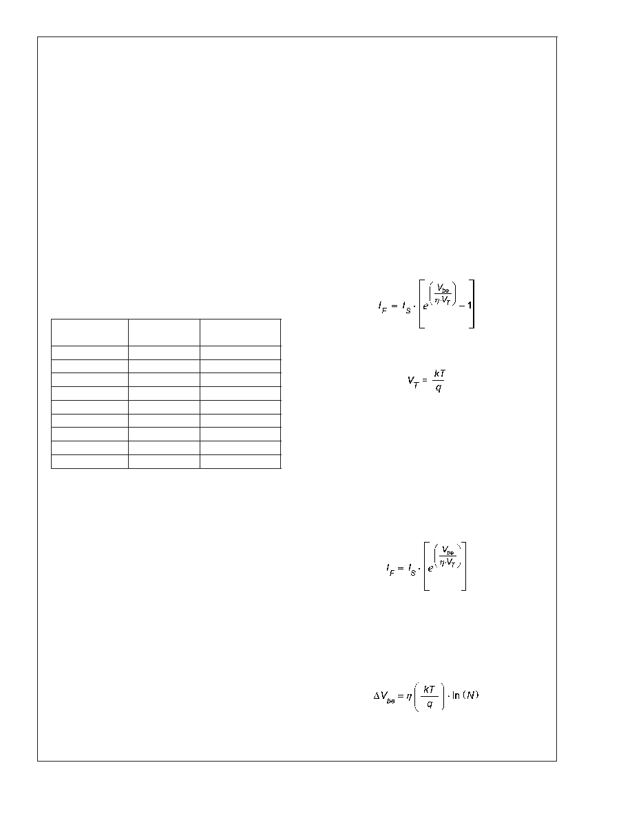
3.2 USE OF THE LOOKUP TABLE FOR NON-LINEAR
PWM VALUES VS TEMPERATURE
The Lookup Table, Registers 50 through 5F, can be used to
create a non-linear PWM vs Temperature curve that could be
used to reduce the acoustic noise from processor fan due to
linear or step transfer functions. An example is given below:
EXAMPLE:
In a particular system it was found that the best acoustic fan
noise performance was found to occur when the PWM vs
Temperature transfer function curve was parabolic in shape.
From 25įC to 105įC the fan is to go from 20% to 100%.
Since there are 8 steps to the Lookup Table we will break up
the Temperature range into 8 separate temperatures. For the
80įC over 8-steps = 10įC per step. This takes care of the
x-axis.
For the PWM Value, we first select the PWM Frequency. In
this example we will make the PWM Frequency (Register
4C) 20.
For 100% Duty Cycle then, the PWM value is 40. For 20%
the minimum is 40 x (0.2) = 8.
We can then arrange the PWM, Temperature pairs in a
parabolic fashion in the form of y = 0.005
∑
(x -25)
2
+ 8
Temperature
PWM Value
Calculated
Closest PWM
Value
25
8.0
8
35
8.5
9
45
10.0
10
55
12.5
13
65
16.0
16
75
20.5
21
85
26.0
26
95
32.5
33
105
40.0
40
We can then program the Lookup Table with the temperature
and Closest PWM Values required for the curve required in
our example.
3.3 NON-IDEALITY FACTOR AND TEMPERATURE
ACCURACY
The LM63 can be applied to remote diode sensing in the
same way as other integrated-circuit temperature sensors. It
can be soldered to a printed-circuit board, and because the
path of best thermal conductivity is between the die and the
pins, its temperature will effectively be that of the printed-
circuit board lands and traces soldered to its pins. This
presumes that the ambient air temperature is nearly the
same as the surface temperature of the printed-circuit board.
If the air temperature is much higher or lower than the
surface temperature, the actual temperature of the LM63 die
will be an intermediate temperature between the surface and
air temperatures. Again, the primary thermal conduction path
is through the leads, so the circuit board surface temperature
will contribute to the die temperature much more than the air
temperature.
To measure the temperature external to the die use a remote
diode. This diode can be located on the die of the target IC,
such as a CPU processor chip, allowing measurement of the
IC's temperature, independent of the LM63's temperature.
The LM63 has been optimized for use with the thermal diode
on the die of an Intel Pentium 4 or a Mobile Pentium 4
Processor-M processor.
A discrete diode can also be used to sense the temperature
of external objects or ambient air. Remember that a discrete
diode's temperature will be affected, and often dominated by,
the temperature of its leads.
Most silicon diodes do not lend themselves well to this
application. It is recommended that a diode-connected
2N3904 transistor be used. The base of the transistor is
connected to the collector and becomes the anode. The
emitter is the cathode.
A LM63 with a diode-connected 2N3904 transistor approxi-
mates the temperature reading of the LM63 with the Pentium
4 processor by 1įC.
T
2N3904
= T
PENTIUM 4
- 1įC
3.3.1 Diode Non_Ideality
When a transistor is connected to a diode the following
relationship holds for V
be
, T, and I
F
:
where
∑
q = 1.6x10
-19
Coulombs (the electron charge)
∑
T = Absolute Temperature in Kelvin
∑
k = 1.38x10
-23
joules/K (Boltzmann's constant)
∑
is the non-ideality factor of the manufacturing process
used to make the thermal diode
∑
I
s
= Saturation Current and is process dependent
∑
I
f
= Forward Current through the base emitter junction
∑
V
be
= Base Emitter Voltage Drop
In the active region, the -1 term is negligible and may be
eliminated, yielding the following equation
In the above equation,
and I
s
are dependent upon the
process that was used in the fabrication of the particular
diode. By forcing two currents with a very controlled ratio (N)
and measuring the resulting voltage difference, it is possible
to eliminate the I
s
term. Solving for the forward voltage
difference yields the relationship:
The voltage seen by the LM63 also includes the I
F
xR
S
voltage drop across the internal series resistance of the
LM63
www.national.com
25
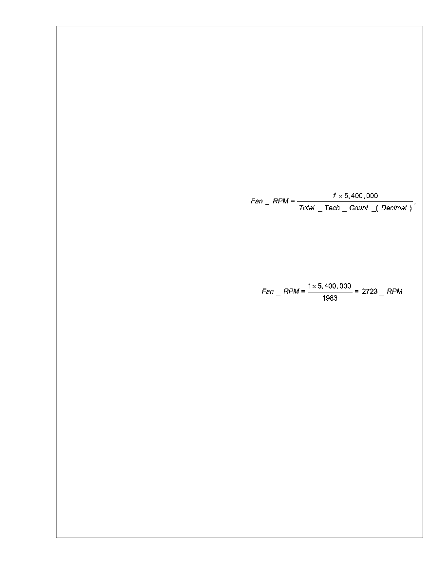
3.0 Application Notes
(Continued)
Pentium 4 processor's thermal diode. The non-ideality factor,
, is the only other parameter not accounted for and de-
pends on the diode that is used for measurement. Since
V
be
is proportional to both
and T, the variations in
cannot be distinguished from variations in temperature.
Since the temperature sensor does not control the non-
ideality factor, it will directly add to the inaccuracy of the
sensor.
For the Intel Pentium 4 and Mobile Pentium 4 Processor-M
processors Intel specifies a
Ī
0.1% variation in
from part to
part. As an example, assume that a temperature sensor has
an accuracy specification of
Ī
1%įC at room temperature of
25įC and process used to manufacture the diode has a
non-ideality variation of
Ī
0.1%. The resulting accuracy will
be:
T
ACC
=
Ī
1įC + (
Ī
0.1% of 298įK) =
Ī
1.3įC
The additional inaccuracy in the temperature measurement
caused by
, can be eliminated if each temperature sensor is
calibrated with the remote diode that it will be paired with-
.Refer to the processor datasheet for the non-ideality factor.
3.3.2 Compensating for Diode Non-Ideality
In order to compensate for the errors introduced by non-
ideality, the temperature sensor is calibrated for a particular
processor. National Semiconductor temperature sensors are
always calibrated to the typical non-ideality of a particular
processor type.
The LM63 is calibrated for the non-ideality of the 0.13 micron
Intel Pentium 4 and Mobile Pentium 4 Processor-M proces-
sors.
When a temperature sensor, calibrated for a specific type of
processor is used with a different processor type or a given
processor type has a non-ideality that strays form the typical
value, errors are introduced.
Temperature errors associated with non-ideality may be in-
troduced in a specific temperature range of concern through
the use of the Temperature Offset Registers 11
HEX
and
12
HEX
.
The
user
is
encouraged
to
send
an
e-mail
to
hardware.monitor.team
@
nsc.com to further request infor-
mation on our recommended setting of the offset register for
different processor types.
3.4 COMPUTING RPM OF THE FAN FROM THE TACH
COUNT
The Tach Count Registers 46
HEX
and 47
HEX
count the num-
ber of periods of the 90 kHz tachometer clock in the LM63 for
the tachometer input from the fan assuming a 2 pulse per
revolution fan tachometer, such as the fans supplied with the
Pentium 4 boxed processors. The RPM of the fan can be
computed from the Tach Count Registers 46
HEX
and 47
HEX
.
This can best be shown through an example.
Example:
Given: the fan used has a tachometer output with 2 per
revolution.
Let:
Register 46 (LSB) is BF
HEX
= Decimal (11 x 16) + 15 = 191
and
Register 47 (MSB) is 7
HEX
= Decimal (7 x 256) = 1792.
The total Tach Count, in decimal, is 191 + 1792 = 1983.
The RPM is computed using the formula
where
f = 1 for 2 pulses/rev fan tachometer output;
f = 2 for 1 pulse/rev fan tachometer output, and
f = 2 / 3 for 3 pulses/rev fan tachometer output
For our example
LM63
www.national.com
26
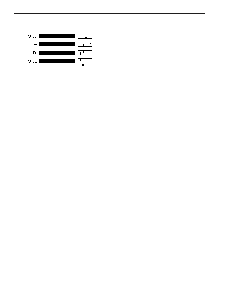
3.0 Application Notes
(Continued)
3.5 PCB LAYOUT FOR MINIMIZING NOISE
In a noisy environment, such as a processor mother board,
layout considerations are very critical. Noise induced on
traces running between the remote temperature diode sen-
sor and the LM63 can cause temperature conversion errors.
Keep in mind that the signal level the LM63 is trying to
measure is in microvolts. The following guidelines should be
followed:
1.
Place a 0.1 ĶF power supply bypass capacitor as close
as possible to the V
DD
pin and the recommended 2.2 nF
capacitor as close as possible to the LM63's D+ and D-
pins. Make sure the traces to the 2.2 nF capacitor are
matched.
2.
Ideally, the LM63 should be placed within 10 cm of the
Processor diode pins with the traces being as straight,
short and identical as possible. Trace resistance of 1
can cause as much as 1įC of error. This error can be
compensated by using the Remote Temperature Offset
Registers, since the value placed in these registers will
automatically be subtracted from or added to the remote
temperature reading.
3.
Diode traces should be surrounded by a GND guard ring
to either side, above and below if possible. This GND
guard should not be between the D+ and D- lines. In the
event that noise does couple to the diode lines it would
be ideal if it is coupled common mode. That is equally to
the D+ and D- lines.
4.
Avoid routing diode traces in close proximity to power
supply switching or filtering inductors.
5.
Avoid running diode traces close to or parallel to high
speed digital and bus lines. Diode traces should be kept
at least 2 cm apart from the high speed digital traces.
6.
If it is necessary to cross high speed digital traces, the
diode traces and the high speed digital traces should
cross at a 90 degree angle.
7.
The ideal place to connect the LM63's GND pin is as
close as possible to the Processor's GND associated
with the sense diode.
8.
Leakage current between D+ and GND should be kept
to a minimum. One nano-ampere of leakage can cause
as much as 1įC of error in the diode temperature read-
ing. Keeping the printed circuit board as clean as pos-
sible will minimize leakage current.
Noise coupling into the digital lines greater than 400 mVp-p
(typical hysteresis) and undershoot less than 500 mV below
GND, may prevent successful SMBus communication with
the LM63. SMBus no acknowledge is the most common
symptom, causing unnecessary traffic on the bus. Although
the SMBus maximum frequency of communication is rather
low (100 kHz max), care still needs to be taken to ensure
proper termination within a system with multiple parts on the
bus and long printed circuit board traces. An RC lowpass
filter with a 3 dB corner frequency of about 40 MHz is
included on the LM63's SMBCLK input. Additional resistance
can be added in series with the SMBData and SMBCLK lines
to further help filter noise and ringing. Minimize noise cou-
pling by keeping digital traces out of switching power supply
areas as well as ensuring that digital lines containing high
speed data communications cross at right angles to the
SMBData and SMBCLK lines.
20057021
FIGURE 10. Ideal Diode Trace Layout
LM63
www.national.com
27
Physical Dimensions
inches (millimeters) unless otherwise noted
8-Lead (0.154-Inch Wide) Molded Narrow Small-Outline Package (SOIC)
JEDEC Registration Number MS-012
Order Number LM63CIM
NS Package Number M008A
LIFE SUPPORT POLICY
NATIONAL'S PRODUCTS ARE NOT AUTHORIZED FOR USE AS CRITICAL COMPONENTS IN LIFE SUPPORT
DEVICES OR SYSTEMS WITHOUT THE EXPRESS WRITTEN APPROVAL OF THE PRESIDENT AND GENERAL
COUNSEL OF NATIONAL SEMICONDUCTOR CORPORATION. As used herein:
1. Life support devices or systems are devices or
systems which, (a) are intended for surgical implant
into the body, or (b) support or sustain life, and
whose failure to perform when properly used in
accordance with instructions for use provided in the
labeling, can be reasonably expected to result in a
significant injury to the user.
2. A critical component is any component of a life
support device or system whose failure to perform
can be reasonably expected to cause the failure of
the life support device or system, or to affect its
safety or effectiveness.
National Semiconductor
Americas Customer
Support Center
Email: new.feedback@nsc.com
Tel: 1-800-272-9959
National Semiconductor
Europe Customer Support Center
Fax: +49 (0) 180-530 85 86
Email: europe.support@nsc.com
Deutsch Tel: +49 (0) 69 9508 6208
English
Tel: +44 (0) 870 24 0 2171
FranÁais Tel: +33 (0) 1 41 91 8790
National Semiconductor
Asia Pacific Customer
Support Center
Email: ap.support@nsc.com
National Semiconductor
Japan Customer Support Center
Fax: 81-3-5639-7507
Email: jpn.feedback@nsc.com
Tel: 81-3-5639-7560
www.national.com
LM63
Ī
1įC/
Ī
3įC
Accurate
Remote
Diode
Digital
T
emperature
Sensor
with
Integrated
Fan
Control
National does not assume any responsibility for use of any circuitry described, no circuit patent licenses are implied and National reserves the right at any time without notice to change said circuitry and specifications.