 | –≠–ª–µ–∫—Ç—Ä–æ–Ω–Ω—ã–π –∫–æ–º–ø–æ–Ω–µ–Ω—Ç: LM66 | –°–∫–∞—á–∞—Ç—å:  PDF PDF  ZIP ZIP |
LM66
Dual Output Internally Preset Thermostat
General Description
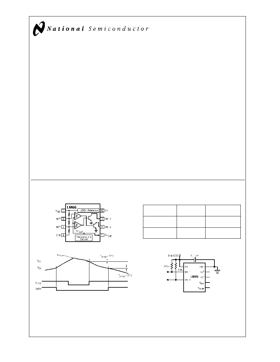
The LM66 is a precision low power thermostat. Two stable
temperature trip points (V
T1
and V
T2
) are generated by divid-
ing down the LM66 1.250V bandgap voltage reference using
a resistors divider network. The LM66 has two digital out-
puts. OUT1 goes LOW when the temperature exceeds T1
and goes HIGH when the the temperature goes below
(T1≠T
HYST
). Similarly, OUT2 goes LOW when the tempera-
ture exceeds T2 and goes HIGH when the temperature goes
below (T2≠T
HYST
). T
HYST
is an internally set 5∞C typical hys-
teresis.
The LM66 is currently available in an 8-lead small outline
package.
Applications
n
Microprocessor Thermal Management
n
Appliances
n
Portable Battery Powered 3.0V or 5V Systems
n
Fan Control
n
Industrial Process Control
n
HVAC Systems
n
Remote Temperature Sensing
n
Electronic System Protection
Features
n
Digital outputs support TTL logic levels
n
Internal temperature sensor
n
2 internal comparators with hysteresis
n
Internal voltage reference
n
Currently available in 8-pin SO plastic package
Key Specifications
n
Power Supply Voltage
2.7V to 10V
n
Power Supply Current
250 µA (max)
n
V
REF
1.250V
±
1.4% (max)
n
Hysteresis Temperature
5∞C
n
Internal Temperature Sensor
Output Voltage
(+6.20 mV/∞C x T) +400 mV
n
Temperature Trip Point Accuracy
±
3∞C (max)
n
T1 set point
+73∞C
n
T2 set point
+82∞C
Simplified Block Diagram and
Connection Diagram
Ordering Information
TABLE 1.
Order Number
LM66CIM-
RLSKB
LM66CIMX-
RLSKB
NS Tackage
Number
M08A
M08A
Transport Media
Bulk Rail
2500 Units Tape
& Reel
Typical Application
DS100854-1
DS100854-2
DS100854-3
April 2000
LM66
Dual
Output
Internally
Preset
Thermostat
© 2000 National Semiconductor Corporation
DS100854
www.national.com
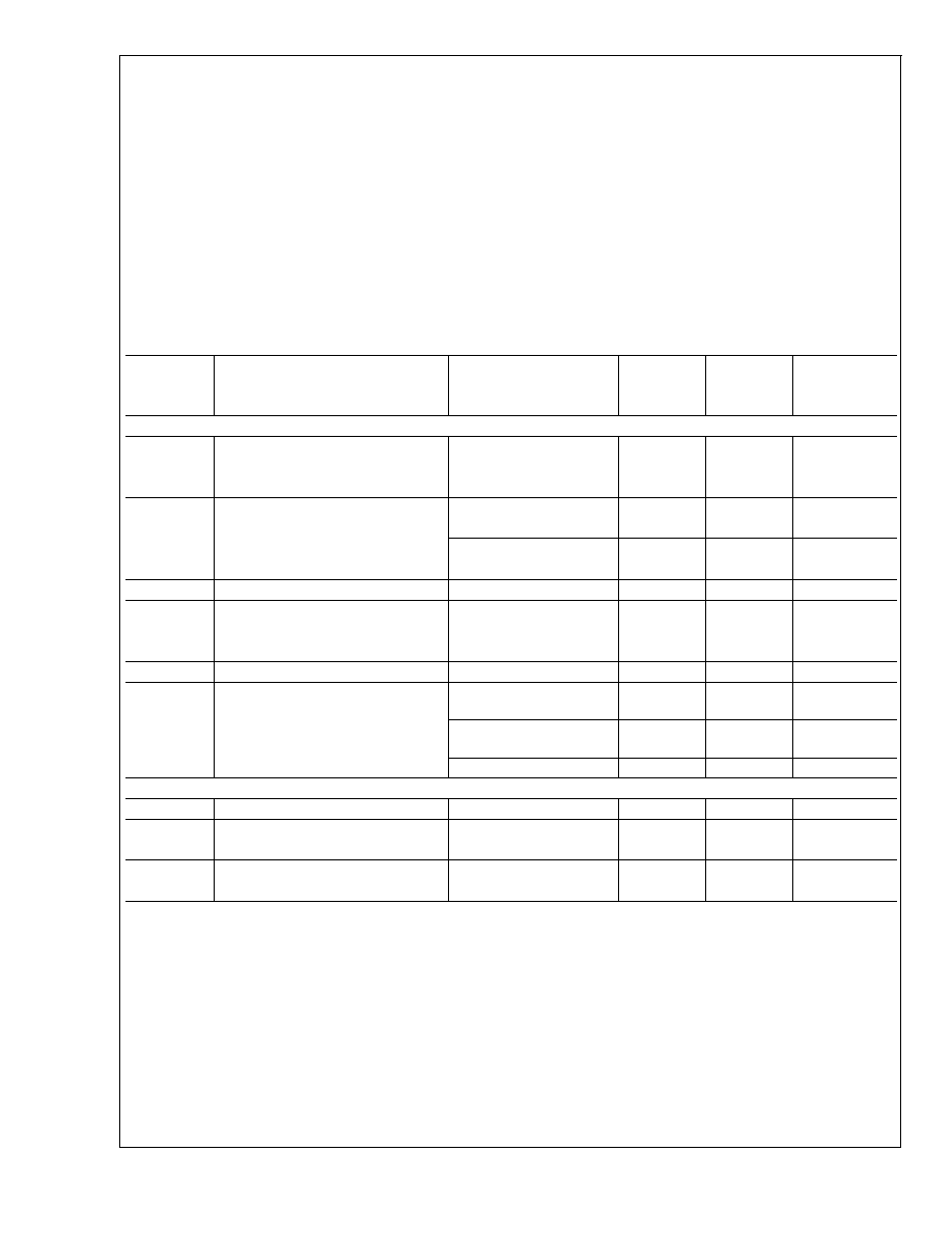
Absolute Maximum Ratings
(Note 1)
Input Voltage
12V
Input Current at any pin (Note 2)
5 mA
Package Input Current (Note 2)
20 mA
Package Dissipation at T
A
= 25∞C
(Note 3)
900 mW
ESD Susceptibility (Note 4)
Human Body Model
1000V
Machine Model
200V
Soldering Information
SO Package (Note 5) :
Vapor Phase (60 seconds)
215∞C
Infrared (15 seconds)
220∞C
Storage Temperature
-65∞C to + 150∞C
Operating Ratings
(Note 1)
Operating Temperature Range
T
MIN
T
A
T
MAX
LM66CIM
-40∞C
T
A
+125∞C
Positive Supply Voltage (V
+
)
+2.7V to +10V
Maximum V
OUT1
and V
OUT2
+10V
LM66 Electrical Characteristics
The following specifications apply for V
+
= 2.7 V
DC
, and V
REF
load current = 0 µA unless otherwise specified. Boldface lim-
its apply for T
A
= T
J
= T
MIN
to T
MAX
; all other limits T
A
= T
J
= 25∞C unless otherwise specified.
Typical
LM66CIM
Units
Symbol
Parameter
Conditions
(Note 6)
Limits
(Limits)
(Note 7)
Temperature Sensor
Trip Point Accuracy (Includes
V
REF
, Comparator Offset, and
+25∞C
T
A
+85∞C
±
3
∞C (max)
Temperature Sensitivity errors)
Trip Point Hysteresis
T
A
= +73∞C
6
4.5
∞C (min)
7.5
∞C (max)
T
A
= +82∞C
6
4.5
∞C (min)
7.5
∞C (max)
Internal Temperature Sensitivity
+6.20
mV/∞C
Temperature Sensitivity Error
+25∞C
T
A
+85∞C
±
3
∞C (max)
-25∞C
T
A
+125∞C
±
4
∞C (max)
-40∞C
T
A
-25∞C
±
5
∞C (max)
Output Impedance
-1 µA
I
L
+40 µA
1500
(max)
Line Regulation
+3.0V
V
+
+10V,
+25∞C
T
A
+85∞C
±
0.36
mV/V (max)
+3.0V
V
+
+10V,
-40∞C
T
A
<
25∞C
±
0.61
mV/V (max)
+2.7V
V
+
+3.3V
±
2.3
mV (max)
V
REF
Output
V
REF
V
REF
Nominal
1.250V
V
V
REF
Error
±
1.4
% (max)
±
17.5
mV (max)
V
REF
/
V
+
Line Regulation
+3.0V
V
+
+10V
0.13
0.21
mV/V (max)
+2.7V
V
+
+3.3V
0.15
1.5
mV (max)
LM66
www.national.com
2
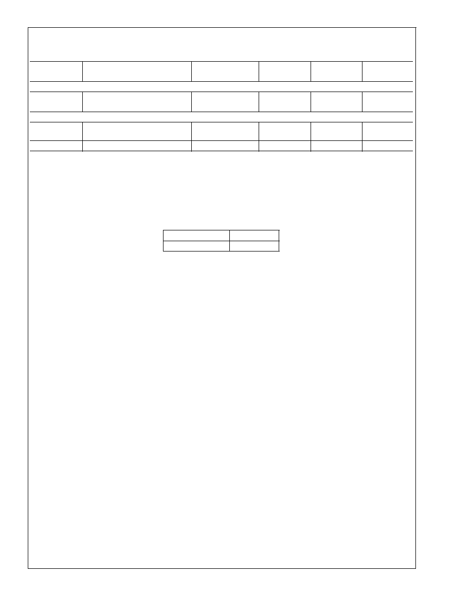
LM66 Electrical Characteristics
The following specifications apply for V
+
= 2.7 V
DC
, and V
REF
load current = 50 µA unless otherwise specified. Boldface lim-
its apply for T
A
= T
J
= T
MIN
to T
MAX
; all other limits T
A
= T
J
= 25∞C unless otherwise specified.
Symbol
Parameter
Conditions
Typical
Limits
Units
(Note 6)
(Note 7)
(Limits)
V
+
Power Supply
I
S
Supply Current
V
+
= +10V
250
µA (max)
V
+
= +2.7V
250
µA (max)
Digital Output(s)
I
OUT("1")
Logical "1" Output Leakage
Current
V
+
= +5.0V
1
µA (max)
V
OUT("0")
Logical "0" Output Voltage
I
OUT
= +50 µA
0.4
V (max)
Note 1: Absolute Maximum Ratings indicate limits beyond which damage to the device may occur. Operating Ratings indicate conditions for which the device is func-
tional, but do not guarantee specific performance limits. For guaranteed specifications and test conditions, see the Electrical Characteristics. The guaranteed speci-
fications apply only for the test conditions listed. Some performance characteristics may degrade when the device is not operated under the listed test conditions.
Note 2: When the input voltage (V
I
) at any pin exceeds the power supply (V
I
<
GND or V
I
>
V
+
), the current at that pin should be limited to 5 mA. The 20 mA maxi-
mum package input current rating limits the number of pins that can safely exceed the power supplies with an input current of 5 mA to four.
Note 3: The maximum power dissipation must be derated at elevated temperatures and is dictated by T
Jmax
(maximum junction temperature),
JA
(junction to am-
bient thermal resistance) and T
A
(ambient temperature). The maximum allowable power dissipation at any temperature is P
D
= (T
Jmax
≠T
A
)/
JA
or the number given
in the Absolute Maximum Ratings, whichever is lower. For this device, T
Jmax
= 125∞C. For this device the typical thermal resistance (
JA
) of the different package
types when board mounted follow:
Package Type
JA
M08A
110∞C/W
Note 4: The human body model is a 100 pF capacitor discharge through a 1.5 k
resistor into each pin. The machine model is a 200 pF capacitor discharged directly
into each pin.
Note 5: See AN450 "Surface Mounting Methods and Their Effects on Product Reliability" or the section titled "Surface Mount" found in any post 1986 National Semi-
conductor Linear Data Book for other methods of soldering surface mount devices.
Note 6: Typicals are at T
J
= T
A
= 25∞C and represent most likely parametric norm.
Note 7: Limits are guaranteed to National's AOQL (Average Outgoing Quality Level).
LM66
www.national.com
3
Part Number Template
The series of digits labled vw xy z in the part number LM66CIM-vw xy z, describe the
set points and the function of OUT1 and OUT2 as follows:
The place holders v w describe the set point of T1 as shown in the following table.
The place holders xy describe the set point of T2 as shown in the following table. z=0 (Other assignments are reserved.)
For example the part number LM66CIM-RLSKB has: T1 = 73∞C, T2 = 82∞C, OUT1 and OUT2 set as active-low
open-collector outputs with OUT1 mapped to pin 7 and OUT2 mapped to pin 6.
v, w, x and y
Temperature (∞C)
B
-5
C
-4
D
-3
F
-2
G
-1
H
-0
J
1
K
2
L
3
N
4
v, w, x and y
Temperature (∞C)
P
5
Q
6
R
7
S
8
T
9
V
10
X
11
Y
12
Z
13
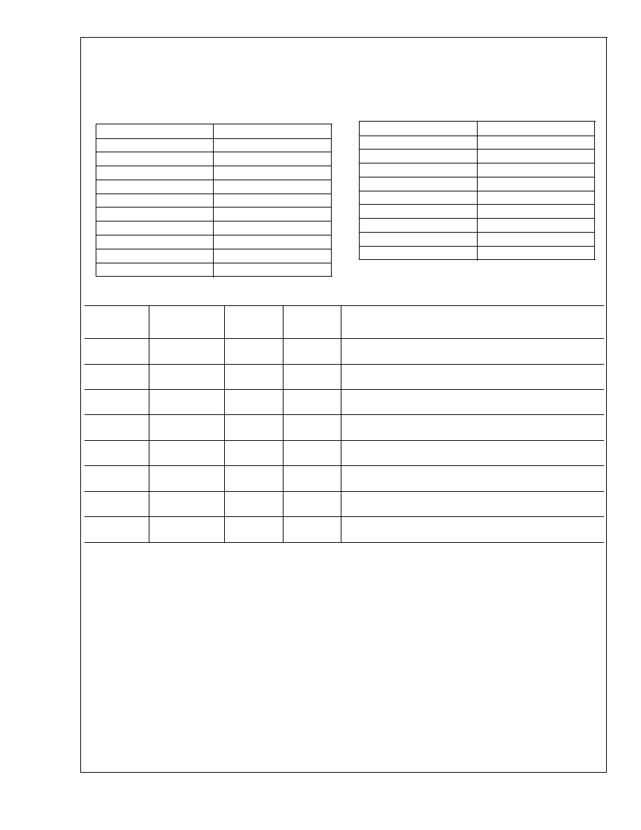
The value of z describes the assignment/function of OUT1 and OUT2 as shown in the following table:
Active
Low//High
Open
Collector/
Totem Pole
Mapping
Value of z
Function of OUT1 and OUT2
0
0
0
B
Active-Low, Open-Collector, OUT1 mapped to pin 7, OUT2
mapped to pin 6
0
0
1
C
Active-Low, Open-Collector, OUT1 mapped to pin 6, OUT2
mapped to pin 7
0
1
0
D
Active-Low, Totem Pole, OUT1 mapped to pin 7, OUT2
mapped to pin 6
0
1
1
F
Active-Low, Totem Pole, OUT1 mapped to pin 6, OUT2
mapped to pin 7
1
0
0
G
Active-High, Open-Collector, OUT1 mapped to pin 7, OUT2
mapped to pin 6
1
0
1
H
Active-High, Open-Collector, OUT1 mapped to pin 6, OUT2
mapped to pin 7
1
1
0
J
Active-High, Totem Pole, OUT1 mapped to pin 7, OUT2
mapped to pin 6
1
1
1
K
Active-High, Totem Pole, OUT1 mapped to pin 6, OUT2
mapped to pin 7
LM66
www.national.com
4
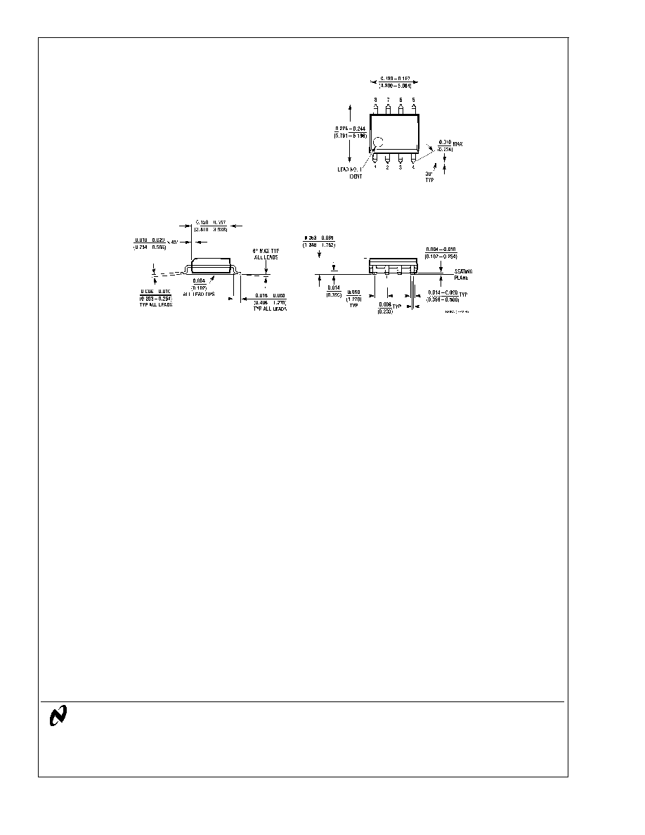
Physical Dimensions
inches (millimeters) unless otherwise noted
LIFE SUPPORT POLICY
NATIONAL'S PRODUCTS ARE NOT AUTHORIZED FOR USE AS CRITICAL COMPONENTS IN LIFE SUPPORT
DEVICES OR SYSTEMS WITHOUT THE EXPRESS WRITTEN APPROVAL OF THE PRESIDENT AND GENERAL
COUNSEL OF NATIONAL SEMICONDUCTOR CORPORATION. As used herein:
1. Life support devices or systems are devices or
systems which, (a) are intended for surgical implant
into the body, or (b) support or sustain life, and
whose failure to perform when properly used in
accordance with instructions for use provided in the
labeling, can be reasonably expected to result in a
significant injury to the user.
2. A critical component is any component of a life
support device or system whose failure to perform
can be reasonably expected to cause the failure of
the life support device or system, or to affect its
safety or effectiveness.
National Semiconductor
Corporation
Americas
Tel: 1-800-272-9959
Fax: 1-800-737-7018
Email: support@nsc.com
National Semiconductor
Europe
Fax: +49 (0) 180-530 85 86
Email: europe.support@nsc.com
Deutsch Tel: +49 (0) 69 9508 6208
English
Tel: +44 (0) 870 24 0 2171
FranÁais Tel: +33 (0) 1 41 91 8790
National Semiconductor
Asia Pacific Customer
Response Group
Tel: 65-2544466
Fax: 65-2504466
Email: ap.support@nsc.com
National Semiconductor
Japan Ltd.
Tel: 81-3-5639-7560
Fax: 81-3-5639-7507
www.national.com
8-Lead (0.150" Wide) Molded Small Outline Package, JEDEC
Order Number LM66CIM or LM66CIMX
NS Package Number M08A
LM66
Dual
Output
Internally
Preset
Thermostat
National does not assume any responsibility for use of any circuitry described, no circuit patent licenses are implied and National reserves the right at any time without notice to change said circuitry and specifications.