LM725
Operational Amplifier
General Description
The LM725/LM725A/LM725C are operational amplifiers fea-
turing superior performance in applications where low noise,
low drift, and accurate closed-loop gain are required. With
high common mode rejection and offset null capability, it is
especially suited for low level instrumentation applications
over a wide supply voltage range.
The LM725A has tightened electrical performance with
higher input accuracy and like the LM725, is guaranteed
over a -55∞C to +125∞C temperature range. The LM725C
has slightly relaxed specifications and has its performance
guaranteed over a 0∞C to 70∞C temperature range.
Features
n
High open loop gain
3,000,000
n
Low input voltage drift
0.6 µV/∞C
n
High common mode rejection
120 dB
n
Low input noise current
0.15 pA/
Hz
n
Low input offset current
2 nA
n
High input voltage range
±
14V
n
Wide power supply range
±
3V to
±
22V
n
Offset null capability
n
Output short circuit protection
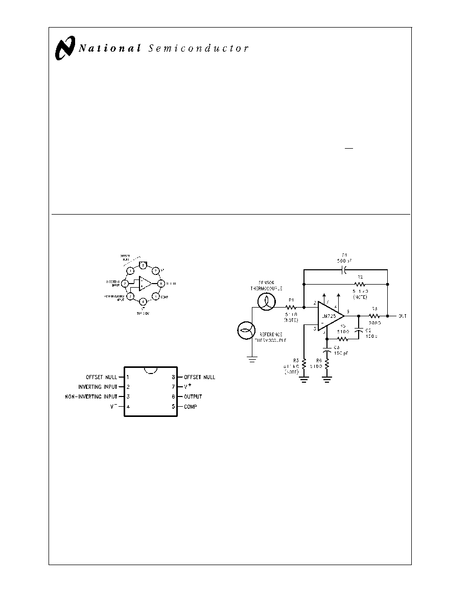
Connection Diagram
Typical Applications
Metal Can Package
DS010474-1
Order Number LM725H/883, LM725CH or LM725AH/883
See NS Package Number H08C
Dual-In-Line Package
DS010474-2
Order Number LM725CN
See NS Package Number N08E
Thermocouple Amplifier
DS010474-10
August 2000
LM725
Operational
Amplifier
© 2000 National Semiconductor Corporation
DS010474
www.national.com
Absolute Maximum Ratings
(Note 1)
If Military/Aerospace specified devices are required,
please contact the National Semiconductor Sales Office/
Distributors for availability and specifications.
Supply Voltage
±
22V
Internal Power Dissipation (Note 2)
500 mW
Differential Input Voltage
±
5V
Input Voltage (Note 3)
±
22V
Storage Temperature Range
-65∞C to +150∞C
Lead Temperature
(Soldering, 10 Sec.)
260∞C
Maximum Junction Temperature
150∞C
Operating Temperature Range
T
A(MIN)
T
A(MAX)
LM725
-55∞C
to
+125∞C
LM725A
-55∞C
to
+125∞C
LM725C
0∞C
to
+70∞C
Electrical Characteristics
(Note 4)
Parameter
Conditions
LM725A
LM725
LM725C
Units
Min
Typ
Max
Min
Typ
Max
Min
Typ
Max
Input Offset Voltage
T
A
= 25∞C,
0.5
0.5
1.0
0.5
2.5
mV
(Without External Trim)
R
S
10 k
Input Offset Current
T
A
= 25∞C
2.0
5.0
2.0
20
2.0
35
nA
Input Bias Current
T
A
= 25∞C
42
80
42
100
42
125
nA
Input Noise Voltage
T
A
= 25∞C
f
o
= 10 Hz
15
15
15
nV/
Hz
f
o
= 100 Hz
9.0
9.0
9.0
nV/
Hz
f
o
= 1 kHz
8.0
8.0
8.0
nV/
Hz
Input Noise Current
T
A
= 25∞C
f
o
= 10 Hz
1.0
1.0
1.0
pA/
Hz
f
o
= 100 Hz
0.3
0.3
0.3
pA/
Hz
f
o
= 1 kHz
0.15
0.15
0.15
pA/
Hz
Input Resistance
T
A
= 25∞C
1.5
1.5
1.5
M
Input Voltage Range
T
A
= 25∞C
±
13.5
±
14
±
13.5
±
14
±
13.5
±
14
V
Large Signal Voltage
Gain
T
A
= 25∞C,
R
L
2 k
,
1000
3000
1000
3000
250
3000
V/mV
V
OUT
=
±
10V
Common-Mode
T
A
= 25∞C,
120
110
120
94
120
dB
Rejection Ratio
R
S
10 k
Power Supply
T
A
= 25∞C,
2.0
5.0
2.0
10
2.0
35
µV/V
Rejection Ratio
R
S
10 k
Output Voltage Swing
T
A
= 25∞C,
R
L
10 k
±
12.5
±
13.5
±
12
±
13.5
±
12
±
13.5
V
R
L
2 k
±
12.0
±
13.5
±
10
±
13.5
±
10
±
13.5
V
Power Consumption
T
A
= 25∞C
80
105
80
105
80
150
mW
Input Offset Voltage
R
S
10 k
0.7
1.5
3.5
mV
(Without External Trim)
Average Input Offset
R
S
= 50
Voltage Drift
2.0
2.0
5.0
2.0
µV/∞C
(Without External Trim)
Average Input Offset
R
S
= 50
Voltage Drift
0.6
1.0
0.6
0.6
µV/∞C
(With External Trim)
Input Offset Current
T
A
= T
MAX
1.2
4.0
1.2
20
1.2
35
nA
T
A
= T
MIN
7.5
18.0
7.5
40
4.0
50
nA
Average Input Offset
35
90
35
150
10
pA/∞C
Current Drift
Input Bias Current
T
A
= T
MAX
20
70
20
100
125
nA
T
A
= T
MIN
80
180
80
200
250
nA
LM725
www.national.com
2
Electrical Characteristics
(Note 4) (Continued)
Parameter
Conditions
LM725A
LM725
LM725C
Units
Min
Typ
Max
Min
Typ
Max
Min
Typ
Max
Large Signal Voltage
Gain
R
L
2 k
T
A
= T
MAX
1,000,000
1,000,000
125,000
V/V
R
L
2 k
T
A
= T
MIN
500,000
250,000
125,000
V/V
Common-Mode
R
S
10 k
110
100
115
dB
Rejection Ratio
Power Supply
R
S
10 k
8.0
20
20
µV/V
Rejection Ratio
Output Voltage Swing
R
L
2 k
±
12
±
10
±
10
V
Note 1: "Absolute Maximum Ratings" indicate limits beyond which damage to the device may occur. Operating Ratings indicate conditions for which the device is
functional, but do not guarantee specific performance limits.
Note 2: Derate at 150∞C/W for operation at ambient temperatures above 75∞C.
Note 3: For supply voltages less than
±
22V, the absolute maximum input voltage is equal to the supply voltage.
Note 4: These specifications apply for V
S
=
±
15V unless otherwise specified.
Note 5: For Military electrical specifications RETS725AX are available for LM725AH and RETS725X are available for LM725H.
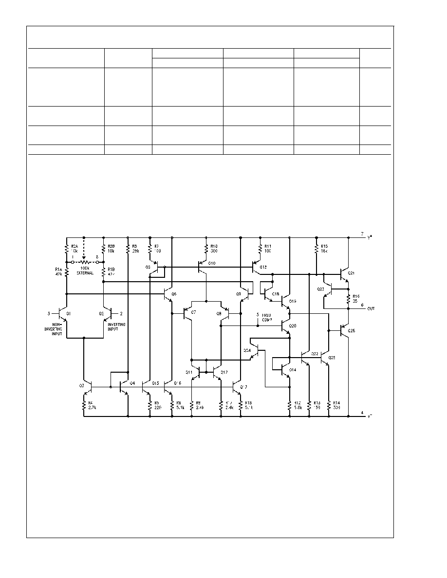
Schematic Diagram
DS010474-5
LM725
www.national.com
3
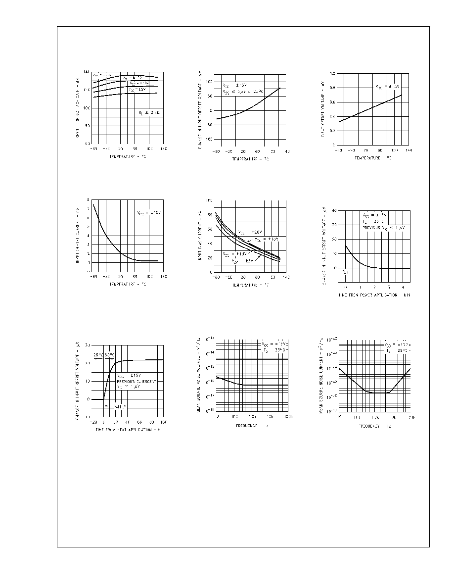
Typical Performance Characteristics
Voltage Gain vs Temperature
for Supply Voltages
DS010474-15
Change in Trimmed Input
Offset Voltage vs Temperature
DS010474-16
Untrimmed Input Offset
Voltage vs Temperature
DS010474-17
Input Offset Current
vs Temperature
DS010474-18
Input Bias Current
vs Temperature
DS010474-19
Stabilization Time of
Input Offset Voltage
from Power Turn-On
DS010474-20
Change in Input
Offset Voltage Due to
Thermal Shock vs Time
DS010474-21
Input Noise
Voltage vs Frequency
DS010474-22
Input Noise
Current vs Frequency
DS010474-23
LM725
www.national.com
4
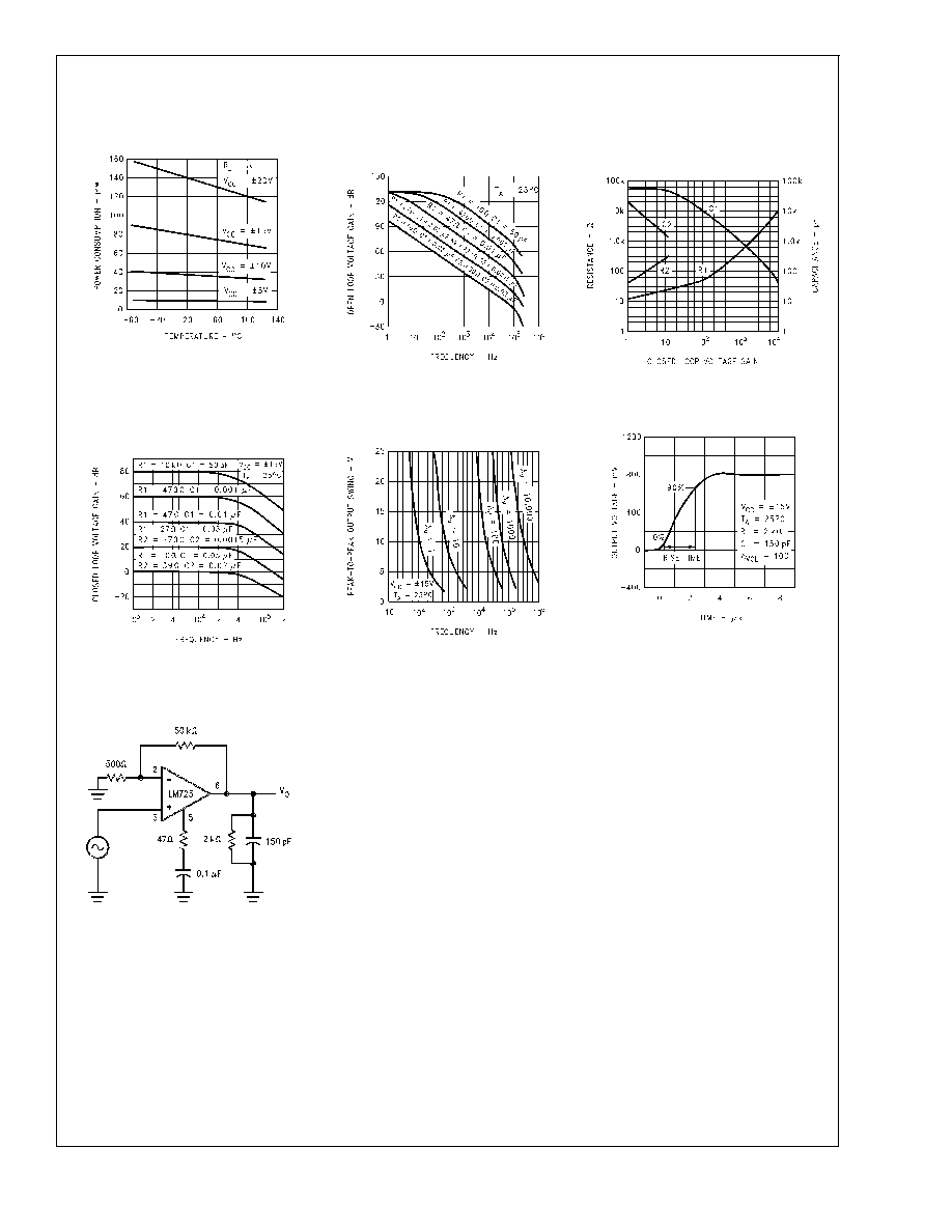
Typical Performance Characteristics
(Continued)
Note 6: Performance is shown using recommended compensation networks.
Power Consumption
vs Temperature
DS010474-24
Open Loop Frequency
Response for Values
of Compensation (Note 6)
DS010474-25
Values for Suggested Compen-
sation Networks vs Various
Close Loop Voltage Gains
DS010474-26
Frequency Response for
Various Close Loop
Gain (Note 6)
DS010474-27
Output Voltage Swing
vs Frequency (Note 6)
DS010474-28
Transient Response
DS010474-29
Transient Response Test Circuit
DS010474-8
LM725
www.national.com
5
Auxiliary Circuits
Compensation Component Values
A
V
R
1
C
1
R
2
C
2
(
)
(µF)
(
)
(µF)
10,000
10k
50 pF
1,000
470
0.001
100
47
0.01
10
27
0.05
270
0.0015
1
10
0.05
39
0.02
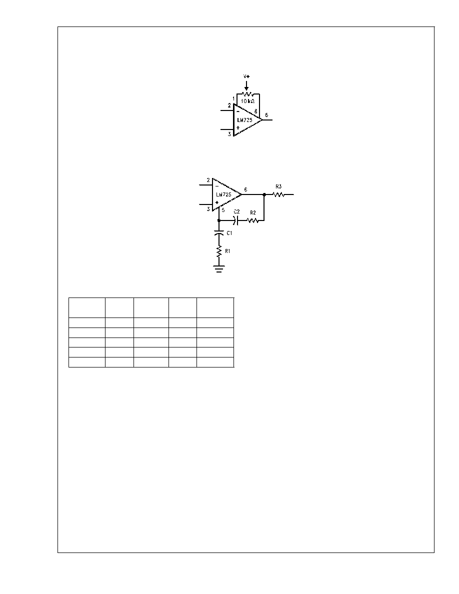
Voltage Offset
Null Circuit
DS010474-3
Frequency Compensation
Circuit
DS010474-4
LM725
www.national.com
6
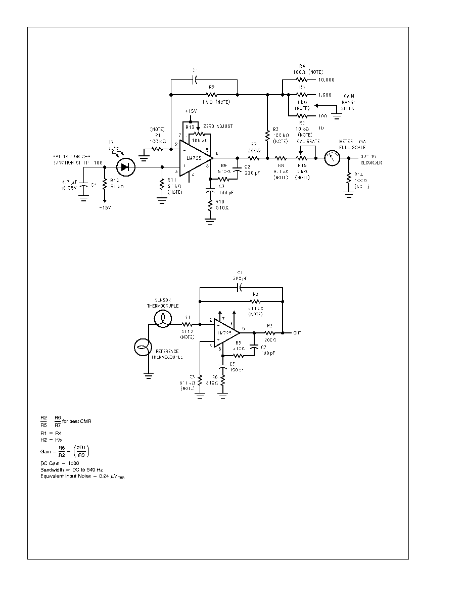
Typical Applications
Photodiode Amplifier
DS010474-9
DC Gains = 10,000; 1,000; 100; and 10
Bandwidth = Determined by value of C1
Thermocouple Amplifier
DS010474-10
Note: Indicates
±
1% metal film resistors recommended for temperature stability.
LM725
www.national.com
7
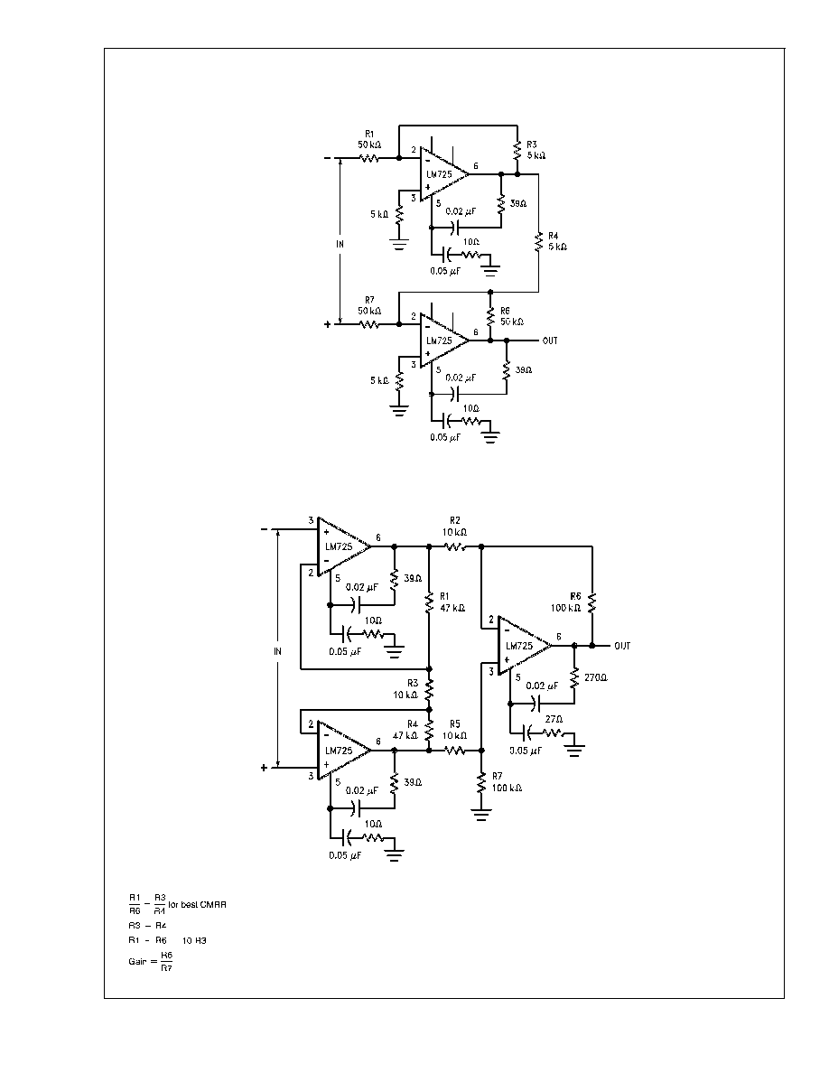
Typical Applications
(Continued)
±
100V Common Mode Range Differential Amplifier
DS010474-11
Instrumentation Amplifier with High
Common Mode Rejection
DS010474-12
LM725
www.national.com
8

Typical Applications
(Continued)
Precision Amplifier A
VCL
= 1000
DS010474-13
LM725
www.national.com
9
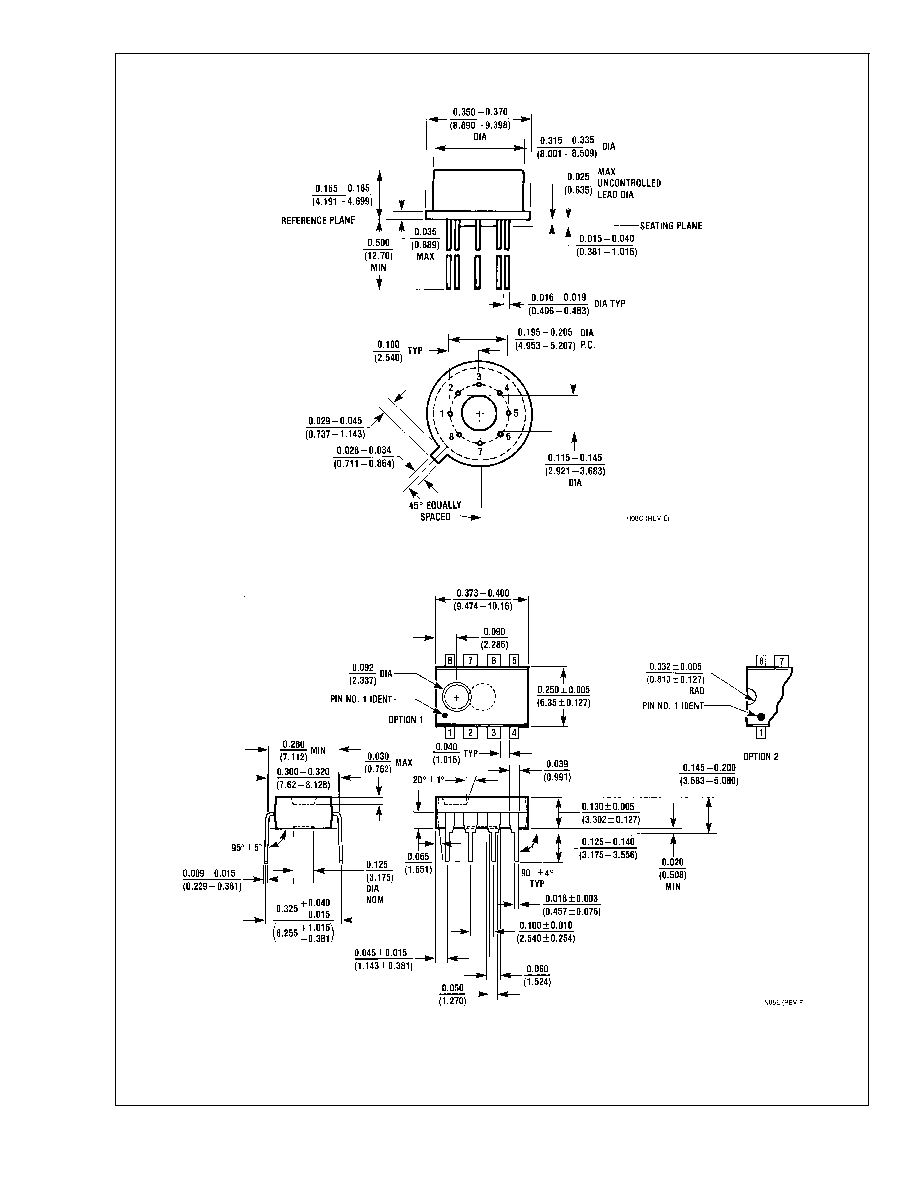
Physical Dimensions
inches (millimeters) unless otherwise noted
Order Number LM725H/883, LM725CH or LM725AH/883
NS Package Number H08C
Order Number LM725CN
NS Package Number N08E
LM725
www.national.com
10

Notes
LIFE SUPPORT POLICY
NATIONAL'S PRODUCTS ARE NOT AUTHORIZED FOR USE AS CRITICAL COMPONENTS IN LIFE SUPPORT
DEVICES OR SYSTEMS WITHOUT THE EXPRESS WRITTEN APPROVAL OF THE PRESIDENT AND GENERAL
COUNSEL OF NATIONAL SEMICONDUCTOR CORPORATION. As used herein:
1. Life support devices or systems are devices or
systems which, (a) are intended for surgical implant
into the body, or (b) support or sustain life, and
whose failure to perform when properly used in
accordance with instructions for use provided in the
labeling, can be reasonably expected to result in a
significant injury to the user.
2. A critical component is any component of a life
support device or system whose failure to perform
can be reasonably expected to cause the failure of
the life support device or system, or to affect its
safety or effectiveness.
National Semiconductor
Corporation
Americas
Tel: 1-800-272-9959
Fax: 1-800-737-7018
Email: support@nsc.com
National Semiconductor
Europe
Fax: +49 (0) 180-530 85 86
Email: europe.support@nsc.com
Deutsch Tel: +49 (0) 69 9508 6208
English
Tel: +44 (0) 870 24 0 2171
FranÁais Tel: +33 (0) 1 41 91 87 90
National Semiconductor
Asia Pacific Customer
Response Group
Tel: 65-2544466
Fax: 65-2504466
Email: ap.support@nsc.com
National Semiconductor
Japan Ltd.
Tel: 81-3-5639-7560
Email: nsj.crc@jksmtp.nsc.com
Fax: 81-3-5639-7507
www.national.com
LM725
Operational
Amplifier
National does not assume any responsibility for use of any circuitry described, no circuit patent licenses are implied and National reserves the right at any time without notice to change said circuitry and specifications.