LM74
SPI/MICROWIRE
TM
12-Bit Plus Sign Temperature Sensor
General Description
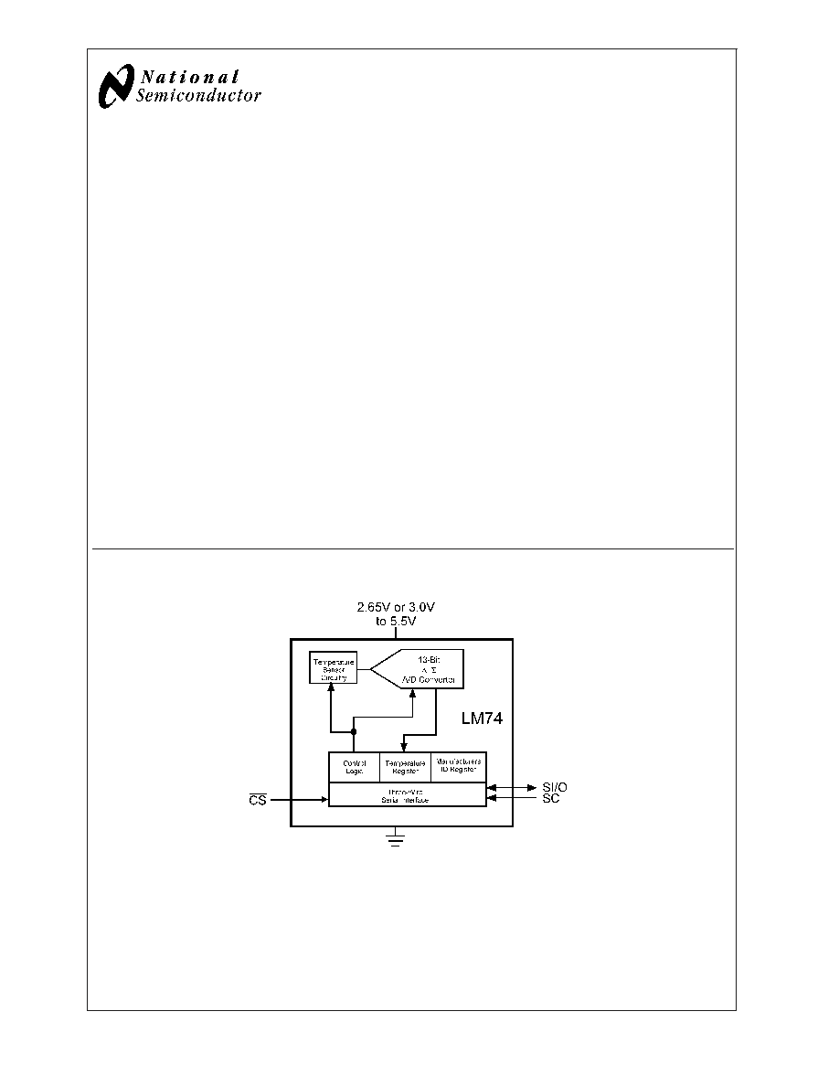
The LM74 is a temperature sensor, Delta-Sigma analog-to-
digital converter with an SPI and MICROWIRE compatible
interface. The host can query the LM74 at any time to read
temperature. A shutdown mode decreases power consump-
tion to less than 10 µA. This mode is useful in systems where
low average power consumption is critical.
The LM74 has 12-bit plus sign temperature resolution
(0.0625∞C per LSB) while operating over a temperature
range of -55∞C to +150∞C.
The LM74's 3.0V to 5.5V supply voltage range, low supply
current and simple SPI interface make it ideal for a wide
range of applications. These include thermal management
and protection applications in hard disk drives, printers, elec-
tronic test equipment, and office electronics. The LM74 is
available in the SO-8 package as well as an 5-Bump micro
SMD package.
Applications
n
System Thermal Management
n
Personal Computers
n
Disk Drives
n
Office Electronics
n
Electronic Test Equipment
Features
n
0.0625∞C temperature resolution.
n
Shutdown mode conserves power between temperature
reading
n
SPI and MICROWIRE Bus interface
n
5-Bump micro SMD package saves space
Key Specifications
j
Supply Voltage
3.0V or 2.65V to
5.5V
j
Supply Current
operating
265µA (typ)
520µA (max)
shutdown
3µA (typ)
j
Temperature
Accuracy
-10∞C to 65∞C
±
1.25∞C(max)
-25∞C to 110∞C
±
2.1∞C(max)
-55∞C to 125∞C
±
3∞C(max)
Simplified Block Diagram
10090901
MICROWIRE
Æ
is a registered trademark of National Semiconductor Corporation.
TRI-STATE
Æ
is a registered trademark of National Semiconductor Corporation.
April 2003
LM74
SPI/MICROWIRE
12-Bit
Plus
Sign
T
emperature
Sensor
© 2003 National Semiconductor Corporation
DS100909
www.national.com
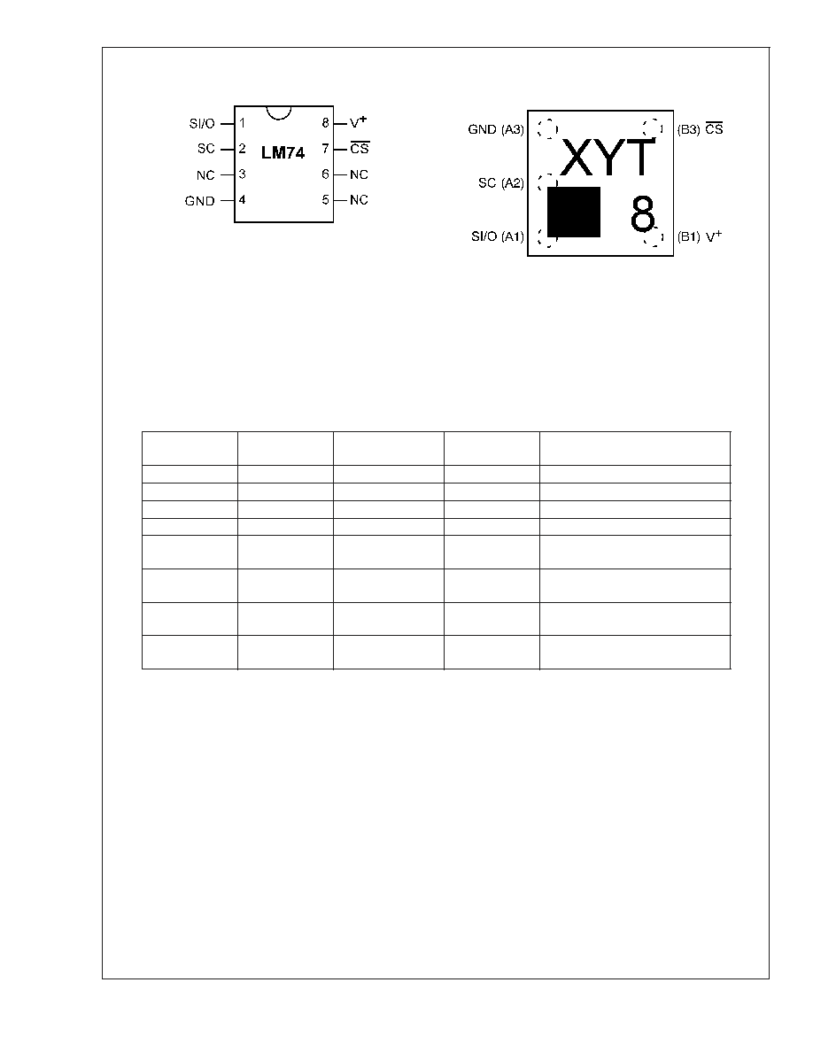
Connection Diagrams
SO-8
5-Bump micro SMD
10090902
TOP VIEW
NS Package Number M08A
10090924
Note:
-
Pin numbers are referenced to the package marking text orientation. Pin
1 is designated by the square.
-
Reference JEDEC Registration MO-211, variation BC
- The top 4 characters designate the date code. The bottom 3 characters
designate the device type (see ordering information).
TOP VIEW
NS Package Number BPD05MPB
Ordering Information
Order Number
Package
Marking
NS Package
Number
Supply Voltage
Transport Media
LM74CIM-3
LM74CIM-3
SO-8, M08A
3.0V to 3.6V
95 Units in Rail
LM74CIMX-3
LM74CIM-3
SO-8, M08A
3.0V to 3.6V
2500 Units in Tape and Reel
LM74CIM-5
LM74CIM-5
SO-8, M08A
4.5V to 5.5V
95 Units in Rail
LM74CIMX-5
LM74CIM-5
SO-8, M08A
4.5V to 5.5V
2500 Units in Tape and Reel
LM74CIBP-3
T8
micro SMD,
BPD05MPB
2.65V to 3.6V
250 Units in Tape and Reel
LM74CIBPX-3
T8
micro SMD,
BPD05MPB
2.65V to 3.6V
3000 Units in Tape and Reel
LM74CIBP-5
T9
micro SMD,
BPD05MPB
4.5V to 5.5V
250 Units in Tape and Reel
LM74CIBPX-5
T9
micro SMD,
BPD05MPB
4.5V to 5.5V
3000 Units in Tape and Reel
LM74
www.national.com
2
Pin Descriptions
Label
SO-8
Pin #
micro
SMD
Pin #
Function
Typical Connection
SI/O
1
1
Slave Input/Output - Serial bus bi-directional data
line. Schmitt trigger input.
From and to Controller
SC
2
5
Slave Clock - Serial bus clock Schmitt trigger input
line.
From Controller
NC
3
No Connection
No Connection
GND
4
4
Power Supply Ground
Ground
NC
5
No Connection
No Connection
NC
6
No Connection
No Connection
CS
7
3
Chip Select input.
From Controller
V
+
8
2
Positive Supply Voltage Input
DC Voltage from 3.0V to 5.5V for the
LM74CIM and 2.65V to 5.5V for the
LM74CIBP. Bypass with a 0.1 µF ceramic
capacitor.
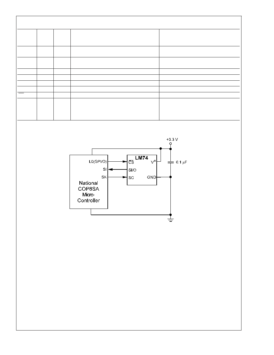
Typical Application
10090903
FIGURE 1. COP Microcontroller Interface
LM74
www.national.com
3
Absolute Maximum Ratings
(Note 1)
Supply Voltage
-0.3V to 6.0V
Voltage at any Pin
-0.3V to V
+
+ 0.3V
Input Current at any Pin (Note 2)
5 mA
Package Input Current (Note 2)
20 mA
Storage Temperature
-65∞C to +150∞C
Soldering Information, Lead Temperature
SO-8 Package (Note 3)
Vapor Phase (60 seconds)
Infrared (15 seconds)
215∞C
220∞C
ESD Susceptibility (Note 4)
Human Body Mode
LM74CIBP SC, pin 5
1900V
LM74CIM and LM74CIBP all
other pins
2000V
Machine Model
200V
Operating Ratings
Specified Temperature Range
T
MIN
to T
MAX
(Note 5)
LM74CIBP
LM74CIM
-40∞C to +125∞C
-55∞C to +150∞C
Supply Voltage Range (+V
S
)
LM74CIBP
+2.65V to +5.5V
LM74CIM
+3.0V to +5.5V
Temperature-to-Digital Converter Characteristics
Unless otherwise noted, these specifications apply for V
+
= 2.65V to 3.6V for the LM74CIBP -3, V
+
= 3.0V to 3.6V for the
LM74CIM -3 and V
+
= 4.5V to 5.5V for the LM74 -5 (Note 6). Boldface limits apply for T
A
= T
J
= T
MIN
to T
MAX
; all other lim-
its T
A
= T
J
=+25∞C, unless otherwise noted.
Parameter
Conditions
Typical
(Note 7)
LM74-5
Limits
(Note 8)
LM74-3
Limits
(Note 8)
Units
(Limit)
Temperature Error (Note 6)
T
A
= -10∞C to +65∞C
±
1.25
±
1.25
∞C (max)
T
A
= -25∞C to +110∞C
±
2.1
+2.65/-2.15
∞C (max)
T
A
= -40∞C to +85∞C
+2.65/-1.65
±
2.15
∞C (max)
T
A
= -40∞C to +110∞C
+2.65/
-2.0
+2.65/-2.15
∞C (max)
T
A
= -55∞C to +125∞C
±
3.0
±
3.5
∞C (max)
T
A
= -55∞C to +150∞C
±
5.0
±
5.0
∞C (max)
Resolution
13
Bits
Temperature
Conversion Time
SO-8
(Note 9)
280
425
425
ms (max)
micro SMD
(Note 9)
611
925
925
ms (max)
Quiescent Current
SO-8
Serial Bus Inactive
310
520
520
µA (max)
micro SMD
265
470
470
µA (max)
SO-8
Serial Bus Active
310
µA
micro SMD
310
µA
SO-8
Shutdown Mode,
V
+
= 3.3V
7
µA
micro SMD
3
µA
SO-8
Shutdown Mode,
V
+
= 5V
8
µA
micro SMD
4
µA
Logic Electrical Characteristics
DIGITAL DC CHARACTERISTICS Unless otherwise noted, these specifications apply for V
+
= 2.65V to 3.6V for the
LM74CIBP -3, V
+
= 3.0V to 3.6V for the LM74CIM -3 and V
+
= 4.5V to 5.5V for the LM74 -5 (Note 6). Boldface limits apply
for T
A
= T
J
= T
MIN
to T
MAX
; all other limits T
A
= T
J
=+25∞C, unless otherwise noted.
Symbol
Parameter
Conditions
Typical
(Note 7)
Limits
(Note 8)
Units
(Limit)
V
IN(1)
Logical "1" Input Voltage
V
+
x 0.7
V (min)
V
+
+ 0.3
V (max)
V
IN(0)
Logical "0" Input Voltage
-0.3
V (min)
V
+
x 0.3
V (max)
Input Hysteresis Voltage
V
+
= 3.0V to 3.6V
0.8
0.35
V (min)
V
+
= 4.5V to 5.5V
0.8
0.33
V (min)
I
IN(1)
Logical "1" Input Current
V
IN
= V
+
0.005
3.0
µA (max)
LM74
www.national.com
4
Logic Electrical Characteristics
(Continued)
DIGITAL DC CHARACTERISTICS Unless otherwise noted, these specifications apply for V
+
= 2.65V to 3.6V for the
LM74CIBP -3, V
+
= 3.0V to 3.6V for the LM74CIM -3 and V
+
= 4.5V to 5.5V for the LM74 -5 (Note 6). Boldface limits apply
for T
A
= T
J
= T
MIN
to T
MAX
; all other limits T
A
= T
J
=+25∞C, unless otherwise noted.
Symbol
Parameter
Conditions
Typical
(Note 7)
Limits
(Note 8)
Units
(Limit)
I
IN(0)
Logical "0" Input Current
V
IN
= 0V
-0.005
-3.0
µA (min)
C
IN
All Digital Inputs
20
pF
V
OH
High Level Output Voltage
I
OH
= -400 µA
2.4
V (min)
V
OL
Low Level Output Voltage
I
OL
= +2 mA
0.4
V (max)
I
O_TRI-STATE
TRI-STATE Output Leakage
Current
V
O
= GND
V
O
= V
+
-1
+1
µA (min)
µA
(max)
SERIAL BUS DIGITAL SWITCHING CHARACTERISTICS Unless otherwise noted, these specifications apply for V
+
= 2.65V
to 3.6V for the LM74CIBP -3, V
+
= 3.0V to 3.6V for the LM74CIM -3 and V
+
= 4.5V to 5.5V for the LM74 -5 (Note 6); C
L
(load
capacitance) on output lines = 100 pF unless otherwise specified. Boldface limits apply for T
A
= T
J
= T
MIN
to T
MAX
; all other
limits T
A
= T
J
= +25∞C, unless otherwise noted.
Symbol
Parameter
Conditions
Typical
(Note 7)
Limits
(Note 8)
Units
(Limit)
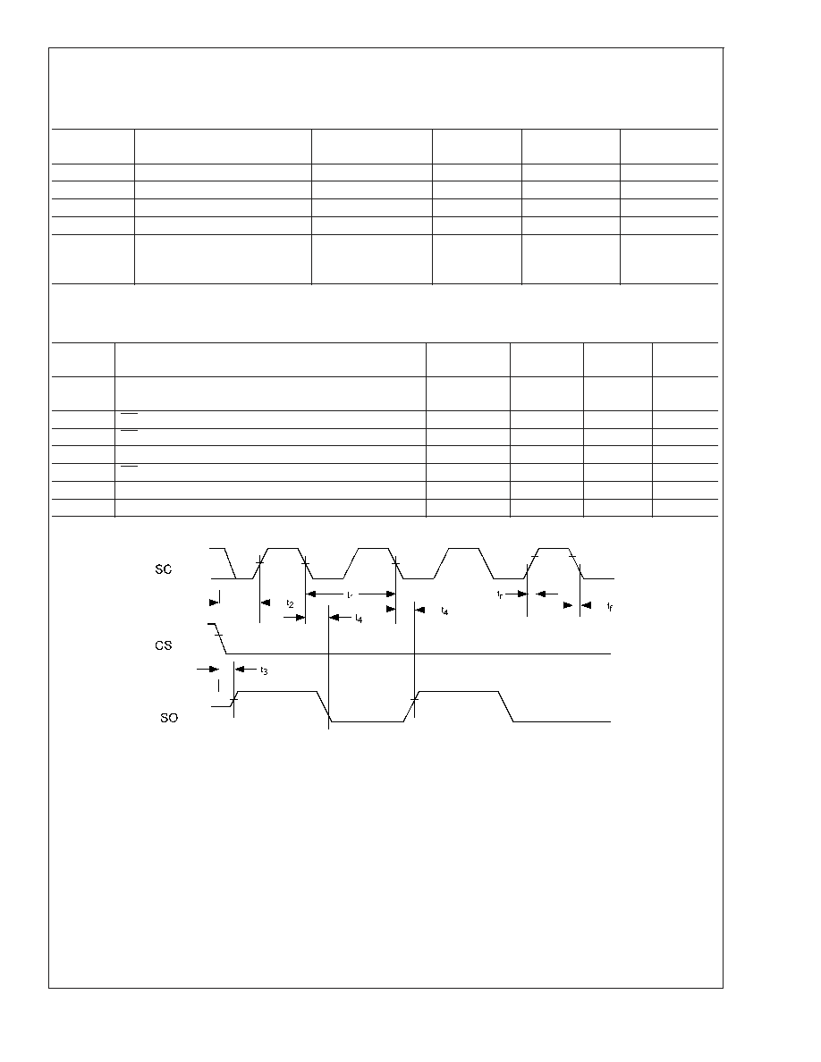
t
1
SC (Clock) Period
0.16
DC
µs (min)
(max)
t
2
CS Low to SC (Clock) High Set-Up Time
100
ns (min)
t
3
CS Low to Data Out (SO) Delay
70
ns (max)
t
4
SC (Clock) Low to Data Out (SO) Delay
100
ns (max)
t
5
CS High to Data Out (SO) TRI-STATE
200
ns (max)
t
6
SC (Clock) High to Data In (SI) Hold Time
50
ns (min)
t
7
Data In (SI) Set-Up Time to SC (Clock) High
30
ns (min)
10090904
FIGURE 2. Data Output Timing Diagram
LM74
www.national.com
5