LM74A
SPI/MICROWIRE
TM
12-Bit Plus Sign Temperature Sensor
(LM74 in Die Form)
General Description
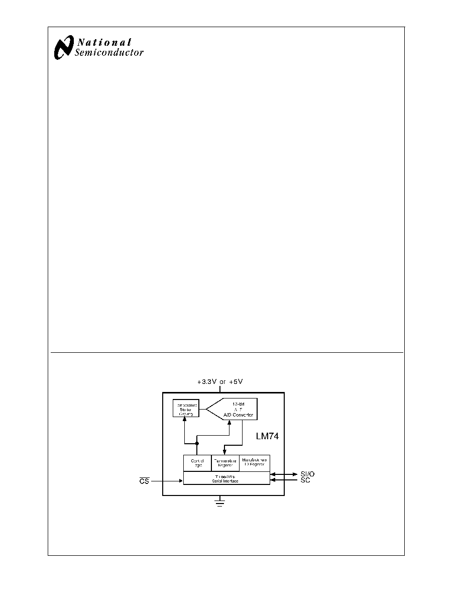
The LM74A is a temperature sensor, Delta-Sigma analog-to-
digital converter with an SPI and MICROWIRE compatible
interface in die form. The host can query the LM74A at any
time to read temperature. A shutdown mode decreases
power consumption to less than 10 µA. This mode is useful
in systems where low average power consumption is critical.
This particular data sheet applies to the LM74 in die form.
The LM74 is available in the SO-8 package as well as an
5-Bump micro SMD package please refer to LM74 data
sheet for detailed specifictions pertaining to the packaged
parts.
The LM74A has 12-bit plus sign temperature resolution
(0.0625∞C per LSB) while operating over a temperature
range of -40∞C to +150∞C. The LM74A-5 MDA accuracy of
±
3.5∞C is specified over a temperature range of 0∞C to
+150∞C.
The LM74A's 4.5V to 5.5V or 3.0V to 3.6V supply voltage
range, low supply current and simple SPI interface make it
ideal for a wide range of applications. These include thermal
management and protection applications in hard disk drives,
printers, electronic test equipment, and office electronics.
Applications
n
System Thermal Management
n
Personal Computers
n
Disk Drives
n
Office Electronics
n
Electronic Test Equipment
Features
n
0.0625∞C temperature resolution.
n
Shutdown mode conserves power between temperature
reading
n
SPI and MICROWIRE Bus interface
n
LM74 is also available in a 5-Bump micro SMD and
8-pin MSOP
Key Specifications
j
Supply Voltage
LM74A-5
4.5V to 5.5V
LM74A-3
3.0V to 3.6V
j
Supply Current
operating
310µA (typ)
520µA (max)
shutdown
8µA (typ)
j
LM74A-5 MDA
Temperature
Accuracy
0∞C to 140∞C
±
3.0∞C(max)
140∞C to 150∞C
±
3.5∞C(max)
Simplified Block Diagram
20017701
MICROWIRE
TM
is a trademark of National Semiconductor Corporation.
TRI-STATE
Æ
is a registered trademark of National Semiconductor Corporation.
November 2004
LM74A
SPI/MICROWIRE
12-Bit
Plus
Sign
T
emperature
Sensor
(LM74
in
Die
Form)
© 2004 National Semiconductor Corporation
DS200177
www.national.com
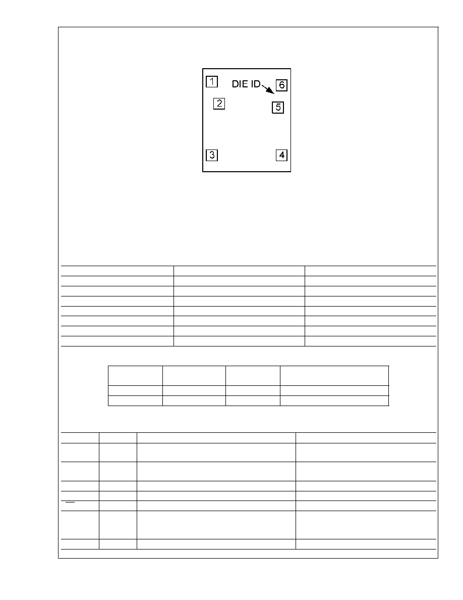
Connection Diagram
LM74A
Bond Pad Layout
20017727
TOP VIEW
1.40mm x 1.57 mm (55 x 62 mils)
Bond Pad Mechanical Dimensions
Dimensions of bond pad coordinates are in millimeters.
Origin of coordinates: center of die.
X-Direction is in the longitudinal axis of the die.
Coordinates refer to center of Bond Pad.
Pin#
X
Y
1
-0.569 mm
+0.585 mm
2
-0.537 mm
+0.314 mm
3
-0.569 mm
-0.554 mm
4
n/a
n/a
5
+0.537 mm
+0.277 mm
6
+0.569 mm
+0.569 mm
Back
Ordering Information
Order Number
NS Package
Number
Supply Voltage
Transport Media
LM74A-5 MDA
No Package, Die
4.5V to 5.5V
7k unit surftape tape-and-reel
LM74A-3 MDA
No Package, Die
3.0V to 3.6V
7k unit surftape tape-and-reel
Pin Descriptions
Label
Pin #
Function
Typical Connection
SI/O
1
Slave Input/Output - Serial bus bi-directional data
line. Shmitt trigger input.
From and to Controller
SC
2
Slave Clock - Serial bus clock Shmitt trigger input
line.
From Controller
GND
3
Power Supply Ground
Ground
NC
4
No Connection
No Connection
CS
5
Chip Select input.
From Controller
V
+
6
Positive Supply Voltage Input
DC Voltage from 4.5V to 5.5V for the
LM74A-5 and 3.0V to 3.6V for the LM74A-3.
Bypass with a 0.1 µF ceramic capacitor.
Back
(Backside)
Can go to GND connection
LM74A
www.national.com
2
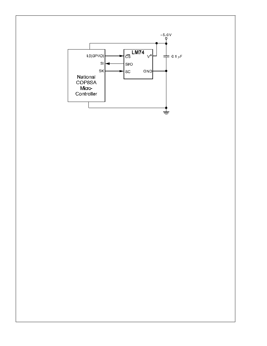
Typical Application
20017703
FIGURE 1. COP Microcontroller Interface
LM74A
www.national.com
3
Absolute Maximum Ratings
(Note 1)
Supply Voltage
-0.3V to 6.0V
Voltage at any Pin
-0.3V to V
+
+ 0.3V
Input Current at any Pin (Note 2)
5 mA
Package Input Current (Note 2)
20 mA
Storage Temperature
-65∞C to +150∞C
ESD Susceptibility (Note 3)
Human Body Mode
Machine Model
2000V
200V
Operating Ratings
Operating Temperature Range
-40∞C to +150∞C
Specified Temperature Range
T
MIN
to T
MAX
(Note 4)
LM74A
-40∞C to +150∞C
Supply Voltage Range (+V
S
)
LM74-5 MDA
+4.5V to +5.5V
LM74-3 MDA
+3.0V to +3.6V
Temperature-to-Digital Converter Characteristics
Unless otherwise noted, these specifications apply for V
+
= 4.5V to 5.5V for the LM74-5 MDA and V
+
= 3.0V to 3.6V for the
LM74-3 MDA.(Note 5). Boldface limits apply for T
A
= T
J
= T
MIN
to T
MAX
; all other limits T
A
= T
J
=+25∞C, unless otherwise
noted.
Parameter
Conditions
Typical
(Note 6)
LM74-5 MDA
Limits
(Note 7)
LM74-3 MDA
Limits
(Note 7)
Units
(Limit)
Temperature Error (Note 5)
T
A
= 0∞C to
+140∞C
±
3.0
∞C (max)
T
A
= +140∞C
to +150∞C
±
3.5
∞C (max)
T
A
= -40∞C to
+150∞C
±
5
∞C (max)
Resolution
13
Bits
Temperature Conversion Time
(Note 8)
280
425
ms (max)
Quiescent Current
Serial Bus
Inactive
310
520
µA (max)
Serial Bus
Active
310
µA
Shutdown
Mode, V
+
=
5V
8
µA
Logic Electrical Characteristics
DIGITAL DC CHARACTERISTICS Unless otherwise noted, these specifications apply for V
+
= 4.5V to 5.5V for the LM74-5
MDA and V
+
= 3.0V to 3.6V for the LM74-3 MDA.(Note 5). Boldface limits apply for T
A
= T
J
= T
MIN
to T
MAX
; all other limits
T
A
= T
J
=+25∞C, unless otherwise noted.
Symbol
Parameter
Conditions
Typical
(Note 6)
Limits
(Note 7)
Units
(Limit)
V
IN(1)
Logical "1" Input Voltage
V
+
x 0.7
V (min)
V
+
+ 0.3
V (max)
V
IN(0)
Logical "0" Input Voltage
-0.3
V (min)
V
+
x 0.3
V (max)
Input Hysteresis Voltage
V
+
= 4.5V to 5.5V
0.8
0.33
V (min)
I
IN(1)
Logical "1" Input Current
V
IN
= V
+
0.005
3.0
µA (max)
I
IN(0)
Logical "0" Input Current
V
IN
= 0V
-0.005
-3.0
µA (min)
C
IN
All Digital Inputs
20
pF
V
OH
High Level Output Voltage
I
OH
= -400 µA
V
+
x 0.7
V (min)
V
OL
Low Level Output Voltage
I
OL
= +2 mA
0.4
V (max)
I
O_TRI-STATE
TRI-STATE Output Leakage
Current
V
O
= GND
V
O
= V
+
-1
+1
µA (min)
µA
(max)
LM74A
www.national.com
4
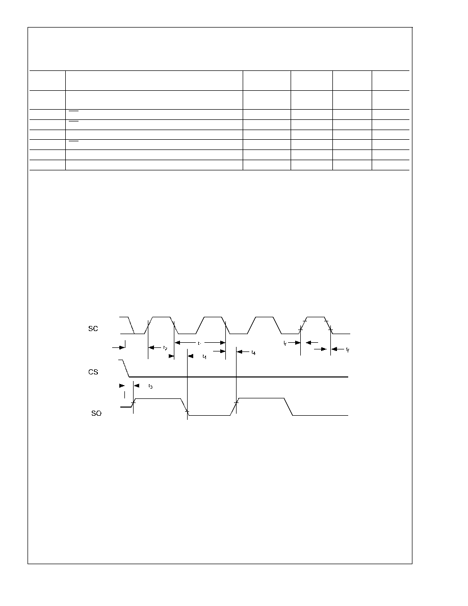
Serial Bus Digital Switching Characteristics
Unless otherwise noted, these specifications apply for V
+
= 4.5V to 5.5V for the LM74-5 MDA and V
+
= 3.0V to 3.6V for the
LM74-3 MDA.(Note 5). Boldface limits apply for T
A
= T
J
= T
MIN
to T
MAX
; all other limits T
A
= T
J
=+25∞C, unless otherwise
noted.
Symbol
Parameter
Conditions
Typical
(Note 6)
Limits
(Note 7)
Units
(Limit)
t
1
SC (Clock) Period
0.16
DC
µs (min)
(max)
t
2
CS Low to SC (Clock) High Set-Up Time
100
ns (min)
t
3
CS Low to Data Out (SO) Delay
70
ns (max)
t
4
SC (Clock) Low to Data Out (SO) Delay
100
ns (max)
t
5
CS High to Data Out (SO) TRI-STATE
200
ns (max)
t
6
SC (Clock) High to Data In (SI) Hold Time
50
ns (min)
t
7
Data In (SI) Set-Up Time to SC (Clock) High
30
ns (min)
Note 1: Absolute Maximum Ratings indicate limits beyond which damage to the device may occur. DC and AC electrical specifications do not apply when operating
the device beyond its rated operating conditions.
Note 2: When the input voltage (V
I
) at any pin exceeds the power supplies (V
I
<
GND or V
I
>
+V
S
) the current at that pin should be limited to 5 mA. The 20 mA
maximum package input current rating limits the number of pins that can safely exceed the power supplies with an input current of 5 mA to four.
Note 3: Human body model, 100 pF discharged through a 1.5 k
resistor. Machine model, 200 pF discharged directly into each pin.
Note 4: The life expectancy of the LM74A will be reduced when operating at elevated temperatures.
Note 5: All LM74A parts will function over the V
+
supply voltage range of 3V to 5.5V. The LM74A temperature error specifications for temperature ranges of 0∞C to
+140∞C, 0∞C to +150∞C and -40∞C to +150∞C include error induced by power supply variation of
±
10% from the nominal value of 5V or 3.3V.
Note 6: Typicals are at T
A
= 25∞C and represent most likely parametric norm.
Note 7: Limits are guaranteed to National's AOQL (Average Outgoing Quality Level).
Note 8: This specification is provided only to indicate how often temperature data is updated. The LM74A can be read at any time without regard to conversion state
(and will yield last conversion result). A conversion in progress will not be interrupted. The output shift register will be updated at the completion of the read and a
new conversion restarted.
Note 9: For best accuracy, minimize output loading. Higher sink currents can affect sensor accuracy with internal heating. This can cause an error of 0.64∞C at full
rated sink current and saturation voltage based on junction-to-ambient thermal resistance.
Timing Diagrams
20017704
FIGURE 2. Data Output Timing Diagram
LM74A
www.national.com
5