LM80
Serial Interface ACPI-Compatible Microprocessor System
Hardware Monitor
General Description
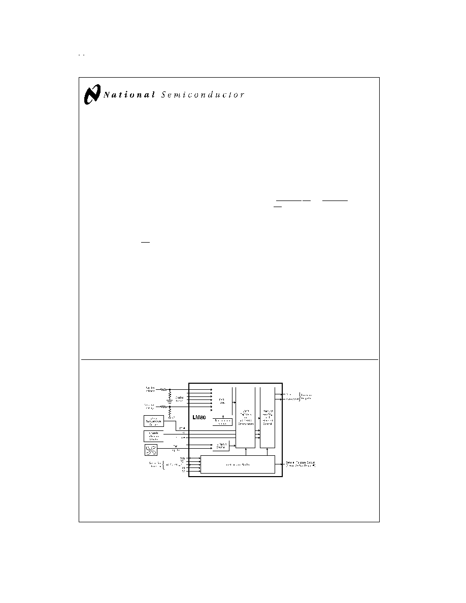
The LM80 provides 7 positive voltage inputs, temperature
measurement, fan speed measurement, and hardware
monitoring on an I
2
C
TM
interface. The LM80 performs
WATCHDOG
TM
comparisons of all measured values and an
open-drain interrupt output becomes active when any values
exceed programmed limits. A Chassis Intrusion input is pro-
vided to monitor and reset an external circuit designed to
latch a chassis intrusion event.
The LM80 is especially suited to interface to both linear and
digital temperature sensors. The 10 mV LSB and 2.56 volt
input range is ideal for accepting inputs from a linear sensor
such as the LM50. The BTI is used as an input from either
digital or thermostat sensors such as LM75 and LM56.
The LM80's 2.8V to 5.75V supply voltage range, low supply
current, and I
2
C interface make it ideal for a wide range of
applications. These include hardware monitoring and protec-
tion applications in personal computers, electronic test
equipment, and office electronics.
Features
n
Temperature sensing
n
7 positive voltage inputs
n
2 programmable fan speed monitoring inputs
n
10 mV LSB and 2.56V input range accepts outputs from
linear temperature sensors such as the LM50
n
Chassis Intrusion Detector input
n
WATCHDOG comparison of all monitored values
n
Separate input to show status in Interrupt Status
Register of additional external temperature sensors such
as the LM56 or LM75
n
I
2
C Serial Bus interface compatibility
n
Shutdown mode to minimize power consumption
n
Programmable RST_OUT/OS pin: RST_OUT provides a
Reset output; OS provides an Interrupt Output activated
by an Overtemperature Shutdown event
Key Specifications
n
Voltage monitoring Error
±
1% (max)
n
Temperature Error
-25∞C to +125∞C
±
3∞C (max)
n
Supply Voltage Range
2.8V to
5.75V
n
Supply Current
Operating:
0.2 mA typ
Shutdown:
15 µA typ
n
ADC Resolution
8 Bits
n
Temperature Resolution
0.5∞C
Applications
n
System Thermal and Hardware Monitoring for Servers
and PCs
n
Office Electronics
n
Electronic Test Equipment and Instrumentation
Typical Application
TRI-STATE
Æ
is a registered trademark of National Semiconductor Corporation.
WATCHDOG
TM
is a trademark of National Semiconductor Corporation.
I2C
Æ
is a registered trademark of the Philips Corporation.
DS100040-1
# Indicates Active Low ("Not")
June 1999
LM80
Serial
Interface
ACPI-Compatible
Microprocessor
System
Hardware
Monitor
© 1999 National Semiconductor Corporation
DS100040
www.national.com
Ordering Information
Temperature Range
NS
Package
Number
-25∞C
T
A
+125∞C
Specified
Power
Supply
Voltage
Order Number
Device
Marking
LM80CIMT-3
1
LM80CIMTX-3
2
LM80CIMT-3
MTC24B
3.3V
LM80CIMT-5
1
LM80CIMTX-5
2
LM80CIMT-5
MTC24B
5.0V
Note:
1
-Rail transport media, 62 parts per rail
2
-Tape and reel transport media, 3400 parts per reel
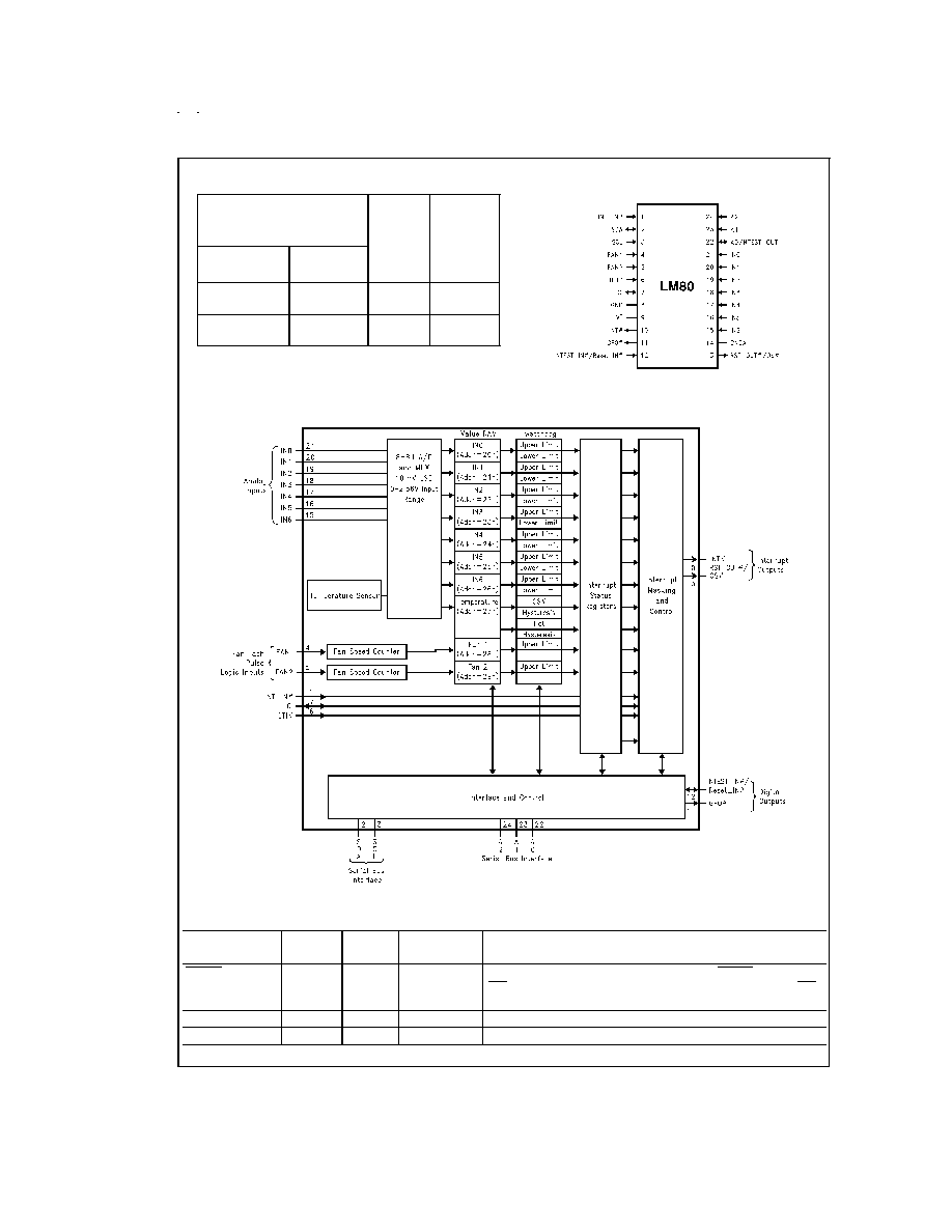
Connection Diagram
Block Diagram
Pin Descriptions
Pin
Name(s)
Pin
Number
Number
of Pins
Type
Description
INT_IN
1
1
Digital Input
This is an active low input that propagates the INT_IN signal to the
INT output of the LM80 via Interrupt Mask Register 1 Bit 7 and INT
enable Bit 1 of the Configuration Register.
SDA
2
1
Digital I/O
Serial Bus bidirectional Data. Open-drain output.
SCL
3
1
Digital Input
Serial Bus Clock.
DS100040-2
DS100040-3
www.national.com
2

Pin Descriptions
(Continued)
Pin
Name(s)
Pin
Number
Number
of Pins
Type
Description
FAN1-FAN2
4-5
2
Digital Inputs
0 to V
+
fan tachometer inputs.
BTI
6
1
Digital Input
Board Temperature Interrupt driven by O.S. outputs of additional
temperature sensors such as LM75. Provides internal pull-up of
10 k
.
CI (Chassis
Intrusion)
7
1
Digital I/O
An active high input from an external circuit which latches a Chassis
Intrusion event. This line can go high without any clamping action
regardless of the powered state of the LM80. The LM80 provides an
internal open drain on this line, controlled by Bit 5 of the
Configuration Register, to provide a minimum 10 ms reset of this
line.
GND
8
1
GROUND
Internally connected to all of the digital circuitry.
V
+
(+2.8V to
+5.75V)
9
1
POWER
+3.3V or +5V V
+
power. Bypass with the parallel combination of
10 µF (electrolytic or tantalum) and 0.1 µF (ceramic) bypass
capacitors.
INT
10
1
Digital Output
Non-Maskable Interrupt (open source)/Interrupt Request (open
drain). The mode is selected with Bit 5 of the Configuration Register
and the output is enabled when Bit 1 of the Configuration Register
is set to 1. The default state is disabled.
GPO (Power
Switch Bypass)
11
1
Digital Output
An active low open drain output intended to drive an external
P-channel power MOSFET for software power control.
NTEST_IN/
RESET_IN
12
1
Digital Input
An active-low input that enables NAND Tree board-level connectivity
testing. Refer to Section 10.0 on NAND Tree testing. Whenever
NAND Tree connectivity is enabled the LM80 is also reset to its
power on state.
RST_OUT/OS
13
1
Digital Output
Master Reset, 5 mA driver (open drain), active low output with a
10 ms minimum pulse width. Available when enabled via Bit 4 in
Configuration Register and Bit 7 of the Fan Divisor/RST_OUT/OS
Register. Bit 6 of the Fan Divisor/RST_OUT/OS Register enables
this output as an active low Overtemperature Shutdown (OS).
GNDA
14
1
GROUND
Internally connected to all analog circuitry. The ground reference for
all analog inputs. This pin needs to be taken to a low noise analog
ground plane for optimum performance.
IN6-IN0
15-21
7
Analog Inputs
0V to 2.56V full scale range Analog Inputs.
A0/NTEST_OUT
22
1
Digital I/O
The lowest order bit of the Serial Bus Address. This pin functions as
an output when doing a NAND Tree test.
A1-A2
23-24
2
Digital Inputs
The two highest order bits of the Serial Bus Address.
TOTAL PINS
24
www.national.com
3
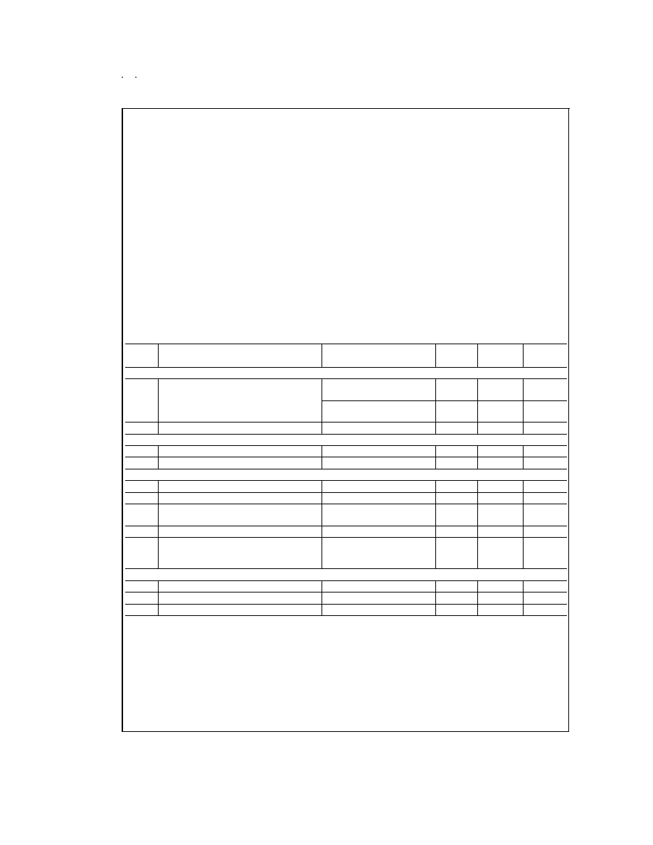
Absolute Maximum Ratings
(Notes 1, 2)
If Military/Aerospace specified devices are required,
please contact the National Semiconductor Sales Office/
Distributors for availability and specifications.
Positive Supply Voltage (V
+
)
6.5V
Voltage on Any Input or Output Pin
-0.3V to (V
+
+0.3V)
Ground Difference (GND - GNDA)
±
300 mV
Input Current at any Pin (Note 3)
±
5 mA
Package Input Current (Note 3)
±
20 mA
Maximum Junction Temperature
(T
J
max)
150∞C
ESD Susceptibility(Note 5)
Human Body Model
2000V
Machine Model
125V
Soldering Information
MTC24B Package (Note 6) :
Vapor Phase (60 seconds)
215∞C
Infrared (15 seconds)
235∞C
Storage Temperature
-65∞C to +150∞C
Operating Ratings
(Notes 1, 2)
Operating Temperature Range
T
MIN
T
A
T
MAX
LM80CIMT-3, LM80CIMT-5
-25∞C
T
A
+125∞C
Specified Temperature Range
T
MIN
T
A
T
MAX
LM80CIMT-3, LM80CIMT-5
-25∞C
T
A
+125∞C
Junction to Ambient Thermal Resistance (
JA
(Note 4) )
NS Package Number: MTC24B
95∞C/W
Supply Voltage (V
+
)
+2.8V to +5.75V
Ground Difference
(|GND - GNDA|)
100 mV
V
IN
Voltage Range:
-0.05V to V
+
+ 0.05V
DC Electrical Characteristics
The following specifications apply for +2.8 V
DC
V
+
+3.8 V
DC
for LM80CIMT-3, +4.25 V
DC
V
+
+5.75 V
DC
for LM80CIMT-5,
IN0-IN6 R
S
= 25
, unless otherwise specified. Boldface limits apply for T
A
= T
J
= T
MIN
to T
MAX
; all other limits T
A
= T
J
=
25∞C.(Note 7)
Symbol
Parameter
Conditions
Typical
Limits
Units
(Note 8)
(Note 9)
(Limits)
POWER SUPPLY CHARACTERISTICS
I
+
Supply Current
Interface Inactive and
V
+
= 5.75V
0.2
2.0
mA (max)
Interface Inactive and
V
+
= 3.8V
0.18
1.5
mA (max)
Shutdown Mode
15
µA
TEMPERATURE-to-DIGITAL CONVERTER CHARACTERISTICS
Temperature Error
-25∞C
T
A
+125∞C
±
3
∞C (max)
Resolution
0.5
∞C (min)
ANALOG-to-DIGITAL CONVERTER CHARACTERISTICS
Resolution (8 bits with full-scale at 2.56V)
10
mV
TUE
Total Unadjusted Error
(Note 10)
±
1
% (max)
DNL
Differential Non-Linearity
±
1
LSB
(max)
PSS
Power Supply Sensitivity
±
1
%/V
t
C
Total Monitoring Cycle Time
(Note 11)
9-bit Temp resolution
12-bit Temp resolution
1.0
1.5
2
sec (max)
sec (max)
MULTIPLEXER/ADC INPUT CHARACTERISTICS
On Resistance
0.5
10
k
(max)
Input Current (On Channel Leakage Current)
±
1
µA
Off Channel Leakage Current
±
1
µA
www.national.com
4
DC Electrical Characteristics
(Continued)
The following specifications apply for +2.8 V
DC
V
+
+3.8 V
DC
for LM80CIMT-3, +4.25 V
DC
V
+
+5.75 V
DC
for LM80CIMT-5,
IN0-IN6 R
S
= 25
, unless otherwise specified. Boldface limits apply for T
A
= T
J
= T
MIN
to T
MAX
; all other limits T
A
= T
J
=
25∞C.(Note 7)
Symbol
Parameter
Conditions
Typical
Limits
Units
(Note 8)
(Note 9)
(Limits)
FAN RPM-to-DIGITAL CONVERTER
Fan RPM Error
+25∞C
T
A
+75∞C
±
10
% (max)
-10∞C
T
A
+100∞C
±
15
% (max)
-25∞C
T
A
+125∞C
±
20
% (max)
Full-scale Count
255
(max)
FAN1 and FAN2 Nominal Input
RPM (See
Section 6.0)
Divisor = 1, Fan Count = 153
(Note 12)
8800
RPM
Divisor = 2, Fan Count = 153
(Note 12)
4400
RPM
Divisor = 3, Fan Count = 153
(Note 12)
2200
RPM
Divisor = 4, Fan Count = 153
(Note 12)
1100
RPM
Internal Clock Frequency
+25∞C
T
A
+75∞C
22.5
20.2
kHz (min)
24.8
kHz (max)
-10∞C
T
A
+100∞C
22.5
19.1
kHz (min)
25.9
kHz (max)
-25∞C
T
A
+125∞C
22.5
18
kHz (min)
27
kHz (max)
DIGITAL OUTPUTS: A0/NTEST_OUT, INT
V
OUT(1)
Logical "1" Output Voltage
I
OUT
= +5.0 mA at
V
+
= +4.25V, I
OUT
= +3.0 mA
at V
+
= +2.8V
2.4
V (min)
V
OUT(0)
Logical "0" Output Voltage
I
OUT
= -5.0 mA at
V
+
= +5.75V, I
OUT
= -3.0 mA
at V
+
= +3.8V
0.4
V (max)
OPEN DRAIN OUTPUTS: GPO, RST_OUT/OS, CI
V
OUT(0)
Logical "0" Output Voltage
I
OUT
=- 5.0 mA
at V
+
= +5.75V,
I
OUT
= -3.0 mA at V
+
= +3.8V
0.4
V (min)
I
OH
High Level Output Current
V
OUT
= V
+
0.1
100
µA (max)
RST_OUT/OS, CI
30
10
ms (min)
Pulse Width
OPEN DRAIN SERIAL BUS OUTPUT: SDA
V
OUT(0)
Logical "0" Output Voltage
I
OUT
= -3.0 mA at
V
+
= +5.75V, I
OUT
= -3.0 mA
at V
+
= +3.8V
0.4
V (min)
I
OH
High Level Output Current
V
OUT
= V
+
0.1
100
µA (max)
DIGITAL INPUTS: A0/NTEST_Out, A1-A2, BTI, CI (Chassis Intrusion), INT_IN, and NTEST_IN/Reset_IN
V
IN(1)
Logical "1" Input Voltage
2.0
V (min)
V
IN(0)
Logical "0" Input Voltage
0.8
V (max)
SERIAL BUS INPUTS (SCL, SDA) and FAN TACH PULSE INPUTS (FAN1, FAN2)
V
IN(1)
Logical "1" Input Voltage
0.7 x V
+
V (min)
V
IN(0)
Logical "0" Input Voltage
0.3 x V
+
V (max)
ALL DIGITAL INPUTS Except for BTI
I
IN(1)
Logical "1" Input Current
V
IN
= V
+
-0.005
-1
µA (min)
I
IN(0)
Logical "0" Input Current
V
IN
= 0 V
DC
0.005
1
µA (max)
C
IN
Digital Input Capacitance
20
pF
www.national.com
5