 | ÐлекÑÑоннÑй компоненÑ: LM8207 | СкаÑаÑÑ:  PDF PDF  ZIP ZIP |
Äîêóìåíòàöèÿ è îïèñàíèÿ www.docs.chipfind.ru
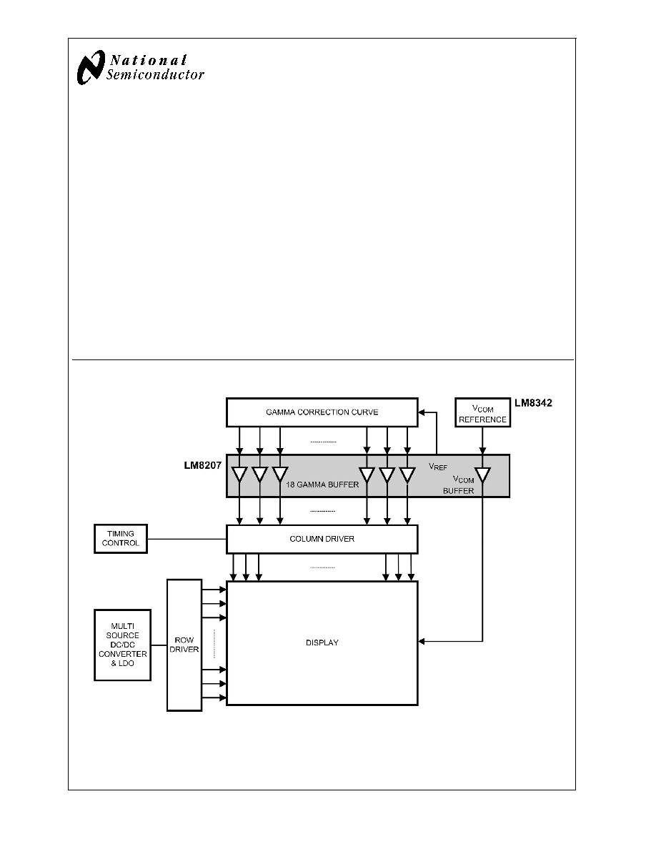
LM8207
TFT 18 Gamma Buffer + V
COM
Driver + Voltage Reference
General Description
The LM8207 is a combination of 18-channel gamma buffers,
a V
COM
driver and a temperature compensated internal volt-
age reference. It is designed for buffering voltage levels and
driving high capacitive loads in large TFT panels. The
gamma buffers are individually optimized to the input/output
requirements of their respective gamma position to cover the
whole voltage range from rail to rail. Any desired gamma
correction curve can be obtained by combining the gamma
buffers with external resistors. The V
COM
driver has a high
output current capability and is stable with large capacitive
loads, typical for large panel sizes. This will result in a fast
recovery time for large voltage variations at the output. The
internal band gap reference can be used to form a highly
stable voltage to generate the gamma correction voltages. In
combination with the internal amplifier, the reference voltage
can be programmed to voltages up to the positive rail. The
LM8207 is offered in a 48-pin TSSOP package.
Features
n
Gamma buffers 1-2 swing to V
DD
n
Gamma buffers 17-18 swing to V
SS
n
Large output current V
COM
driver (I
SC
= 300 mA)
n
Stable (1%) internal 1.295V reference, to improve
picture quality and reduce variations
n
48-pin TSSOP package
Applications
n
TFT gamma curve connection and V
COM
voltage
buffering
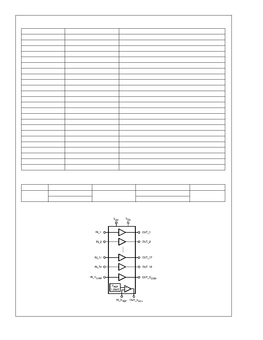
TFT Panel Block Diagram
20137926
September 2005
LM8207
TFT
18
Gamma
Buffer
+
V
COM
Driver
+
V
oltage
Reference
© 2005 National Semiconductor Corporation
DS201379
www.national.com
Absolute Maximum Ratings
(Notes 1, 2)
If Military/Aerospace specified devices are required,
please contact the National Semiconductor Sales Office/
Distributors for availability and specifications.
ESD Tolerance (Note 3)
Human Body
2.5 kV
Machine Model
250V
Supply Voltage (V
DD
- V
SS
)
18V
Storage Temperature Range
-65°C to +150°C
Junction Temperature (Note 4)
+150°C
Soldering Information
Infrared or Convection (20 sec.)
230°C
Wave Soldering (10 sec.)
260°C
Operating Ratings
(Note 1)
Operating Temperature Range
-40°C to +105°C
Operating Voltage Range
6V to 16V
Package Thermal Resistance,
JA
(Note 4)
48-Pin TSSOP
84°C/W
16V Electrical Characteristics
Unless otherwise specified, all limits guaranteed for T
J
= 25°C, V
DD
= 16V, V
SS
= 0V, & C
LOAD
= 100 pF (Gamma & V
COM
Buffers). Boldface limits apply at the temperature extremes. (Note 5)
Symbol
Parameter
Conditions
Min
(Note 6)
Typ
(Note 7)
Max
(Note 6)
Units
Gamma Buffers
BW_Gamma
-3 dB Bandwidth
2
MHz
SR_Gamma
Slew Rate (Note 8)
1
V/µs
T
REC
_Gamma
Output Recovery Time (Note 9)
400
ns
V
IN
_Gamma
Input Voltage Range
Buffer 1-2
Positive
V
DD
V
Negative
V
SS
+0.6
Buffer 3-8 & 11-16
Positive
V
DD
-0.6
Negative
V
SS
+0.6
Buffer 9
Positive
V
DD
-0.6
Negative
V
SS
Buffer 10
Positive
V
DD
-0.6
Negative
V
SS
+0.6
Buffer 17-18
Positive
V
DD
-0.6
Negative
V
SS
V
OUT
_Gamma
Output Voltage Range
Buffer 1-2,
No Load
Positive
V
DD
-0.25
V
DD
-0.1
V
Negative
V
SS
+1.5
V
SS
+1.6
Buffer 3-8 & 11-16
No Load
Positive
V
DD
-1.2
V
DD
-1.1
Negative
V
SS
+0.6
V
SS
+0.7
Buffer 9,
No Load
Positive
V
DD
-1.0
V
DD
-0.8
Negative
V
SS
+0.8
V
SS
+0.9
Buffer 10,
No Load
Positive
V
DD
1.2
V
DD
1.1
Negative
V
SS
+0.6
V
SS
+0.7
Buffer 17-18,
No Load
Positive
V
DD
1.6
V
DD
1.5
Negative
V
SS
+0.1
V
SS
+0.25
I
BIAS
_Gamma
Absolute, Input Bias Current
Within Gamma Buffer Output
Voltage Range
30
nA
V
OS
_Gamma
Input Offset Voltage
Buffer 1-2, V
IN
= 8V
5
10
mV
Buffer 3-8, 11-16, V
IN
= 8V
1
5
Buffer 9, V
IN
= 8V
1
5
Buffer 10, V
IN
= 8V
1
5
Buffer 17-18, V
IN
= 8V
5
10
LM8207
www.national.com
2
16V Electrical Characteristics
(Continued)
Unless otherwise specified, all limits guaranteed for T
J
= 25°C, V
DD
= 16V, V
SS
= 0V, & C
LOAD
= 100 pF (Gamma & V
COM
Buffers). Boldface limits apply at the temperature extremes. (Note 5)
Symbol
Parameter
Conditions
Min
(Note 6)
Typ
(Note 7)
Max
(Note 6)
Units
I
OUT
_Gamma
Linear Output Current
(Note 10)
Buffer 1-2
Sourcing
20
46
mA
Sinking
0.2
0.33
Buffer 3-8 & 11-16
Sourcing
10
24.5
Sinking
3.5
5.5
Buffer 9
Sourcing
4.5
9.4
Sinking
15
27
Buffer 10
Sourcing
23
34.8
Sinking
3.5
5.5
Buffer 17-18
Sourcing
0.2
0.33
Sinking
20
50
PSRR
Power Supply Rejection Ratio
V
DD
- V
SS
= 6V to 16V
75
88
dB
V
COM
Driver
BW_V
COM
Bandwidth
10
MHz
SR_ V
COM
Slew Rate (Note 8)
4.5
V/µs
T_
REC
_V
COM
Output Recovery Time (Note 9)
200
ns
V
IN
_V
COM
Input Voltage Range
Positive
V
DD
V
Negative
V
SS
+0.6
V
OUT
_V
COM
Output Voltage Range
No Load
Positive
V
DD
1.0
V
DD
0.7
V
Negative
V
SS
+0.9
V
SS
+1.2
I
BIAS
_V
COM
Input Bias Current
Within V
COM
Buffer Output
Voltage Range
50
nA
V
OS
_V
COM
Input Offset Voltage
V
IN
= 8 V
1
10
mV
I
OUT
_
LIN
_V
COM
Linear Output Current
(Notes 10, 11)
Sourcing
160
mA
Sinking
150
I
OUT
_SC_V
COM
Short Circuit Output Current
(Notes 11, 12)
Sourcing
220
300
mA
Sinking
220
300
PSRR
Power Supply Rejection Ratio
V
DD
- V
SS
= 6V to 16V
75
88
dB
Voltage Reference Section
V
REF
Voltage
No Load
1.28
1.295
1.31
V
Reg
LOAD
Load Regulation
I
OUT
= 0 to 10 mA
0.14
mV/mA
V
REF_ACC
Voltage Accuracy
No Load, V
REF
= 1.295V
1
%
V
REF_MAX
Max Programming Range
I
OUT
= 4 mA
V
DD
-0.3
V
I
IN
_V
REF
Input Bias Current
Within V
REF
Output Voltage
Range
10
50
nA
TC_V
REF
Temperature Stability
70
ppm/°C
I
OUT
_V
REF
Max Output Current
Sourcing, V
OUT
= 1.295 V
71
mA
PSRR
Power Supply Rejection Ratio
(Line Regulation)
70
80
dB
Miscellaneous
I
S
Supply Current
4.5
6.5
8.5
9.5
mA
Note 1: Absolute Maximum Ratings indicate limits beyond which damage to the device may occur. Operating Ratings indicate conditions for which the device is
intended to be functional, but specific performance is not guaranteed. For guaranteed specifications, see the Electrical Characteristics tables.
Note 2: When the output of the V
COM
buffer exceeds the supply rails, while sinking or sourcing 100 mA, the V
COM
output is susceptible to latch.
Note 3: Human body model, 1.5 k
in series with 100 pF. Machine model, 0 in series with 200 pF
Note 4: The maximum power dissipation is a function of T
J(MAX)
,
JA
and T
A
. The maximum allowable power dissipation at any ambient temperature
is P
D
= (T
J(MAX)
T
A
)/
JA
. All numbers apply for packages soldered directly onto a PC board.
Note 5: Electrical Table values apply only for factory testing conditions at the temperature indicated. Factory testing condition result in very limited self-heating of
the device such that T
J
= T
A
. No guarantee of parametric performance is indicated in the electrical table under conditions of internal self-heating where T
J
>
T
A
.
LM8207
www.national.com
3
16V Electrical Characteristics
(Continued)
Note 6: All limits are guaranteed by design or statistical analysis.
Note 7: Typical values represent the parametric norm at the time of characterization.
Note 8: Slew Rate is measured for V
IN
= 4 V
PP
. 10% -90% values are used. Slew rate is the average of the rising and falling slew rates
Note 9: 4 V
PP
pulse (50 ns rise time) applied to one side of 100 pF series output capacitance, other side connected to output of buffer. Output to within 0.1% of
input voltage.
Note 10: Linear output current measured at |V
OUT
- V
IN
| = 0.1V.
Note 11: This is a momentary test. Continuous large output currents may result in exceeding the maximum power dissipation and damage the device.
Note 12: Short circuit current measured at |V
OUT
- V
IN
| = 1V.
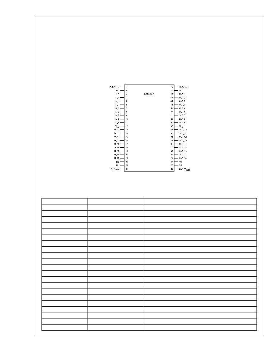
Connection Diagram
48-Pin TSSOP
20137902
Top View
Pin Descriptions
Pin #
Description
Remark
1
OUT_V
REF
Reference voltage amplifier output
2
NC
No connection
3
IN_1
Input gamma buffer 1
4
IN_2
Input gamma buffer 2
5
IN_3
Input gamma buffer 3
6
IN_4
Input gamma buffer 4
7
IN_5
Input gamma buffer 5
8
IN_6
Input gamma buffer 6
9
IN_7
Input gamma buffer 7
10
IN_8
Input gamma buffer 8
11
IN_9
Input gamma buffer 9
12
V
DD
Positive supply voltage (V
DD
)
13
IN_10
Input gamma buffer 10
14
IN_11
Input gamma buffer 11
15
IN_12
Input gamma buffer 12
16
IN_13
Input gamma buffer 13
17
IN_14
Input gamma buffer 14
18
IN_15
Input gamma buffer 15
19
IN_16
Input gamma buffer 16
20
IN_17
Input gamma buffer 17
21
IN_18
Input gamma buffer 18
LM8207
www.national.com
4
Pin Descriptions
(Continued)
22,23
NC
No connection
24
IN_V
COM
Input V
COM
25
OUT_V
COM
Output V
COM
26,27
NC
No connection
28
OUT_18
Output gamma buffer 18
29
OUT_17
Output gamma buffer 17
30
OUT_16
Output gamma buffer 16
31
OUT_15
Output gamma buffer 15
32
OUT_14
Output gamma buffer 14
33
OUT_13
Output gamma buffer 13
34
OUT_12
Output gamma buffer 12
35
OUT_11
Output gamma buffer 11
36
OUT_10
Output gamma buffer 10
37
V
SS
Negative supply voltage (V
SS
)
38
OUT_9
Output gamma buffer 9
39
OUT_8
Output gamma buffer 8
40
OUT_7
Output gamma buffer 7
41
OUT_6
Output gamma buffer 6
42
OUT_5
Output gamma buffer 5
43
OUT_4
Output gamma buffer 4
44
OUT_3
Output gamma buffer 3
45
OUT_2
Output gamma buffer 2
46
OUT_1
Output gamma buffer 1
47
NC
No connection
48
IN_V
REF
Reference voltage amplifier feedback input
Ordering Information
Package
Part Number
Package Marking
Transport Media
NSC Drawing
48-Pin TSSOP
LM8207MT
LM8207MT
38 Units/Rail
MTD48
LM8207MTX
1k Units Tape and Reel
Block Diagram
20137901
LM8207
www.national.com
5
Document Outline