LM87
Serial Interface System Hardware Monitor with Remote
Diode Temperature Sensing
General Description
The LM87 is a highly integrated data acquisition system for
hardware monitoring of servers, Personal Computers, or vir-
tually any microprocessor-based system. In a PC, the LM87
can be used to monitor power supply voltages, motherboard
and processor temperatures, and fan speeds. Actual values
for these inputs can be read at any time. Programmable
WATCHDOG
TM
limits in the LM87 activate a fully program-
mable and maskable interrupt system with two outputs (INT#
and THERM#).
The LM87 has an on-chip digital output temperature sensor
with 8-bit resolution as well as the capability of monitoring 2
external diode temperatures to 8-bit resolution, an 8 channel
analog input ADC with 8-bit resolution and an 8-bit DAC. A
channel on the ADC measures the supply voltage applied to
the LM87, nominally 3.3 V. Two of the ADC inputs can be re-
directed to a counter that can measure the speed of up to 2
fans. A slow speed
ADC architecture allows stable mea-
surement of signals in an extremely noisy environment. The
DAC, with a 0 to 2.5 V output voltage range, can be used for
fan speed control. Additional inputs are provided for Chassis
Intrusion detection circuits, and VID monitor inputs. The VID
monitor inputs can also be used as IRQ inputs if VID moni-
toring is not required. The LM87 has a Serial Bus interface
that is compatible with SMBus
TM
and I
2
C
TM
.
Features
n
Remote diode temperature sensing (2 channels)
n
8 positive voltage inputs with scaling resistors for
monitoring +5 V, +12 V, +3.3 V, +2.5 V, Vccp power
supplies directly
n
2 inputs selectable for fan speed or voltage monitoring
n
8-bit DAC output for controlling fan speed
n
Chassis Intrusion Detector input
n
WATCHDOG
TM
comparison of all monitored values
n
SMBus or I
2
C Serial Bus interface compatibility
n
VID0-VID4 or IRQ0-IRQ4 monitoring inputs
n
On chip temperature sensor
Key Specifications
n
Voltage Monitoring Error
±
2 % (max)
n
External Temperature Error
±
4 ∞C (max)
n
Internal Temperature Error
-40 ∞C to +125 ∞C
±
3 ∞C (typ)
n
Supply Voltage Range
2.8 to 3.8 V
n
Supply Current
0.7 mA (typ)
n
ADC and DAC Resolution
8 Bits
n
Temperature Resolution
1.0 ∞C
Applications
n
System Thermal and Hardware Monitoring for Servers,
Workstations and PCs
n
Networking and Telecom Equipment
n
Office Electronics
n
Electronic Test Equipment and Instrumentation
Ordering Information
Temperature Range
NS Package
Number
-40 ∞C
T
A
+125 ∞C
Order Number
Device Marking
LM87CIMT
1
LM87CIMT
MTC24B
LM87CIMTX
2
LM87CIMT
MTC24B
Note:
1
-Rail transport media, 61 parts per rail
2
-Tape and reel transport media, 2500 parts per reel
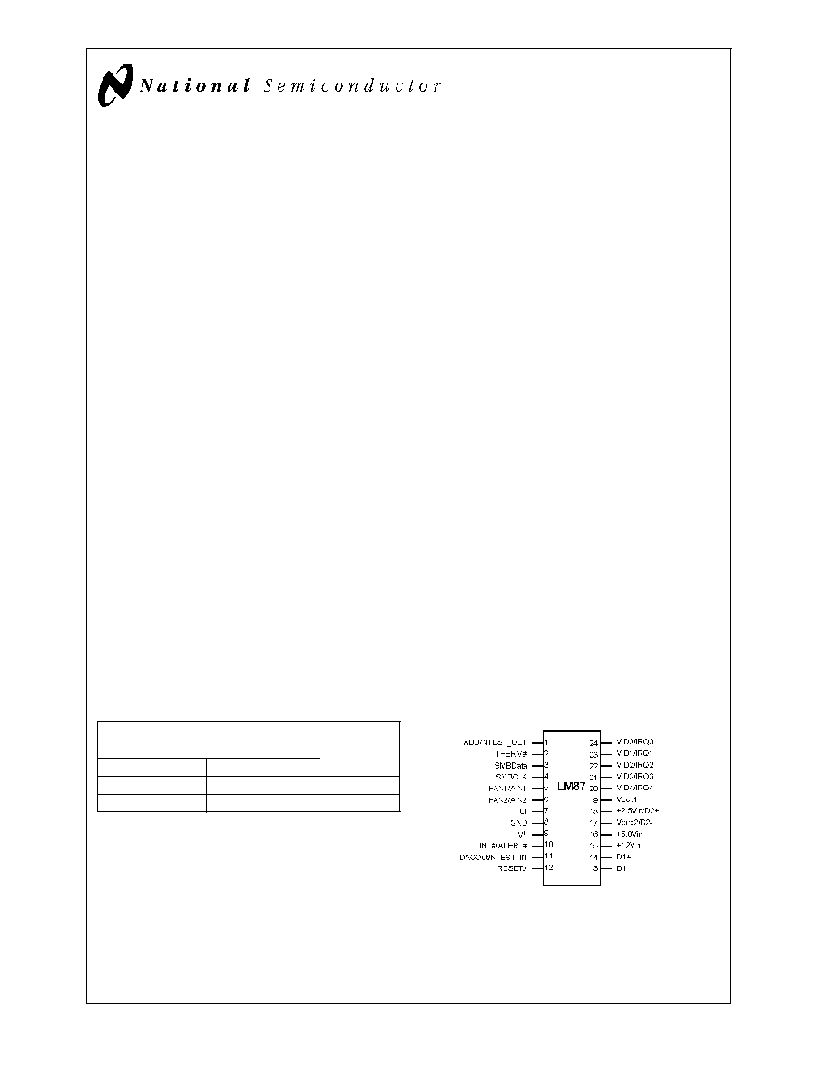
Connection Diagram
TRI-STATE
Æ
is a registered trademark of National Semiconductor Corporation.
WATCHDOG
TM
is a trademark of National Semiconductor Corporation.
SMBus
TM
is a trademark of the Intel Corporation.
DS100995-3
April 2000
LM87
Serial
Interface
System
Hardware
Monitor
with
Remote
Diode
T
emperature
Sensing
© 2000 National Semiconductor Corporation
DS100995
www.national.com
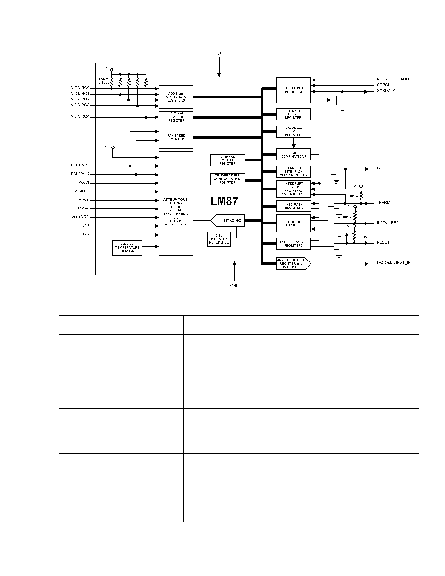
Block Diagram
Pin Description
Pin
Name(s)
Pin
Number
Number
of Pins
Type
Description
ADD/NTEST_OUT
1
1
Digital I/0
This pin normally functions as a three-state input that controls the
two LSBs of the Serial Bus Address. When this pin is tied to V
CC
the two LSBs are 01. When tied to Ground, the two LSBs are 10.
If this pin is not connected, the two LSBs are 00. This pin also
functions as an output during NAND Tree tests (board-level
connectivity testing). To ensure proper NAND tree function, this
pin should not be tied directly to V
CC
or Ground. Instead, a series
5 k
resistor should be used to allow the test output function to
work. Refer to
SECTION 11 on NAND Tree testing.
THERM#
2
1
Digital I/O
This pin functions as an open-drain interrupt output for
temperature interrupts only, or as an interrupt input for fan control.
It has an on-chip 100 k
pullup resistor.
SMBData
3
1
Digital I/O
Serial Bus bidirectional Data. Open-drain output.
SMBCLK
4
1
Digital Input
Serial Bus Clock.
FAN1/AIN1-
FAN2/AIN2
5-6
2
Analog/Digital
Inputs
Programmable as analog inputs (0 to 2.5V) or digital Schmitt
Trigger fan tachometer inputs.
CI
7
1
Digital I/O
An active high input from an external circuit which latches a
Chassis Intrusion event. This line can go high without any
clamping action regardless of the powered state of the LM87.
There is also an internal open-drain output on this line, controlled
by Bit 7 of the CI Clear Register (46h), to provide a minimum 20
ms reset pulse.
DS100995-1
LM87
www.national.com
2

Pin Description
(Continued)
Pin
Name(s)
Pin
Number
Number
of Pins
Type
Description
GND
8
1
GROUND
The system ground pin. Internally connected to all circuitry. The
ground reference for all analog inputs and the DAC output. This
pin needs to be connected to a low noise analog ground plane for
optimum performance of the DAC output.
V
+
(+2.8 V to
+3.8 V)
9
1
POWER
+3.3 V V
+
power. Bypass with the parallel combination of 10 µF
(electrolytic or tantalum) and 0.1 µF (ceramic) bypass capacitors.
INT# /ALERT#
10
1
Digital Output
Interrupt active low open-drain output. This output is enabled when
Bit 1 in the Configuration Register is set to 1. The default state is
disabled. It has an on-chip 100 k
pullup resistor. Alternately used
as an active low output to signal SMBus Alert Response Protocol.
DACOut/NTEST_IN
11
1
Analog
Output/Digital
Input
0 V to +2.5 V amplitude 8-bit DAC output. When forced high on
power up by an external voltage the NAND Tree Test mode is
enabled which provides board-level connectivity testing.
RESET#
12
1
Digital I/O
Master Reset, 5 mA driver (open-drain), active low output with a
45 ms minimum pulse width. Available when enabled via Bit 4 in
the Configuration register. It also acts as an active low power on
RESET input. It has an on-chip 100 k
pullup resistor.
D1-
13
1
Analog Input
Analog input for monitoring the cathode of the first external
temperature sensing diode.
D1+
14
1
Analog Input
Analog input for monitoring the anode of the first external
temperature sensing diode.
+12Vin
15
1
Analog Input
Analog input for monitoring +12 V.
+5Vin
16
1
Analog Input
Analog input for monitoring +5 V.
Vccp2/D2-
17
1
Analog Input
Digitally programmable analog input for monitoring Vccp2 (0 to 3.6
V input range) or the cathode of the second external temperature
sensing diode.
+2.5Vin/D2+
18
1
Analog Input
Digitally programmable analog input for monitoring +2.5 V or the
anode of the second external temperature sensing diode.
Vccp1
19
1
Analog Input
Analog input (0 to 3.6 V input range) for monitoring Vccp1, the
core voltage of processore 1.
VID4/IRQ4-
VID0/IRQ0
20-24
5
Digital Inputs
Digitally programmable dual function digital inputs. Can be
programmed to monitor the VID pins of the Pentium/PRO and
Pentium II processors, that indicate the operating voltage of the
processor, or as interrupt inputs. The values are read in the
VID/Fan Divisor Register and the VID4 Register. These inputs
have on-chip 100 k
pullup resistors.
TOTAL PINS
24
# Indicates Active Low ("Not")
LM87
www.national.com
3
Absolute Maximum Ratings
(Notes 1, 2)
If Military/Aerospace specified devices are required,
please contact the National Semiconductor Sales Office/
Distributors for availability and specifications.
Positive Supply Voltage (V
+
)
+6.0 V
Voltage on Any Input or Output Pin:
+12Vin
-0.3 V to +18 V
ADD/NTESTOUT,
DACOut/NTEST_IN, AIN1, AIN2
-0.3 V to
(V
+
+ 0.3 V)
All other pins
-0.3 V to +6 V
Input Current at any Pin (Note 4)
±
5 mA
Package Input Current (Note 4)
±
20 mA
Maximum Junction Temperature
(T
J
max)
150 ∞C
ESD Susceptibility (Note 6)
Human Body Model
2000 V
Soldering Information
MTC Package (Note 7) :
Vapor Phase (60 seconds)
215 ∞C
Infrared (15 seconds)
235 ∞C
Storage Temperature
-65 ∞C to +150 ∞C
Operating Ratings
(Notes 1, 2)
Operating Temperature Range
T
MIN
T
A
T
MAX
LM87
-55 ∞C
T
A
+125 ∞C
Specified Temperature Range
T
MIN
T
A
T
MAX
LM87
-40 ∞C
T
A
+125 ∞C
Junction to Ambient Thermal Resistance (
JA
(Note 5))
NS Package Number: MTC24B
95 ∞C/W
Supply Voltage (V
+
)
+2.8 V to +3.8 V
V
IN
Voltage Range:
+12Vin
-0.05 V to +15 V
+5Vin
-0.05 V to +6.8 V
+3.3Vin
-0.05 V to +4.6 V
+2.5Vin
-0.05 V to +3.6 V
VID0 - VID4, Vccp
-0.05 V to +6.0 V
All other inputs
-0.05 V to (V
+
+ 0.05 V)
DC Electrical Characteristics
The following specifications apply for +2.8 V
DC
V
+
+3.8 V
DC
, Analog voltage inputs R
S
= 510
, unless otherwise speci-
fied. Boldface limits apply for T
A
= T
J
= T
MIN
to T
MAX
; all other limits T
A
= T
J
= 25 ∞C.(Note 8)
Symbol
Parameter
Conditions
Typical
Limits
Units
(Note 9)
(Note 10)
(Limits)
POWER SUPPLY CHARACTERISTICS
I
+
Supply Current
Normal Mode, Interface
Inactive
0.7
2.0
mA (max)
Shutdown Mode
0.5
mA
TEMPERATURE-TO-DIGITAL CONVERTER CHARACTERISTICS
Temperature Error using Internal Diode
±
3
∞C
Temperature Error using Remote Pentium
Diode Sensor (Note 11) and (Note 12)
0 ∞C
T
A
+125 ∞C, Vcc
= 3.3 Vdc
±
3
∞C (max)
Temperature Error using Remote 2N3904
Sensor (Note 11) and (Note 12)
-40 ∞C
T
A
+125 ∞C,
Vcc = 3.3 Vdc
±
4
∞C (max)
Resolution
8 bits
1.0
∞C (min)
LM87 ANALOG-TO-DIGITAL CONVERTER CHARACTERISTICS
Resolution
8
bits
TUE
Total Unadjusted Error
(Note 13)
±
2
% (max)
DNL
Differential Non-Linearity
±
1
LSB (max)
t
C
Total Monitoring Cycle Time
(Note 14)
0.28
sec
ADC INPUT CHARACTERISTICS
Input Resistance (All analog inputs except
AIN1 and AIN2)
130
90
k
(min)
AIN1 and AIN2 DC Input Current
12
µA
LM87
www.national.com
4
DC Electrical Characteristics
(Continued)
The following specifications apply for +2.8 V
DC
V
+
+3.8 V
DC
, Analog voltage inputs R
S
= 510
, unless otherwise speci-
fied. Boldface limits apply for T
A
= T
J
= T
MIN
to T
MAX
; all other limits T
A
= T
J
= 25 ∞C.(Note 8)
Symbol
Parameter
Conditions
Typical
Limits
Units
(Note 9)
(Note 10)
(Limits)
DAC CHARACTERISTICS
Resolution
8
Bits
DAC Error
0 ∞C
T
A
+75 ∞C, V
+
=
3.3 V, Code = 255
±
3.3
% (max)
V
+
= 3.3 V, 3/4 Scale
+8
%
V
+
= 3.3 V, Code =
7(Note 15)
+4/-2.7
% (max)
R
L
Output Load Resistance
V
O
= 2.5 V
1250
(min)
C
L
Output Load Capacitance
20
pF (max)
FAN RPM-TO-DIGITAL CONVERTER
Fan RPM Error
+25 ∞C
T
A
+75 ∞C
±
10
% (max)
-10 ∞C
T
A
+100 ∞C
±
15
% (max)
-40 ∞C
T
A
+125 ∞C
±
20
% (max)
Full-scale Count
255
(max)
FAN1 and FAN2 Nominal Input
RPM (See
Section 6.0)
Divisor = 1, Fan Count =
153 (Note 16)
8800
RPM
Divisor = 2, Fan Count =
153 (Note 16)
4400
RPM
Divisor = 3, Fan Count =
153 (Note 16)
2200
RPM
Divisor = 4, Fan Count =
153 (Note 16)
1100
RPM
LM87
www.national.com
5
DC Electrical Characteristics
(Continued)
The following specifications apply for +2.8 V
DC
V
+
+3.8 V
DC
, Analog voltage inputs R
S
= 510
, unless otherwise speci-
fied. Boldface limits apply for T
A
= T
J
= T
MIN
to T
MAX
; all other limits T
A
= T
J
= 25 ∞C.(Note 8)
Symbol
Parameter
Conditions
Typical
Limits
Units
(Note 9)
(Note 10)
(Limits)
DIGITAL OUTPUTS (NTEST_OUT)
V
OUT(1)
Logical "1" Output Voltage
I
OUT
=
±
3.0 mA at
V
+
= +2.8 V
2.4
V (min)
V
OUT(0)
Logical "0" Output Voltage
I
OUT
=
±
3.0 mA at
V
+
= +3.8 V
0.4
V (max)
OPEN- DRAIN DIGITAL OUTPUTS (SMBData, RESET#, CI, INT#, THERM#)
V
OUT(0)
Logical "0" Output Voltage (SMBData)
I
OUT
= -755 µA
0.4
V (min)
V
OUT(0)
Logical "0" Output Voltage (Others)
I
OUT
= -3 mA
0.4
V (min)
I
OH
High Level Output Current
V
OUT
= V
+
5
12
µA (max)
RESET# and Chassis Intrusion
45
20
ms (min)
Pulse Width
DIGITAL INPUTS: VID0≠VID4, NTEST_IN, ADD/NTEST_OUT, Chassis Intrusion (CI)
V
IN(1)
Logical "1" Input Voltage
2.0
V (min)
V
IN(0)
Logical "0" Input Voltage
0.8
V (max)
SMBus DIGITAL INPUTS (SMBCLK, SMBData)
V
IN(1)
Logical "1" Input Voltage
2.1
V (min)
V
IN(0)
Logical "0" Input Voltage
0.8
V (max)
V
HYST
Input Hysteresis Voltage
243
mV
Tach Pulse Logic Inputs (FAN1, FAN2)
V
IN(1)
Logical "1" Input Voltage
0.7 x V
+
V (min)
V
IN(0)
Logical "0" Input Voltage
0.3 x V
+
V (max)
ALL DIGITAL INPUTS
I
IN(1)
Logical "1" Input Current
V
IN
= V
+
-12
µA (min)
I
IN(0)
Logical "0" Input Current
V
IN
= 0 V
DC
12
µA (max)
C
IN
Digital Input Capacitance
20
pF
LM87
www.national.com
6

AC Electrical Characteristics
The following specifications apply for +2.8 V
DC
V
+
+3.8 V
DC
on SMB-
CLK and SMBData, unless otherwise specified. Boldface limits apply for T
A
= T
J
= T
MIN
to T
MAX
; all other limits T
A
=
T
J
= 25∞C. (Note 17)
Symbol
Parameter
Conditions
Typical
Limits
Units
(Note 9)
(Note 10)
(Limits)
SERIAL BUS TIMING CHARACTERISTICS
t
1
SMBCLK (Clock) Period
2.5
µs (min)
t
rise
SMBCLK and SMBData Rise Time
1
µs (max)
t
fall
SMBCLK and SMBData Fall Time
300
ns (max)
t
2
Data In Setup Time to SMBCLK High
100
ns (min)
t
3
Data Out Stable After SMBCLK Low
100
ns (min)
300
ns (max)
t
4
SMBData Low Setup Time to SMBCLK Low
(start)
100
ns (min)
t
5
SMBData High Hold Time After SMBCLK
High (stop)
100
ns (min)
t
TIMEOUT
SMBData or SMBCLK low time required to
reset the Serial Bus Interface to the Idle
State
31
25
35
ms
ms (min)
ms (max)
C
L
Capacitive Load on SMBCLK and SMBData
80
pF (max)
DS100995-4
FIGURE 1. Serial Bus Timing Diagram
LM87
www.national.com
7
Electrical Characteristics (Continued)
Note 1: Absolute Maximum Ratings indicate limits beyond which damage to the device may occur. Operating Ratings indicate conditions for which the device is
functional, but do not guarantee specific performance limits. For guaranteed specifications and test conditions, see the Electrical Characteristics. The guaranteed
specifications apply only for the test conditions listed. Some performance characteristics may degrade when the device is not operated under the listed test condi-
tions.
Note 2: All voltages are measured with respect to GND, unless otherwise specified.
Note 3: The Absolute maximum input range for :
+2.5Vin - -0.3 V to (1.4 x V
+
+ 0.42 V or 6 V, whichever is smaller
+3.3Vin - -0.3 V to (1.8 x V
+
+ 0.55 V or 6 V, whichever is smaller.
Note 4: When the input voltage (V
IN
) at any pin exceeds the power supplies (V
IN
<
GND or V
IN
>
V
+
), the current at that pin should be limited to 5 mA. The 20 mA
maximum package input current rating limits the number of pins that can safely exceed the power supplies with an input current of 5 mA to four.
Note 5: The maximum power dissipation must be derated at elevated temperatures and is dictated by T
J
max,
JA
and the ambient temperature, T
A
. The maximum
allowable power dissipation at any temperature is P
D
= (T
J
max-T
A
)/
JA
.
Note 6: The human body model is a 100 pF capacitor discharged through a 1.5 k
resistor into each pin.
Note 7: See the section titled "Surface Mount" found in any post 1986 National Semiconductor Linear Data Book for other methods of soldering surface mount de-
vices.
Note 8: Parasitics and or ESD protection circuitry are shown in the figure below for the LM87's pins. The nominal breakdown voltage of the zener D3 is 6.5 V. Care
should be taken not to forward bias the parasitic diode, D1, present on pins: A0/NTEST_OUT, A1 and DACOut/NTEST_IN. Doing so by more than 50 mV may corrupt
a temperature or voltage measurement.
Pin Name
D1
D2
D3
R1
R2
R3
R4
Pin Name
D1
D2
D3
R1
R2
R3
R4
INT#
x
x
x
0
100k
1M
+12Vin
x
x
R1+R2
130k
CI
x
x
x
0
1M
+5Vin
x
x
R1+R2
130k
FAN1≠FAN2
x
x
x
0
1M
+3.3Vin, +2.5Vin,
Vccp1, Vccp2
x
x
x
R1+R2
130k
1M
SMBCLK
x
x
x
0
1M
THERM
x
x
x
0
100k
1M
SMBData
x
x
x
0
1M
VID4≠VID0
x
x
x
0
100k
1M
RESET#
x
x
x
0
100k
1M
DACOut/NTEST_IN
x
x
x
0
1M
ADD/NTEST_OUT
x
x
x
0
1M
Note 9: Typicals are at T
J
= T
A
= 25 ∞C and represent most likely parametric norm.
Note 10: Limits are guaranteed to National's AOQL (Average Outgoing Quality Level).
Note 11: The Temperature Error specification does not include an additional error of
±
1∞C, caused by the quantization error.
Note 12: The Temperature Error will vary less than
±
1∞C over the operating Vcc range of 2.8V to 3.8V.
Note 13: TUE (Total Unadjusted Error) includes Offset, Gain and Linearity errors of the ADC.
Note 14: Total Monitoring Cycle Time includes all diode checks, temperature conversions and analog input voltage conversions. Fan tachometer readings are de-
termined separately and do not affect the completion of the monitoring cycle.
Note 15: This is the lowest DAC code guaranteed to give a non-zero DAC output.
Note 16: The total fan count is based on 2 pulses per revolution of the fan tachometer output.
Note 17: Timing specifications are tested at the specified logic levels, V
IL
for a falling edge and V
IH
for a rising edge.
DS100995-5
An x indicates that the diode exists.
FIGURE 2. ESD Protection Input Structure
LM87
www.national.com
8
Test Circuit
Functional Description
1.0 GENERAL DESCRIPTION
The LM87 provides 7 analog inputs, an internal junction type
temperature sensor, two remote junction temperature sens-
ing channels, a Delta-Sigma ADC (Analog-to-Digital Con-
verter), a DAC output, 2 fan speed counters, WATCHDOG
registers, and a variety of inputs and outputs on a single
chip. A two wire SMBus Serial Bus interface is included. The
LM87 performs power supply, temperature, fan control and
fan monitoring for personal computers.
The analog inputs are useful for monitoring several power
supplies present in a typical computer. The LM87 includes
internal resistor dividers that scale external Vccp1, Vccp2,
+2.5V, +5.0 V, +12 V and internal +3.3V power supply volt-
ages to a 3/4 scale nominal ADC output. Two additional in-
puts, +AIN1 and +AIN2 (2.5V full scale) are input directly
with no resistive dividers. The LM87 ADC continuously con-
verts the scaled inputs to 8-bit digital words. Measurement of
negative voltages (such as -5 V and -12 V power supplies)
can be accommodated with an external resistor divider ap-
plied to the +AIN1 or +AIN2 inputs. Internal and external
temperature is converted to 8-bit two's-complement digital
words with a 1 ∞C LSB.
Fan inputs measure the period of tachometer pulses from
the fans, providing a higher count for lower fan speeds. The
fan inputs are Schmitt-Trigger digital inputs with an accept-
able range of 0 V to V
+
and a transition level of approxi-
mately V
+
/2. Full scale fan counts are 255 (8-bit counter) and
this represents a stopped or very slow fan. Nominal speeds,
based on a count of 153, are programmable from 1100 to
8800 RPM on FAN1 and FAN2. Schmitt-Trigger input cir-
cuitry is included to accommodate slow rise and fall times.
An 8 bit DAC with 0 V to 2.5 V output voltage range can be
used for control of fan speed.
The LM87 has several internal registers, as shown in
Figure
4, Table 1 and Section 13.0. These include:
∑
Configuration Registers:
Provide control and con-
figuration.
∑
Channel Mode Register:
Controls the functionality of
the dual purpose input pins, scaling for internal Vcc mea-
surement, and operation of IRQ inputs.
∑
Interrupt Status Registers:
Two registers to provide
status of each WATCHDOG limit or Interrupt event.
Reading the Status Registers clears any active bits.
∑
Interrupt Status Mirror Registers:
Two registers to
provide status of each WATCHDOG limit or Interrupt
event. Reading the Mirror Registers does not affect the
status bits.
∑
Interrupt Mask Registers:
Allows masking of indi-
vidual Interrupt sources, as well as separate masking for
each of the two hardware Interrupt outputs.
∑
CI Clear Register:
Allows transmitting a 20 ms low
pulse on the chassis intrusion pin (CI).
∑
VID/Fan Divisor Register:
This register contains the
state of the VID0-VID3 input lines and the divisor bits for
FAN1 and FAN2 inputs.
∑
VID4 Register:
Contains the state of the VID4 input.
∑
Extended Mode Register:
Enable and control the
Alert Response operation.
∑
Hardware High Limit Registers:
Registers at 13h,
14h, 17h and 18h where Internal and External 'Hardware'
WATCHDOG temperature high limits are stored. These
limits have Power On Default settings but can be ad-
justed by the user. The values stored at 13h and 14h can
be locked down by setting bits 1 and 2 of Configuration
Register 2.
DS100995-6
FIGURE 3. Digital Output Load Test Circuitry
LM87
www.national.com
9
Functional Description
(Continued)
∑
Value and Limit RAM:
The DAC digital output, moni-
toring
results
(temperature,
voltages,
fan
counts),
WATCHDOG limits, and Company/Stepping IDs are all
contained in the Value RAM. The Value RAM consists of
a total of 33 bytes, addresses 19h - 3Fh, containing:
-- byte 1 at address 19h contains the DAC Data Regis-
ter
-- locations 1Ah and 1Bh contain the WATCHDOG low
limits for AIN1 and AIN2
-- locations 1Ch - 1Fh are unassigned and do not have
associated registers
-- the next 10 bytes at addresses 20h -29h contain all of
the results
-- location 2Ah is unassigned and does not have an as-
sociated register
-- the next 18 bytes at addresses 2Bh-3Ch are the re-
maining WATCHDOG limits
-- the last 2 bytes at addresses 3Eh and 3Fh contain the
Company ID and Stepping ID numbers, respectively
When the LM87 is started, it cycles through each measure-
ment in sequence, and it continuously loops through the se-
quence approximately once every 0.4 s. Each measured
value is compared to values stored in WATCHDOG, or Hard-
ware High Limit registers. When the measured value violates
the programmed limit the LM87 will set a corresponding In-
terrupt in the Interrupt Status Registers. The hardware Inter-
rupt line INT# is fully programmable with separate masking
of each Interrupt source. In addition, the Configuration Reg-
ister has a control bit to enable or disable the hardware Inter-
rupt. Another hardware Interrupt line available, THERM# is
used to signal temperature specific events. Having a dedi-
cated interrupt for these conditions allows specific actions to
be taken for thermal events. This output is enabled by setting
bit 2 of Configuration Register 1.
The Chassis Intrusion input is designed to accept an active
high signal from an external circuit that activates and latches
when the case is removed from the computer.
2.0 INTERFACE
DS100995-7
FIGURE 4. LM87 Register Structure
LM87
www.national.com
10

Functional Description
(Continued)
2.1 Internal Registers of the LM87
TABLE 1. The internal registers and their corresponding internal LM87 addresses are as follows:
Register
LM87 Internal Hex
Address
Power on
Value
Notes
Internal Temp. Hardware
High Limit
13h
0100 0110
70 ∞C Default - User adjustable. Lockable by setting
bit 1 of register 4Ah.
External Temp. Hardware
High Limit
14h
0101 0101
85 ∞C Default - User adjustable. Lockable by setting
bit 2 of register 4Ah.
Test Register
15h
0000 0000
Channel Mode Register
16h
0000 0000
Internal Temp. Hardware
High Limit
17h
0100 0110
70 ∞C Default - User adjustable.
External Temp. Hardware
High Limit
18h
0101 0101
85 ∞C Default - User adjustable.
Value RAM DAC Data
Register
19h
1111 1111
Defaults to full scale DAC setting.
Value RAM
20h-3Fh
Contains: monitoring results (temperature, voltages,
fan counts), WATCHDOG limits, and
Company/Stepping IDs
Company ID
3Eh
0000 0010
This designates the National Semiconductor LM87.
Revision
3Fh
0000 0100
Revisions of this device will start with 1 and
increment by one.
Configuration Register 1
40h
0000 1000
Interrupt Status Register 1
41h
0000 0000
Interrupt Status Register 2
42h
0000 0000
Interrupt Mask Register 1
43h
0000 0000
Interrupt Mask Register 2
44h
0000 0000
CI Clear Register
46h
0000 0000
VID0-3/Fan Divisor Register
47h
0101 XXXX
The upper four bits set the divisor for Fan Counters 1
and 2. The lower four bits reflect the state of the
VID0-VID3 inputs.
VID4 Register
49h
1000 000X
The lower bit reflects the state of VID4 input.
Configuration Register 2
4Ah
0000 0000
Interrupt Status Register 1
Mirror
4Ch
0000 0000
Interrupt Status Register 2
Mirror
4Dh
0000 0000
SMBALERT# Enable
80h
0010 0000
LM87
www.national.com
11
Functional Description
(Continued)
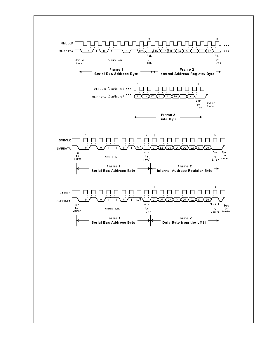
2.2 Serial Bus Interface
The Serial Bus control lines consist of the SMBData (serial
data), SMBCLK (serial clock) and ADD (address) pin. The
LM87 can operate only as a slave. The SMBCLK line only
controls the serial interface, all other clock functions within
LM87 such as the ADC and fan counters are done with a
separate asynchronous internal clock.
When using the Serial Bus Interface, a write will always con-
sist of the LM87 Serial Bus Interface Address byte, followed
by the Internal Address Register byte, then the data byte.
There are two cases for a read:
1.
If the Internal Address Register is known to already be at
the desired Address, simply read the LM87 with the Se-
rial Bus Interface Address byte, followed by the data
byte read from the LM87.
2.
If the Internal Address Register value is unknown, or if it
is not the desired value, write to the LM87 with the Serial
Bus Interface Address byte, followed by the Internal Ad-
dress Register byte. Then restart the Serial Communica-
tion with a Read consisting of the Serial Bus Interface
Address byte, followed by the data byte read from the
LM87.
The Serial Bus address of the LM87 is set to 010 11(X)(Y).
All bits, except for X and Y, are fixed and cannot be changed.
The values for X and Y are set by the state of the ADD pin on
power up. If ADD is tied to ground the value for XY is 10. If
ADD is tied to Vcc XY will be set to 01. If ADD is not con-
nected, XY will be 00. XY = 11 is not a possible combination.
All of these communications are depicted in the Serial Bus
Interface Timing Diagrams as shown in
Figure 5. The ex-
ample shown corresponds to the ADD pin tied to Vcc, so
XY=01 and the resulting LM87 address is 0101101.
DS100995-8
(a) Serial Bus Write to the Internal Address Register followed by the Data Byte
DS100995-9
(b) Serial Bus Write to the Internal Address Register Only
DS100995-10
(c) Serial Bus Read from a Register with the Internal Address Register Preset to Desired Location
FIGURE 5. Serial Bus Timing
LM87
www.national.com
12

Functional Description
(Continued)
Serial Bus Timeout can be initiated by holding the SMBCLK
line low for greater than t
TIMEOUT
(35 ms max). Serial Bus
Timeout resets the serial bus interface circuitry to the idle
state and readies the LM87 for a new serial bus communica-
tion.
3.0 USING THE LM87
3.1 Power On
When power is first applied, the LM87 performs a "power on
reset" on several of its registers. The power on condition of
the LM87's registers is shown in
Table 1 Registers whose
power on values are not shown have power on conditions
that are indeterminate (this includes the value RAM ,exclu-
sive of the DAC data, and WATCHDOG limits). When power
is first applied the ADC is inactive. In most applications, the
first action after power on is to write WATCHDOG limits into
the Value RAM.
3.2 Resets
All register values, except the Programmed DAC Output can
be returned to their
power on
default values by taking the
RESET# input low for at least TBD ns or by performing a
Configuration Register INITIALIZATION. The Value RAM
conversion results, and Value RAM WATCHDOG limits are
not Reset and will be indeterminate immediately after power
on. If the Value RAM contains valid conversion results and/or
Value RAM WATCHDOG limits have been previously set,
they will not be affected by a Configuration Register INITIAL-
IZATION. The Power On Reset, RESET# input, and Configu-
ration Register INITIALIZATION, clear or initialize the follow-
ing registers (the initialized values are shown on Table I).
Power On Reset also sets the Programmed DAC Output to
full scale (FFh) Hardware High Limit registers 13h, and 14h
will only be returned to default values if the
Write Once
bits
in Configuration Register 2 have not been set:
∑
Configuration Registers 1 and 2
∑
Channel Mode Register
∑
Hardware High Limit Registers
∑
Interrupt Status Register 1
∑
Interrupt Status Register 2
∑
Interrupt Status Mirror Register 1
∑
Interrupt Status Mirror Register 2
∑
Interrupt Mask Register 1
∑
Interrupt Mask Register 2
∑
Chassis Intrusion Clear Register
∑
VID/Fan Divisor Register
∑
VID4 Register
∑
Extended Mode Register
Configuration Register INITIALIZATION is accomplished by
setting Bit 7 of Configuration Register 1 high. This bit auto-
matically clears after being set.
3.3 Configuration Registers and Channel Mode
Register
The Configuration Registers and Channel Mode Register
control the LM87 operation. At power on, the ADC is stopped
and INT_Clear is asserted, clearing the INT# hardwire out-
put. These registers start and stop the LM87, enable and dis-
able interrupt output, configure the operation of dual function
inputs, and provide the Reset functions described in
Section
3.2.
Bit 0 of Configuration Register 1 controls the monitoring loop
of the LM87. Setting Bit 0 low stops the LM87 monitoring
loop and puts the LM87 in shutdown mode, reducing power
consumption. Serial Bus communication can take place with
any register in the LM87 although activity on the SMBData
and SMBCLK lines will increase shutdown current, up to as
much as maximum rated supply current, while the activity
takes place. Taking Bit 0 high starts the monitoring loop, de-
scribed in more detail subsequently.
Bit 1 of Configuration Register 1 enables the INT# Interrupt
output when this bit is taken high.
Bit 2 of Configuration Register 1 enables the THERM# Inter-
rupt output when this bit is taken high.
Bit 3 of Configuration Register 1 clears the INT# output when
set high, without affecting the contents of the Interrupt Status
Registers. The LM87 will stop monitoring. It will resume upon
clearing of this bit.
Bit 4 of Configuration Register 1 provides an active low 45
ms pulse at the RESET# output when set high.
Bit 6 of Configuration Register 1 clears the THERM# output
when set high, without affecting the contents of the Interrupt
Status Registers.
Bit 7 of Configuration Register 1 (the INITIALIZATION bit) re-
sets the internal registers of the LM87 as described in
Sec-
tion 3.2.
Bit 7 of the CI_Clear Register provides an active low 20 ms
pulse at the CI# output pin when set high. This is intended
for resetting the Chassis Intrusion circuitry.
Bit 0 of Configuration Register 2 enables the INT# Interrupt
output for THERM# events when set low. When this bit is set
high, THERM# error events will not affect the INT# output.
Bit 1 of Configuration Register 2 locks the value set in the In-
ternal Temperature high limit register at 13h. The value can-
not be changed until a Power On Reset is performed.
Bit 2 of Configuration Register 2 locks the value set in the
External Temperature high limit register at 14h. The value
cannot be changed until a Power On Reset is performed.
Bit 3 of Configuration Register 2 sets the THERM# output
mode. When set to 0, the THERM# output functions in de-
fault mode, when set to 1, THERM# operates in ACPI mode.
Bit 6 of Configuration Register 2, when set to 1, enables pin
21 as an active high (IRQ3) interrupt input. When set to 0,
this input is disabled as an IRQ interrupt.
Bit 7 of Configuration Register 2, when set to 1, enables pin
20 as an active high (IRQ4) interrupt input. When set to 0,
this input is disabled as an IRQ interrupt.
Bit 0 of the Channel Mode Register, when set to 1, config-
ures pin 5 as AIN1. When set to 0, pin 5 is configured as the
FAN1 input.
Bit 1 of the Channel Mode Register, when set to 1, config-
ures pin 6 as AIN2. When set to 0, pin 6 is configured as the
FAN2 input.
Bit 2 of the Channel Mode Register, when set to 0, config-
ures pins 18 and 19 as +2.5V and V
CCP2
voltage inputs.
When set to 1, pins 18 and 19 are configured as a second re-
mote temperature sensing channel.
Bit 3 of the Channel Mode Register, when set to 0, sets the
nominal voltage for internal V
CC
measurement to 3.3V.
When set to 1, the nominal V
CC
range is 5V.
LM87
www.national.com
13
Functional Description
(Continued)
Bit 4 of the Channel Mode Register, when set to 1, enables
pin 24 as an active low (IRQ0) interrupt input. When set to 0,
this input is disabled as an IRQ interrupt.
Bit 5 of the Channel Mode Register, when set to 1, enables
pin 23 as an active low (IRQ1) interrupt input. When set to 0,
this input is disabled as an IRQ interrupt.
Bit 6 of the Channel Mode Register, when set to 1, enables
pin 22 as an active low (IRQ2) interrupt input. When set to 0,
this input is disabled as an IRQ interrupt.
Bit 7 of the Channel Mode Register, when set to 1, config-
ures pins 20 to 24 as interrupt inputs. When set to 0, pins 20
to 24 are configured as processor voltage ID pins.
3.4 Starting Conversions
The monitoring function (Analog inputs, temperature, and
fan speeds) in the LM87 is started by writing to Configuration
Register 1 and setting INT_Clear (Bit 3) low, and Start (bit 0)
high. The LM87 then performs a "round-robin" monitoring of
all analog inputs, temperature, and fan speed inputs approxi-
mately once every 0.3 s. The sequence of items being moni-
tored is:
1.
Check D1 connections
2.
Check D2 connections
3.
Internal Temperature
4.
External D1 Temperature
5.
External D2 Temperature
6.
+2.5V
7.
+Vccp1
8.
Vcc 3.3V
9.
Vcc 5.0V
10. +5Vin
11. +12Vin
12. +Vccp2
13. AIN1
14. AIN2
15. Fan 1
16. Fan 2
DACOut immediately changes after the DAC Data Register
in the Value RAM has been updated. For a zero to full scale
transition DACOut will typically settle within 100 µsec of the
stop by master in the write to the DAC Data Register Serial
Bus transaction. The DAC Data Register is not reset by the
INITIALIZATION bit found in the Configuration Register.
3.5 Reading Conversion Results
The conversion results are available in the Value RAM. Con-
versions can be read at any time and will provide the result
of the last conversion. Because the ADC stops, and starts a
new conversion whenever it is read, reads of any single
value should not be done more often than once every 56 ms.
When reading all values, allow at least 0.6 seconds between
reading groups of values. Reading more frequently than
once every 0.6 seconds can also prevent complete updates
of Interrupt Status Registers and Interrupt Output's.
A typical sequence of events upon power on of the LM87
would consist of:
1.
Set WATCHDOG Limits
2.
Set Interrupt Masks
3.
Start the LM87 monitoring process
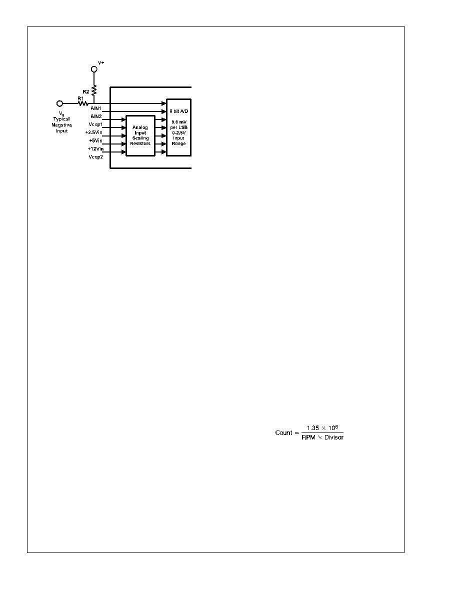
4.0 ANALOG INPUTS
All analog input voltages are digitized to 8-bits of resolution.
For safety purposes, and to provide maximum accuracy, a
510
resistor should be placed in series with all analog volt-
age inputs. The resistors will limit the possible current drawn
from the power supplies in the event that circuit board traces
are bridged, or accidentally shorted during test. All analog in-
puts, except for AIN1 and AIN2, include internal resistor at-
tenuators. The theoretical LSB size, theoretical voltage input
required for an ADC reading of 192 (3/4 scale) and 255 (full
scale) for each analog input is detailed in the table below:
Input
LSB size
Vin for
192
Vin for
255
2.5Vin
13 mV
2.5 V
3.320 V
3.3Vcc
17.2 mV
3.3 V
4.383 V
5Vin/Vcc
26 mV
5 V
6.641 V
12Vin
62.5 mV
12 V
15.93 V
Vccp1, Vccp2
14.1 mV
2.7 V
3.586 V
AIN1/AIN2
9.8 mV
1.875 V
2.49 V
Thus monitoring power supplies within a system can be eas-
ily accomplished by tying the Vccp, +2.5Vin, +5Vin and
+12Vin analog inputs to the corresponding system supply.
Vcc of the LM87 will also be monitored. A digital reading can
be converted to a voltage by simply multiplying the decimal
value of the reading by the LSB size.
For inputs with attenuators the input impedance is greater
than 90 k
. AIN inputs do not have resistor attenuators and
are directly tied to the ADC, therefore having a much larger
input impedance.
A negative power supply voltage can be applied to a AIN in-
put through a resistor divider referenced to a known positive
DC voltage as shown in
Figure 6. The resistor values shown
in the table below for the circuit of
Figure 6 will provide ap-
proximately 1.25 V at the AIN analog inputs of the LM87 for
a nominal reading of 128.
Voltage
Measure-
ments
(V
S
)
R2
R1
V
+
Voltage
at
Analog In-
puts
( ADC code
128)
-12V
20 k
130 k
+3.3 V
+1.25 V
-5V
20 k
61.0
k
+3.3 V
+1.25 V
LM87
www.national.com
14
Functional Description
(Continued)
The resistors were selected by setting R2 = 20 k
and then
calculating R1 using the following equation, ( V
S
is the maxi-
mum negative input voltage, V
+
is the positive pullup volt-
age):
R1 = [(1.25V - V
S
) ˜ (V
+
- 1.25V)] x 20 k
The maximum R1 can be is restricted by the DC input cur-
rent of an AIN input.
Inputs with internal resistor dividers (+2.5Vin, +3.3Vin or
+5Vin, +12Vin) can have voltage applied that exceeds the
power supply up to: 3.6 V for +2.5Vin, 4.6 V for +3.3Vin, 6.8
V for +5Vin, and 15 V for +12Vin. The AIN inputs have a
parasitic diode to the positive supply, so care should be
taken not to forward bias this diode. All analog inputs have
internal diodes that clamp the input voltage when going be-
low ground thus limiting the negative analog input voltage
range to -50 mV. Violating the analog input voltage range of
any analog input has no detrimental effect on the other ana-
log inputs. External resistors should be included to limit input
currents to the values given in the ABSOLUTE MAXIMUM
RATINGS for Input Current At Any Pin whenever exceeding
the analog input voltage range, even on an un-powered
LM87. Inputs with external attenuator networks will usually
meet these requirements. If it is possible for inputs without
attenuators (such as AIN1 and AIN2) to be turned on while
LM87 is powered off, additional resistors of about 10 k
should be added in series with the inputs to limit the input
current.
4.1 Analog Input Interrupts
A WATCHDOG window comparison on the analog inputs
can activate the INT# interrupt output. A converted input volt-
age that is above its respective HIGH limit or less than or
equal to its LOW limit will cause a flag to be set in its Inter-
rupt Status Register. This flag will activate the INT# output
when its mask bit is set low. Mask bits are found in the Inter-
rupt Mask Registers.
5.0 LAYOUT AND GROUNDING
A separate, low-impedance ground plane for analog ground,
which provides a ground point for the GND pin, voltage divid-
ers and other analog components, will provide best perfor-
mance, but is not mandatory. Analog components such as
voltage dividers should be located physically as close as
possible to the LM87.
The power supply bypass, the parallel combination of 10 µF
(electrolytic or tantalum) and 0.1 µF (ceramic) bypass ca-
pacitors connected between pin 9 and ground, should also
be located as close as possible to the LM87.
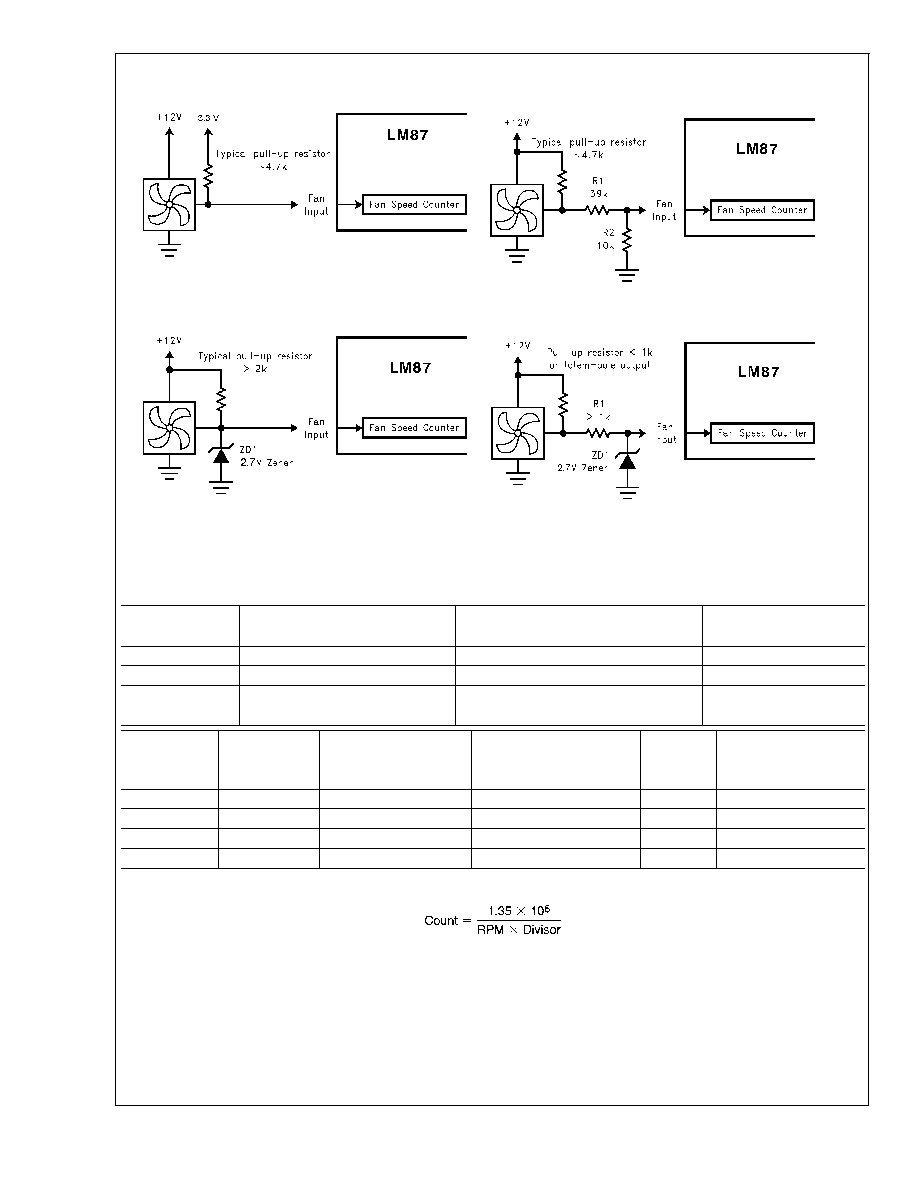
6.0 FAN INPUTS
The FAN1 and FAN2 inputs accept signals from fans
equipped with tachometer outputs. These are logic-level in-
puts with an approximate threshold of V
+
/2. Signal condition-
ing in the LM87 accommodates the slow rise and fall times
typical of fan tachometer outputs. The maximum input signal
range is 0 to V
+
. In the event these inputs are supplied from
fan outputs which exceed 0 to V
+
, either resistive division or
diode clamping must be included to keep inputs within an ac-
ceptable range, as shown in
Figure 7. R2 is selected so that
it does not develop excessive voltage due to input leakage.
R1 is selected based on R2 to provide a minimum input of
2 V and a maximum of V
+
. R1 should be as low as possible
to provide the maximum possible input up to V
+
for best
noise immunity. Alternatively, use a shunt reference or zener
diode to clamp the input level.
If fans can be powered while the power to the LM87 is off,
the LM87 inputs will provide diode clamping. Limit input cur-
rent to the Input Current at Any Pin specification shown in the
ABSOLUTE MAXIMUM RATINGS section. In most cases,
open collector outputs with pull-up resistors inherently limit
this current. If this maximum current could be exceeded, ei-
ther a larger pull up resistor should be used or resistors con-
nected in series with the fan inputs.
The Fan Inputs gate an internal 22.5 kHz oscillator for one
period of the Fan signal into an 8-bit counter (maximum
count = 255). The default divisor, located in the VID/Fan Di-
visor Register, is set to 2 (choices are 1, 2, 4, and 8) provid-
ing a nominal count of 153 for a 4400 rpm fan with two
pulses per revolution. Typical practice is to consider 70% of
normal RPM a fan failure, at which point the count will be
219.
Determine the fan count according to:
Note that Fan 1 and Fan 2 Divisors are programmable via
the VID/Fan Divisor Register.
Fan tachometer outputs that provide one pulse per revolu-
tion should use a divisor setting twice that of outputs that
provide two pulses per revolution. For example, a 4400 RPM
fan that provides one pulse per revolution should have the
divisor set to 4 such that the nominal counter output is 153.
DS100995-30
FIGURE 6. Input Examples. Resistor values shown in
table provide approximately 1.25V at the Vccp inputs.
LM87
www.national.com
15
Functional Description
(Continued)
Counts are based on 2 pulses per revolution tachometer outputs.
RPM
Time per Revolution
Counts for "Divide by 2"
Comments
(Default) in Decimal
4400
13.64 ms
153 counts
Typical RPM
3080
19.48 ms
219 counts
70% RPM
2640
22.73 ms
255 counts
60% RPM
(maximum counts)
Mode Select
Nominal
RPM
Time per Revolution
Counts for the
70%
RPM
Time per Revolution
Given Speed in Decimal
for 70% RPM
Divide by 1
8800
6.82 ms
153
6160
9.74 ms
Divide by 2
4400
13.64 ms
153
3080
19.48 ms
Divide by 4
2200
27.27 ms
153
1540
38.96 ms
Divide by 8
1100
54.54 ms
153
770
77.92 ms
7.0 DAC OUTPUT
The LM87 provides an 8-bit DAC (Digital-to-Analog Con-
verter) with an output range of 0 to 2.5 volts (9.80 mV LSB).
This DAC can be used in any way, but in most applications of
the LM87 the DAC will be used for fan control. Typically the
DAC output would be amplified to provide the up to 12 volt
drive required by the fan. At power-on the DAC provides full
output, insuring that full fan speed is the default condition.
Care should be taken such that the analog circuitry tied to
this pin does not drive this pin above 2.5 V. Doing so will
place the LM87 in NAND tree test mode which will make all
pins inputs. After the first SMBus communication with the
LM87, it will leave NAND tree test mode and all inputs/
outputs will function normally.
Fans do not start reliably at reduced voltages, so operation
at a reduced voltage should be preceded by a brief (typically
1 second) excursion to full operating voltage, then reduce
the voltage. Most fans do not operate at all below 5 to 7
DS100995-12
(a) Fan with Tach Pull-Up to +5V
DS100995-13
(b) Fan with Tach Pull-Up to +12V, or Totem-Pole
Output and Resistor Attenuator
DS100995-14
(c) Fan with Tach Pull-Up to +12V and Diode Clamp
DS100995-15
(d) Fan with Strong Tach Pull-Up or Totem Pole Output
and Diode Clamp
FIGURE 7. Alternatives for Fan Inputs
LM87
www.national.com
16
Functional Description
(Continued)
volts. At those lower voltages the fan will simply consume
current, dissipate power, and not operate, and such condi-
tions should be avoided.
The output of the amplifier can be configured to provide a
high or low side pass transistor. A high side pass transistor
simplifies the coupling of tachometer outputs to the tachom-
eter inputs of the LM87 since the fan remains grounded. Low
side drive will require AC coupling along with clamping at the
LM87 input to prevent negative excursions.
A typical circuit for fan drive is shown in
Figure 13.
8.0 TEMPERATURE MEASUREMENT SYSTEM
The LM87 temperature sensor(s) and ADC produce 8-bit
two's-complement temperature data. One internal diode
junction temperature, and up to two external junction tem-
peratures can be monitored. A digital comparator compares
the temperature data to the user-programmable High, Low,
and Hardware Limit setpoints, and Hysteresis values.
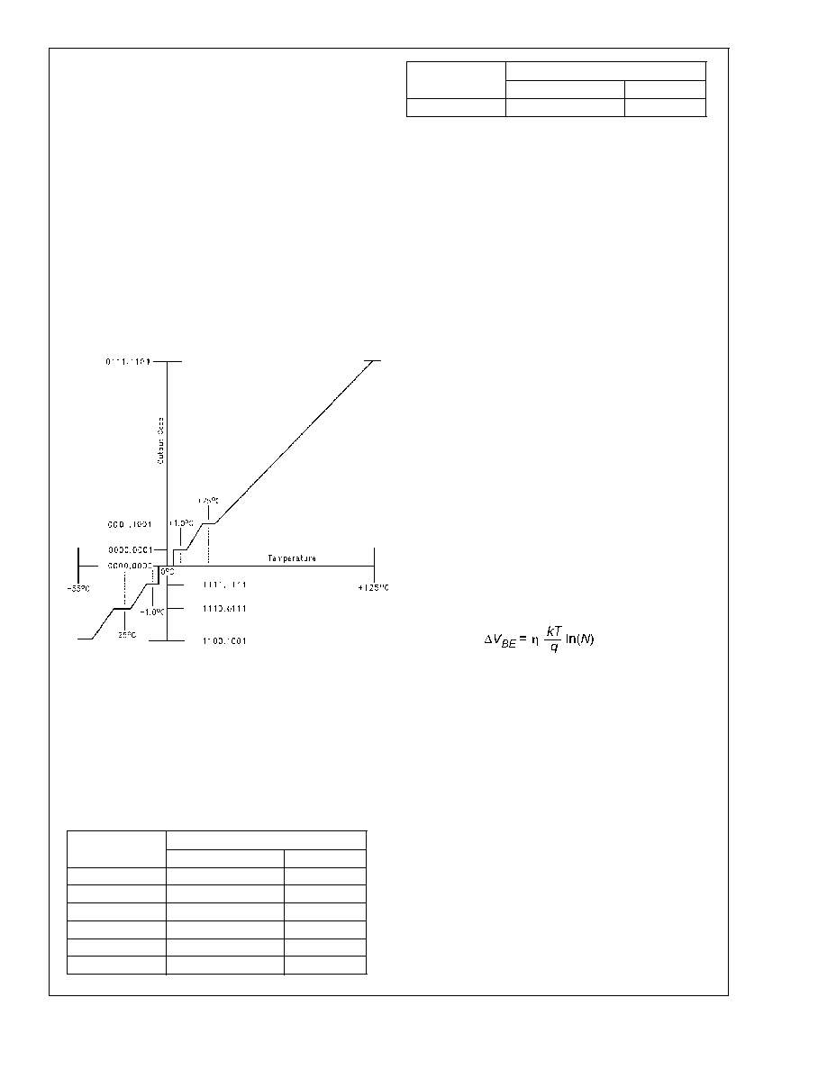
8.1 Temperature Data Format
Temperature data can be read from the Temperature, T
HIGH
setpoint, T
LOW
setpoint, and Hardware Temperature limit
registers; and written to the T
HIGH
setpoint, T
LOW
setpoint,
and Hardware Temperature limit registers. T
HIGH
setpoint,
T
LOW
setpoint, Hardware Temperature Limit, and Tempera-
ture data is represented by an 8-bit, two's complement word
with an LSB (Least Significant Bit) equal to 1∞C:
Temperature
Digital Output
Binary
Hex
+125∞C
0111 1101
7Dh
+25∞C
0001 1001
19h
+1.0∞C
0000 0001
01h
+0∞C
0000 0000
00h
-1.0∞C
1111 1111
FFh
-25∞C
1110 0111
E7h
Temperature
Digital Output
Binary
Hex
-55∞C
1100 1001
C9h
8.2 Internal Temperature Measurement
The LM87 internal temperature is monitored using a junction
type temperature sensor.
8.3 Remote Temperature Measurement
The LM87 monitors the temperature of remote semiconduc-
tor devices using the p-n junction temperature sensing prin-
cipal. Up to two remote IC, diode or bipolar transistor tem-
peratures can be monitored. The remote measurement
channels have been optimized to measure the remote diode
of a Pentium II processor. A discrete diode or bipolar transis-
tor can also be used to sense the temperature of external ob-
jects or ambient air. The 2N3904 NPN transistor base emit-
ter junction performs well in this type of application. When
using a 2N3904, the collector should be connected to the
base to provide a device that closely approximates the char-
acteristics of the Pentium II PNP monitoring diode.
When using two external 2N3904 sensors, the D- inputs
should be connected together. This provides the best pos-
sible accuracy by compensating for differences between the
2N3904 and Pentium II sensors.
During each conversion cycle, the remote monitoring inputs
perform an external diode fault detection sequence. If the D+
input is shorted to V
CC
or floating then the temperature read-
ing will be +127∞C, and bit 6 or bit 7 of Interrupt Status Reg-
ister 2 will be set. If D+ is shorted to GND or D-, the tem-
perature reading will be 0∞C and bit 6 or 7 of Interrupt Status
Register 2 will not be set.
8.4 Accuracy Effects of Diode Non-Ideality Factor
The technique used in today's remote temperature sensors
is to measure the change in V
BE
at two different operating
points of a diode. For a bias current ratio of N:1, this differ-
ence is given as:
where:
∑
is the non-ideality factor of the process the diode is
manufactured on,
∑
q is the electron charge,
∑
k is the Boltzmann's constant,
∑
N is the current ratio,
∑
T is the absolute temperature in ∞K.
The temperature sensor then measures
V
BE
and converts
to digital data. In this equation, k and q are well defined uni-
versal constants, and N is a parameter controlled by the tem-
perature sensor. The only other parameter is
, which de-
pends on the diode that is used for measurement. Since
V
BE
is proportional to both
and T, the variations in
can-
not be distinguished from variations in temperature. Since
the non-ideality factor is not controlled by the temperature
sensor, it will directly add to the inaccuracy of the sensor. For
the Pentium II Intel specifies a
±
1% variation in
from part
to part. As an example, assume a temperature sensor has
an accuracy specification of
±
3∞C at room temperature of
DS100995-24
(Non-Linear Scale for Clarity)
FIGURE 8. 8-bit Temperature-to-Digital Transfer
Function
LM87
www.national.com
17
Functional Description
(Continued)
25∞C and the process used to manufacture the diode has a
non-ideality variation of
±
1%. The resulting accuracy of the
temperature sensor at room temperature will be:
T
ACC
=
±
3∞C + (
±
1% of 298∞K) =
±
6∞C.
The additional inaccuracy in the temperature measurement
caused by
, can be eliminated if each temperature sensor is
calibrated with the remote diode that it will be paired with.
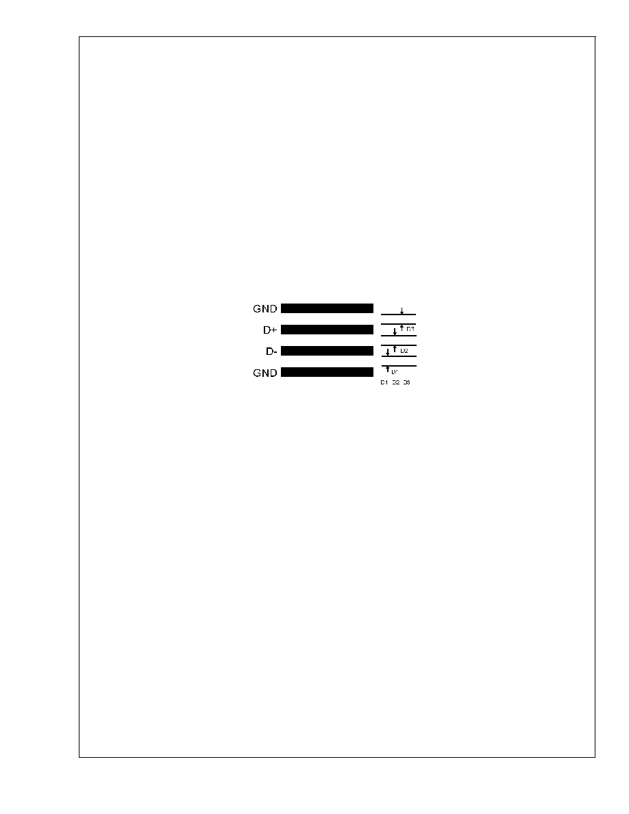
8.5 PCB Layout Recommendations for Minimizing
Noise
In a noisy environment, such as a processor mother board,
layout considerations are very critical. Noise induced on
traces running between the remote temperature diode sen-
sor and the LM87 can cause temperature conversion errors.
The following guidelines should be followed:
1.
Place a 0.1 µF power supply bypass capacitor as close
as possible to the V
CC
pin and the recommended 2.2 nF
capacitor as close as possible to the D+ and D- pins.
Make sure the traces to the 2.2 nF capacitor are
matched.
2.
Ideally, the LM87 should be placed within 10 cm of the
Processor diode pins with the traces being as straight,
short and identical as possible.
3.
Diode traces should be surrounded by a GND guard ring
to either side, above and below if possible. This GND
guard should not be between the D+ and D- lines. In the
event that noise does couple to the diode lines it would
be ideal if it is coupled common mode. That is equally to
the D+ and D- lines.
4.
Avoid routing diode traces in close proximity to power
supply switching or filtering inductors.
5.
Avoid running diode traces close to or parallel to high
speed digital and bus lines. Diode traces should be kept
at least 2 cm. apart from the high speed digital traces.
6.
If it is necessary to cross high speed digital traces, the
diode traces and the high speed digital traces should
cross at a 90 degree angle.
7.
The ideal place to connect the LM87's GND pin is as
close as possible to the Processors GND associated
with the sense diode. For the Pentium II this would be
pin A14.
Noise on the digital lines, overshoot greater than V
CC
and
undershoot less than GND, may prevent successful SMBus
communication with the LM87. SMBus no acknowledge is
the most common symptom, causing unnecessary traffic on
the bus. Although, the SMBus maximum frequency of com-
munication is rather low (400 kHz max) care still needs to be
taken to ensure proper termination within a system with mul-
tiple parts on the bus and long printed circuit board traces.
Additional noise immunity can be achieved by placing a re-
sistor (4.7k to 5.1k Ohms) in series with the SMBCLK input
as close to the LM87 as possible. This resistance, in con-
junction with the IC input capacitance, reduces high fre-
quency noise seen at the SMBCLK input and increases the
reliability of communications.
DS100995-35
FIGURE 9. Recommended Diode Trace Layout
LM87
www.national.com
18
Functional Description
(Continued)
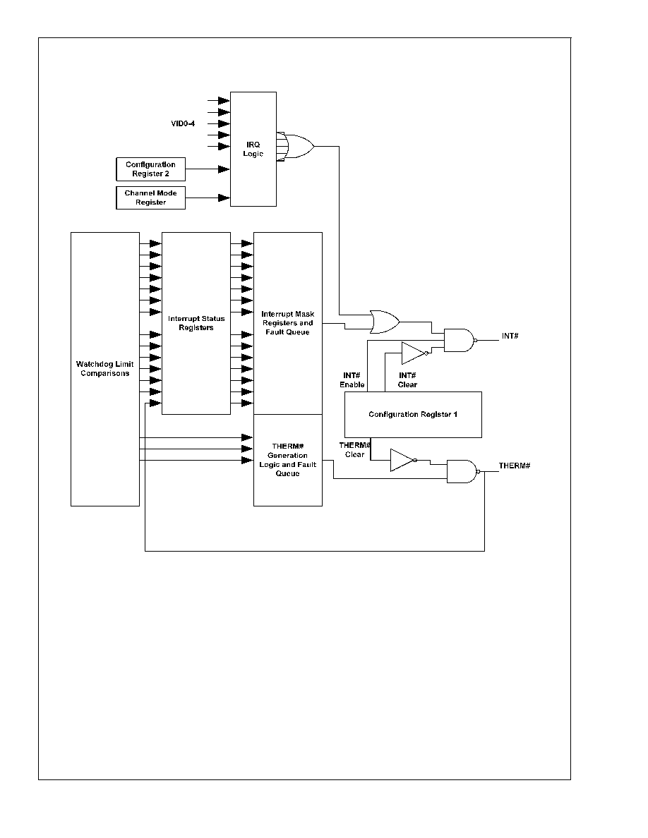
9.0 THE LM87 INTERRUPT STRUCTURE
Figure 10 depicts the Interrupt Structure of the LM87. The
LM87 can generate Interrupts as a result of each of its inter-
nal WATCHDOG registers on the analog, temperature, and
fan inputs.
External Interrupts can come from the following sources.
While the label suggests a specific type or source of Inter-
rupt, this label is not a restriction of its usage, and it could
come from any desired source:
∑
Chassis Intrusion:
This is an active high interrupt
from any type of device that detects and captures chassis
intrusion violations. This could be accomplished me-
chanically, optically, or electrically, and circuitry external
to the LM87 is expected to latch the event. The design of
the LM87 allows this input to go high even with no power
applied to the LM87, and no clamping or other interfer-
ence with the line will occur. This line can also be pulled
low for at least 20 ms by the LM87 to reset a typical
Chassis Intrusion circuit. This reset is activated by setting
Bit 7 of CI Clear Register (46h) high. The bit in the Reg-
ister is self-clearing.
∑
THERM# Input:
This is an active low interrupt that
would typically be generated by an external temperature
monitoring system. If the THERM# output is currently in-
active and this input is pulled low by an external circuit,
the THERM# Interrupt Status bit will be set. In addition,
the DAC output will be forced to full scale operation while
THERM# is pulled low by the external source. This allows
a separate thermal sensor to override the current fan
speed setting in an overtemperature situation not sensed
by the LM87. The DAC setting will return to normal when
the THERM# input is deactivated and the DAC setting
register is unaffected by the THERM# input condition.
DS100995-31
FIGURE 10. Interrupt Structure
LM87
www.national.com
19

Functional Description
(Continued)
∑
IRQ0-2:
These are active low inputs from any type of
external interrupt source. If enabled via the Channel
Mode Register (16h) the INT# output will be activated
whenever these inputs are pulled low. Since there are no
dedicated ISR bits that correspond to the IRQ inputs, the
VID status bits can be read to determine which IRQ input
is active. Similarly, to mask off these inputs as interrupt
sources, they must be disabled via the Channel Mode
Register (16h).
∑
IRQ3-4:
These are active high inputs from any type of
external interrupt source. If enabled via the Channel
Mode Register (16h) and Configuration Register 2 (4Ah),
the INT# output will be activated whenever these inputs
are driven high. Since there are no dedicated ISR bits
that correspond to the IRQ inputs, the VID status bits can
be read to determine which IRQ input is active. Similarly,
to mask off these inputs as interrupt sources, they must
be disabled via Configuration Register 2 (4Ah).
With the exception of the IRQ inputs and Hardware Tem-
perature errors, all interrupts are indicated in the two Inter-
rupt Status Registers. The INT# output has two mask regis-
ters, and individual masks for each Interrupt. As described in
Section 3.3, the hardware Interrupt line can also be enabled/
disabled in the Configuration Register.
The THERM# interrupt output is dedicated to temperature
and therefore is only related to internal and external tem-
perature readings, and the Low, High and Hardware tem-
perature limits.
9.1 INT# Interrupts
The INT# system combines several groups of error signals
together into a common output. These groups are; IRQ in-
puts, Voltage and Fan inputs, Temperature Values, and the
THERM# input. Each one of these groups or channels func-
tions a little differently.
The IRQ inputs provide the least complicated INT# opera-
tion. The IRQ input block is enabled by setting bit 7of the
Channel Mode Register (16h) to 0. Then the individual inputs
are enabled by setting the corresponding IRQ Enable bits to
1. If an IRQ input is enabled, and subsequently an input sig-
nal is asserted on that channel, the INT# output will be as-
serted. During the interrupt service routine, the INT# output
can be deasserted in a number of ways. The INT#_Clear bit
can be set during the ISR to prevent further interrupts from
occurring. Then the IRQ enable bit for the particular input
can be cleared to prevent that channel from causing further
interrupts. At this point the INT#_Clear bit can be cleared
and no further interrupts would be issued from this particular
IRQ input. Once the signal causing the IRQ has been re-
moved, the enable bit for that IRQ channel could be set
again.
Voltage, Fan, and Temperature High/Low errors are slightly
more complex in their generation of INT# outputs. All of
these error bits are stored in the Interrupt Status Registers at
43h, 44h and the Interrupt Status Mirror Registers at 4Ch
and 4Dh. These inputs are gated by the Interrupt Mask Reg-
isters and processed by the INT# state machine to generate
the INT# output.
Voltage and Fan error conditions are processed as follows.
Every time a round robin conversion cycle is completed, the
high/low limit comparisons for voltage and fan quantities are
updated. If a quantity is outside the limits, the appropriate In-
terrupt Status Register bit will be set. If the corresponding In-
terrupt Mask Register bit is 0, then the Status Bit will cause
the INT# output to be asserted. Reading the Interrupt Status
register will clear the Status Bit and cause the INT# output to
be deasserted. If the parameter is still outside the limits on
the next conversion, the status bit will again be set and it will
again cause an interrupt. If, on a subsequent conversion
cycle, the parameter returns within the High/Low limits be-
fore the Interrupt Status Registers are read, the Interrupt
Status bit will remain set and the INT# output will remain as-
serted.
Temperature High/Low errors are somewhat more compli-
cated. We will begin with the temperature value initially
within the High/Low limits and the corresponding Interrupt
Mask Bit = 0. If the temperature value rises above the high
limit, or below the low limit, the corresponding Interrupt Sta-
tus Register bit will be set. This will then cause an INT# to be
asserted. Reading the Interrupt Status Register will clear the
status bit and cause INT# to be deasserted. If the tempera-
ture value remains above the high limit during subsequent
conversion cycles, the Interrupt Status Bit will again be set,
but no new INT# will be generated from this source. INT#
may be reasserted if:
-- The temperature then transitions up or down through
the opposite limit to that originally exceeded.
-- The original limit crossed is programmed to a new
value and on a subsequent conversion cycle, the con-
verted temperature is outside the new limit. This would
cause the corresponding Interrupt Status Bit to be set,
causing a new INT# event.
-- An interrupt is generated by any other source, includ-
ing any other temperature error or the THERM# pin
being pulled low by an external signal.
The third group of signals that will generate INT# outputs are
Hardware Temperature errors, caused by temperatures ex-
ceeding the hardware limits stored at 13h, 14h, 17h, and
18h. Again, we will assume that the temperature initially is
below the Hardware Temperature setpoints. If the tempera-
ture on a subsequent conversion is above any of the values
stored in the Hardware Temperature Limit registers, the INT#
output will be asserted. Errors caused by exceeding these
limits cannot be cleared by reading the Interrupt Status Reg-
isters, and the INT# condition can only be cleared by clear-
ing the Thermal INT# Enable bit, by setting the INT#_Clear
bit or by disabling INT# by clearing the INT#_Enable bit. The
final INT# source to consider is the THERM# input/output.
THERM# can be pulled low by an external source to gener-
ate an INT# output. Pulling THERM# low with external cir-
cuitry sets the corresponding THERM# Interrupt Status Bit. If
this bit is not masked, it will cause INT# to be asserted.
Reading the Interrupt Status Registers will clear the status
bit and will cause INT# to be deasserted. If the external sig-
nal continues to pull THERM# low, the Interrupt Status Bit
will be reset at the completion of the next conversion cycle.
This will again assert the INT# output. Note that if the exter-
nal circuitry pulls THERM# low, but this pin is already low
due to the THERM# output being active, this external signal
cannot be sensed, and the THERM# Interrupt Status Bit will
not be set.
Interrupt Status Registers: Reading a Status Register will
output the contents of the Register, and reset the Register. A
subsequent read done before the analog "round-robin" moni-
toring loop is complete will indicate a cleared Register. Allow
at least 600 ms to allow all Registers to be updated between
reads. In summary, the Interrupt Status Register clears upon
being read, and requires at least 300 ms to be updated.
LM87
www.national.com
20

Functional Description
(Continued)
When the Interrupt Status Register clears, the hardware in-
terrupt line will also clear until the Registers are updated by
the monitoring loop.
Interrupt Status Mirror Registers: The Interrupt Status Mir-
ror Registers provide the same information that the Interrupt
Status Registers do. Reading the Status Mirror Registers,
however, does not reset the status bits.
Interrupt Mask Registers: All sources which are combined
to form the INT# output can be individually masked via the
two Interrupt Mask Registers at 43h, and 44h. The bits in the
mask registers correspond directly to the bits in the Interrupt
Status Registers. Setting an Interrupt Mask bit inhibits that
Interrupt Status Bit from generating an INT# interrupt. Clear-
ing a mask bit allows the corresponding status bit, if set, to
generate INT# outputs. Interrupt Status Bits will be set and
cleared regardless of the state of corresponding Interrupt
Mask Bits, the mask bits merely allow or prevent the status
bits from contributing to the generation of INT# outputs.
Enabling and Clearing INT#: The hardware Interrupt line
(INT#) is enabled by setting the INT#_Enable bit at Bit 1 of
Configuration Register 1. The INT# output can be cleared by
setting the INT#_Clear bit which is Bit 3 of Configuration
Register 1. When this bit is high, the LM87 monitoring loop
will stop. It will resume when the bit is low.
Thermal Interrupt Mask: In some applications, the user
may want to prevent all thermal error conditions from caus-
ing INT# interrupts. The Thermal INT# Mask bit (Bit 0 of Con-
figuration Register 2) is provided for this purpose. The
THERM# output discussed later is not affected by the status
of the Thermal INT# Mask bit and will function normally in re-
sponse to temperature error conditions. If the Thermal INT#
Mask bit is set, the interrupt status for internal and external
temperature, the THERM# input, and the hardware tempera-
ture error comparisons, will continue to be updated every
conversion cycle, but will not have any effect on the INT#
output.
9.2 SMBALERT#
The INT# I/O pin can alternatively be configured as an SM-
BALERT# output in conjunction with the SMBALERT# proto-
col. In this mode of operation, rather than connecting the
INT# /ALERT# pin to the system interrupt inputs, it will be
connected to the SMBALERT# input pin on the SMBus host.
When an INT#/ALERT# type error condition is detected, this
pin will notify the SMBus host that an SMBus device has an
SMBALERT# condition. The SMBus host will then access
the bus using the Alert Response Address (ARA) which is
0001100b. Only the device asserting the SMBALERT# sig-
nal will respond to the ARA, thus providing automatic identi-
fication of the device generating the SMBALERT#. After ac-
knowledging the slave address, the LM87 will disengage its
SMBALERT# output signal. For more information on the SM-
BALERT# protocol, please refer to the System Management
Bus specification. SMBALERT# is enabled by setting Bit 6 of
the Alert Response Enable register at 80h.
9.3 THERM# Interrupts
The THERM# I/O pin is dedicated to temperature related er-
ror conditions. It includes a built in pull-up resistor to mini-
mize external components. The THERM# Enable bit, Bit 2 of
Configuration Register 1 is used to enable the THERM# out-
put. The THERM# Clear bit, Bit 6 of Configuration Register 1,
when set to 1, clears the THERM# output. TheTHERM# out-
put operates in two different modes when processing ther-
mal error conditions, Default Mode and ACPI Mode, se-
lected by the state of the THERM# Interrupt Mode bit at Bit 3
of Configuration Register 2 (0 = Default, 1 = ACPI).
Default Mode:The THERM# ouput operates using a simple
comparison of temperature with the corresponding limit val-
ues. If any temperature value is outside a corresponding limit
in registers 37h, 39h, 2Bh, 38h, 3Ah, or 2Ch, the THERM#
output will go low. The output will remain asserted until it is
reset by: reading Interrupt Status Register 1, by setting the
THERM#CLR bit, or if the temperature falls below the low
limit for that sensor. When THERM# is cleared by reading
the status register, it may be set again after the next tem-
perature reading, if the temperature is still above the high
limit. When THERM# is cleared by setting THERM#CLR, it
cannot be re-asserted until this bit is cleared. If THERM# is
activated because a temperature value exceeds one of the
hardware limits in registers 13h, 14h, 17h, or 18h, or ex-
ceeds 126 degrees C, AOUT will be forced to the full scale
value. In this case, the THERM# output can only be cleared
by setting the THERM#CLR bit or if the temperature returns
to 5 degrees below the hardware limit. Regardless of how
THERM# is cleared, AOUT will be maintained at the full
scale value until the temperature returns to 5 degrees below
the hardware limit that was exceeded.
ACPI Mode: In ACPI mode, THERM# is only activated when
temperatures exceed the high limit settings in registers 13h,
14h, 17h, 18h or the safety limit of 126 degrees C. It will be
de-asserted if the temperature returns at least 5 degrees be-
low the limit. While THERM# is asserted, AOUT will be
driven to full scale to provide maximum cooling from a vari-
able speed fan.
THERM# also functions as an input. When an external active
low signal is applied to THERM#, it will set the THERM# in-
put Interrupt Status Bit and will cause AOUT to go to full
scale, regardless of the state of the THERM# Input Interrupt
Mask bit. If the Mask bit is cleared and INT# is enabled, an
INT# will be generated. The THERM# input function is not af-
fected by the THERM# operating mode.
9.4 Fault Queue
A Fault Queue is incorporated in the external temperature
monitoring sections of the LM87. This serves as a filter to
minimize false triggering caused by short duration or tran-
sient temperature events. The Fault Queue adds a counter
between the comparison logic and the Interrupt Status Reg-
ister and THERM# output circuitry. The Fault Queue has a
depth of 3, so three consecutive readings outside of limits is
required to set an external temperature Interrupt Status Bit
or generate a THERM# output. When the monitored tem-
perature is returning within limits, only one conversion within
limits is required to clear the status bit. In other words, the
fault queue is only active when travelling outside of the limits,
not when returning back within limits.
LM87
www.national.com
21
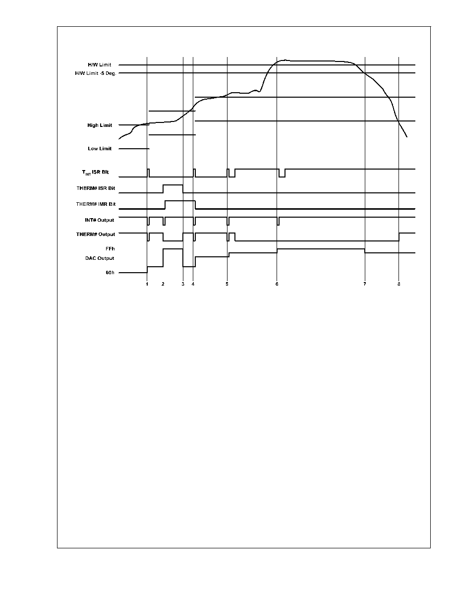
Functional Description
(Continued)
10.0 RESET# I/O
RESET# is intended to provide a master reset to devices
connected to this line. Setting Bit 4 in Configuration Register
1 high outputs a 20 ms low pulse on this line, at the end of
which Bit 4 in the Configuration Register automatically
clears. Again, the label for this pin is only its suggested use.
In applications where the RESET# capability is not needed it
can be used for any type of digital control that requires a 20
ms active low, open-drain output.
RESET# operates as an input when not activated by Con-
figuration Register 1. Setting this line low will reset all of the
registers in the LM87 to their power on default state. All
Value RAM locations will not be affected except for the DAC
Data Register.
11.0 NAND TREE TESTS
A NAND tree is provided in the LM87 for Automated Test
Equipment (ATE) board level connectivity testing. DACOut/
NTEST_IN, INT#, THERM#, V
+
and GND pins are excluded
from NAND tree testing. Taking DACOut/NTEST_IN high
during power up activates the NAND Tree test mode. After
the first SMBus access to the LM87 the NAND Tree test
mode is terminated and cannot be reactivated without re-
peating the power up sequence. To perform a NAND tree
test, all pins included in the NAND tree should be driven to 1
forcing the ADD/NTEST_OUT high. Each individual pin start-
ing with SMBData and concluding with RESET# (excluding
DACOut/NTEST_IN, INT#, THERM#, V
+
and GND) can be
taken low with the resulting toggle observed on the ADD/
NTEST_OUT pin. Allow for a typical propagation delay of
500 ns.
DS100995-32
FIGURE 11. LM87 Interrupt Structure
LM87
www.national.com
22
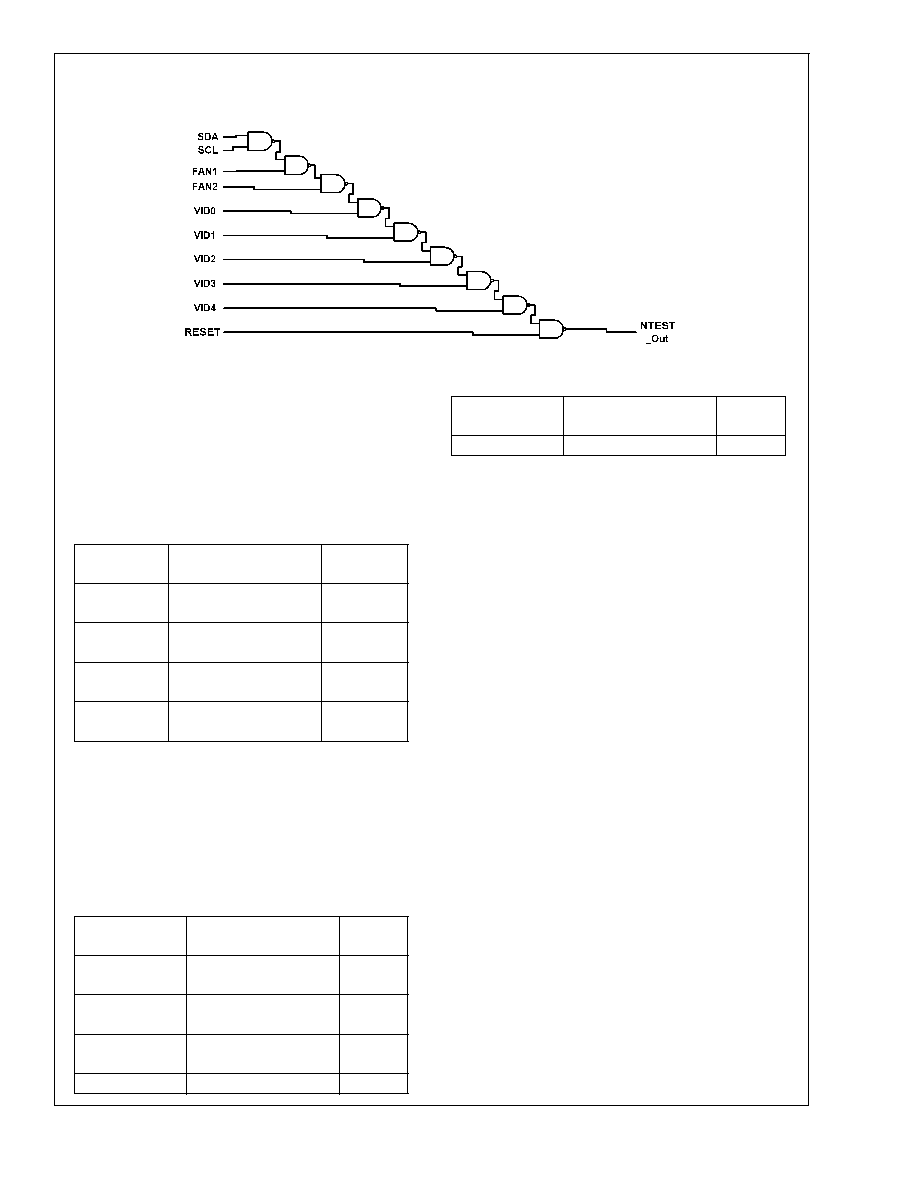
Functional Description
(Continued)
12.0 FAN MANUFACTURERS
Manufacturers of cooling fans with tachometer outputs are
listed below:
NMB Tech
9730 Independence Ave.
Chatsworth, California 91311
818 341-3355
818 341-8207
Model Num-
ber
Frame Size
Airflow
CFM
2408NL
2.36 in sq. X 0.79 in
9-16
(60 mm sq. X 20 mm)
2410ML
2.36 in sq. X 0.98 in
14-25
(60 mm sq. X 25 mm)
3108NL
3.15 in sq. X 0.79 in
25-42
(80 mm sq. X 20 mm)
3110KL
3.15 in sq. X 0.98 in
25-40
(80 mm sq. X 25 mm)
Mechatronics Inc.
P.O. Box 20
Mercer Island, WA 98040
800 453-4569
Various sizes available with tach output option.
Sanyo Denki America, Inc.
468 Amapola Ave.
Torrance, CA 90501
310 783-5400
Model Number
Frame Size
Airflow
CFM
109P06XXY601
2.36 in sq. X 0.79 in
11-15
(60 mm sq. X 20 mm)
109R06XXY401
2.36 in sq. X 0.98 in
13-28
(60 mm sq. X 25 mm)
109P08XXY601
3.15 in sq. X 0.79 in
23-30
(80 mm sq. X 20 mm)
109R08XXY401
3.15 in sq. X 0.98 in
21-42
Model Number
Frame Size
Airflow
CFM
(80 mm sq. X 25 mm)
DS100995-33
FIGURE 12. NAND Tree Test Structure
LM87
www.national.com
23
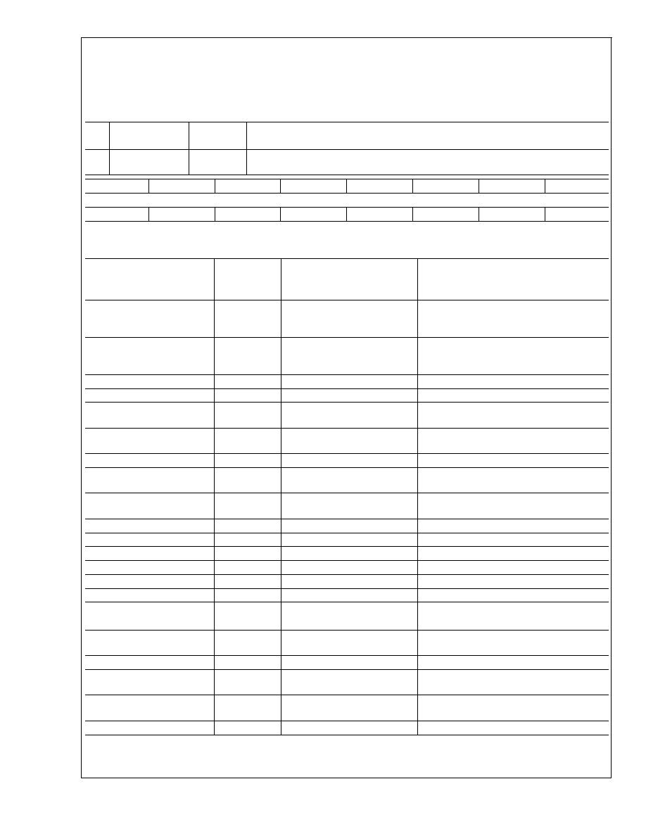
Functional Description
(Continued)
13.0 REGISTERS AND RAM
13.1 Address Register
The main register is the ADDRESS Register. The bit designations are as follows:
Bit
Name
Read/
Write
Description
7-0
Address
Pointer
Write
Address of RAM and Registers. See the tables below for detail.
Bit 7
Bit 6
Bit 5
Bit 4
Bit 3
Bit 2
Bit 1
Bit 0
Address Pointer (Power On default 00h)
A7
A6
A5
A4
A3
A2
A1
A0
13.2 Address Pointer Index (A7≠A0)
Registers and RAM
A6≠A0 in
Hex
Power On Value of
Registers:
Notes
<
7:0
>
in Binary
Internal Temp. Hardware
High Limit
13h
0100 0110
70 ∞C Default -
<
7:0
>
=0100 0110 - User
adjustable. Lockable by setting bit 1 of
register 4Ah.
External Temp. Hardware
High Limit
14h
0101 0101
85 ∞C Default -
<
7:0
>
=0101 0101 - User
adjustable. Lockable by setting bit 2 of
register 4Ah.
Test Register
15h
0000 0000
Always set to 00h
Channel Mode Register
16h
0000 0000
Internal Temp. Hardware
High Limit
17h
0100 0110
70 ∞C Default -
<
7:0
>
=0100 0110 - User
adjustable
External Temp. Hardware
High Limit
18h
0101 0101
85 ∞C Default -
<
7:0
>
=0101 0101 - User
adjustable
Value RAM
19h≠3Dh
Address 19h default=1111 1111
Company ID
3Eh
0000 0010
This designates the National
Semiconductor LM87.
Revision
3Fh
0000 0100
Revisions of this device will start with 1 and
increment by one.
Configuration Register 1
40h
0000 1000
Interrupt Status Register 1
41h
0000 0000
Interrupt Status Register 2
42h
0000 0000
Interrupt Mask Register 1
43h
0000 0000
Interrupt Mask Register 2
44h
0000 0000
CI Clear Register
46h
0000 0000
VID0-3/Fan Divisor
47h
<
7:4
>
= 0101;
Register
<
3:0
>
= VID3≠VID0
VID4 Register
49h
<
7:1
>
=1000 000;
<
0
>
=VID4
Configuration Register 2
4Ah
0000 0000
Interrupt Status Register 1
Mirror
4Ch
0000 0000
Interrupt Status Register 2
Mirror
4Dh
0000 0000
SMBALERT# Enable
80h
0010 0000
LM87
www.national.com
24
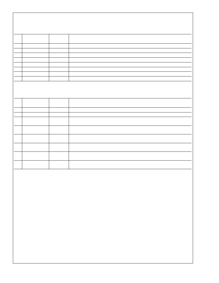
Functional Description
(Continued)
13.3 Test Register -- Address 15h
Power on default ≠
<
7:0
>
= 00001000 binary
Bit
Name
Read/
Write
Description
0
Shutdown
Read/Write
A one places the LM87 in a lower power
Shutdown
mode.
1
Reserved
Read/Write
2
Reserved
Read/Write
3
Reserved
Read/Write
4
Reserved
Read/Write
5
Reserved
Read/Write
6
Reserved
Read/Write
7
Reserved
Read/Write
13.4 Channel Mode Register -- Address 16h
Power on default ≠
<
7:0
>
= 00001000 binary
Bit
Name
Read/
Write
Description
0
FAN1/AIN1
Read/Write
A one enables the input as AIN1, a zero enables the input as FAN1.
1
FAN2/AIN2
Read/Write
A one enables the input as AIN2, a zero enables the input as FAN2.
2
2.5V,
V
CCP2
/D2
Read/Write
A one enables the 2.5V, V
CCP2
/D2 inputs as a second remote diode temperature
input.
3
Int. V
CC
Range
Read/Write
A one configures the LM87 for 5.0V V
CC
measurement. A zero configures it for 3.3V
V
CC
measurement.
4
IRQ0 EN
Read/Write
A one enables pin 24 as an active high interrupt input. Bit 7 must also be set to
configure the VID/IRQ inputs to IRQ mode.
5
IRQ1 EN
Read/Write
A one enables pin 23 as an active high interrupt input. Bit 7 must also be set to
configure the VID/IRQ inputs to IRQ mode.
6
IRQ2 EN
Read/Write
A one enables pin 22 as an active high interrupt input. Bit 7 must also be set to
configure the VID/IRQ inputs to IRQ mode.
7
VID/IRQ
Read/Write
A one configures the VID/IRQ inputs as Interrupt Inputs. A zero configures the
VID/IRQ inputs as VID inputs only.
LM87
www.national.com
25
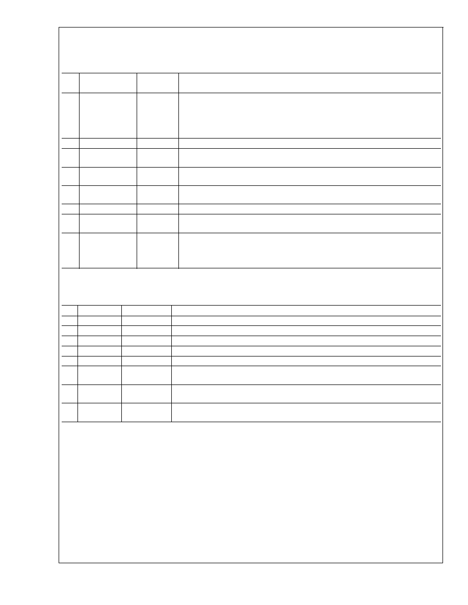
Functional Description
(Continued)
13.5 Configuration Register -- Address 40h
Power on default ≠
<
7:0
>
= 00001000 binary
Bit
Name
Read/
Write
Description
0
Start
Read/Write
A one enables startup of monitoring operations, a zero puts the part in standby mode.
Note: The outputs of Interrupt pins will not be cleared if the user writes a zero to this
location after an interrupt has occurred, unlike the "INT_Clear" bit.
At start up, limit checking functions and scanning begin. Note, all limits should be set
in the Value RAM before setting this bit HIGH.
1
INT# Enable
Read/Write
A one enables the INT# Interrupt output.
2
THERM#
Enable
Read/Write
A one enables the THERM# Interrupt output.
3
INT#_Clear
Read/Write
A one disables the INT# output without affecting the contents of Interrupt Status
Registers. The device will stop monitoring. It will resume upon clearing of this bit.
4
RESET#
Read/Write
A one outputs a 20 ms minimum active low reset signal at RESET#. This bit is cleared
once the pulse has gone inactive.
5
Reserved
Read/Write
6
THERM#_Clear
Read/Write
A one disables the THERM# output without affecting the contents of Interrupt Status
Registers.
7
INITIALIZATION
Read/Write
A one restores power on default values to the Configuration Register, Interrupt Status
Registers, Interrupt Mask Registers, CI Clear Register, VID/Fan Divisor Register,
VID4, Temperature Configuration Register, and the Extended Mode Registers. This bit
clears itself since the power on default is zero.
13.6 Interrupt Status Register 1 -- Address 41h
Power on default ≠
<
7:0
>
= 0000 0000 binary
Bit
Name
Read/Write
Description
0
+2.5Vin
Read Only
A one indicates a High or Low limit has been exceeded.
1
Vccp1
Read Only
A one indicates a High or Low limit has been exceeded.
2
Vcc
Read Only
A one indicates a High or Low limit has been exceeded.
3
+5Vin
Read Only
A one indicates a High or Low limit has been exceeded.
4
Int. Temp.
Read Only
A one indicates a High or Low limit has been exceeded.
5
Ext.
Temp.
Read Only
A one indicates a High or Low limit has been exceeded.
6
FAN1/AIN1
Read Only
A one indicates the fan count limit has been exceeded or an AIN1 High or Low limit has
been exceeded.
7
FAN2/AIN2
Read Only
A one indicates the fan count limit has been exceeded or an AIN2 High or Low limit has
been exceeded.
LM87
www.national.com
26
Functional Description
(Continued)
13.7 Interrupt Status Register 2 -- Address 42h
Power on default ≠
<
7:0
>
= 0000 0000 binary
Bit
Name
Read/Write
Description
0
+12Vin
Read Only
A one indicates a High or Low limit has been exceeded.
1
Vccp2
Read Only
A one indicates a High or Low limit has been exceeded.
2
Reserved
Read Only
3
Reserved
Read Only
4
CI
Read Only
A one indicates the CI (Chassis Intrusion) input has gone high.
5
THERM#
Read Only
A one indicates the THERM# input has been pulled low by external circuitry.
6
D1 Fault
Read Only
A one indicates the D1 inputs are shorted to Vcc or open circuit.
7
D2 Fault
Read Only
A one indicates the D2 inputs are shorted to Vcc or open circuit.
13.8 Interrupt Mask Register 1 -- Address 43h
Power on default ≠
<
7:0
>
= 0000 0000 binary
Bit
Name
Read/
Write
Description
0
+2.5Vin/D2+
Read/Write
A one disables the corresponding interrupt status bit for INT# interrupt.
1
Vccp1
Read/Write
A one disables the corresponding interrupt status bit for INT# interrupt.
2
Vcc
Read/Write
A one disables the corresponding interrupt status bit for INT# interrupt.
3
+5Vin
Read/Write
A one disables the corresponding interrupt status bit for INT# interrupt.
4
Int. Temp.
Read/Write
A one disables the corresponding interrupt status bit for INT# interrupt.
5
Ext.
Temp.
Read/Write
A one disables the corresponding interrupt status bit for INT# interrupt.
6
FAN1/AIN1
Read/Write
A one disables the corresponding interrupt status bit for INT# interrupt.
7
FAN2/AIN2
Read/Write
A one disables the corresponding interrupt status bit for INT# interrupt.
13.9 Interrupt Mask Register 2 -- Address 44h
Power on default ≠
<
7:0
>
= 0000 0000 binary
Bit
Name
Read/
Write
Description
0
+12Vin
Read/Write
A one disables the corresponding interrupt status bit for INT# interrupt.
1
Vccp2
Read/Write
A one disables the corresponding interrupt status bit for INT# interrupt.
2
Reserved
Read/Write
3
Reserved
Read/Write
4
Chassis Intrusion
Read/Write
A one disables the corresponding interrupt status bit for INT# interrupt.
5
THERM#
Read/Write
A one disables the corresponding interrupt status bit for INT# interrupt.
6
D1 Fault
Read/Write
A one disables the corresponding interrupt status bit for INT# interrupt.
7
D2 Fault
Read/Write
A one disables the corresponding interrupt status bit for INT# interrupt.
13.10 Reserved Register -- Address 45h
Power on default ≠
<
7:0
>
= 00h. Read/Write for backwards compatibility.
13.11 CI Clear Register -- Address 46h
Power on default ≠
<
7:0
>
= 0000 0000 binary
Bit
Name
Read/
Write
Description
0-6
Reserved
Read/Write
7
CI Clear
Read/Write
A one outputs a minimum 20 ms active low pulse on the Chassis Intrusion pin. The
register bit self clears after the pulse has been output.
LM87
www.national.com
27
Functional Description
(Continued)
13.12 VID0-3/Fan Divisor Register -- Address 47h
Power on default ≠
<
7:4
>
is 0101, and
<
3:0
>
is mapped to VID
<
3:0
>
Bit
Name
Read/Write
Description
0-3
VID
<
3:0
>
Read Only
The VID
<
3:0
>
inputs from the Pentium/PRO power supplies that indicate the
operating voltage (e.g. 1.5 V to 2.9 V).
4-5
FAN1 RPM
Control
Read/Write
FAN1 Speed Control.
<
5:4
>
= 00 - divide by 1;
<
5:4
>
= 01 - divide by 2;
<
5:4
>
= 10 - divide by 4;
<
5:4
>
= 11 - divide by 8.
6-7
FAN2 RPM
Control
Read/Write
FAN2 Speed Control.
<
7:6
>
= 00 - divide by 1;
<
7:6
>
= 01 - divide by 2;
<
7:6
>
= 10 - divide by 4;
<
7:6
>
= 11 - divide by 8.
13.13 VID4 Register -- Address 49h
Power on default ≠
<
7:1
>
= 100 000,
<
0
>
= VID4.
Bit
Name
Read/Write
Description
0
VID4
Read Only
Bit 4 of VID data from the CPU or power supply that indicates the operating
voltage (e.g. 1.5 V to 2.9 V).
1-7
Reserved
Read/Write
13.14 Configuration Register 2 -- Address 4Ah
Power on default ≠
<
7:0
>
= 0000 0000 binary
Bit
Name
Read/Write
Description
0
Thermal INT#
Mask
Read/Write
When this bit is set to 1, thermal error events will not affect the INT# interrupt
output. THERM# outputs will still function normally.
1
Local Temp.
Register Write
Once Bit
Read/Write
Once
When set to 1, this bit locks in the value set in the Internal Temp. high limit
register at 0x13h. The value cannot be changed until a power on reset is
performed.
2
Remote Temp.
Register Write
Once Bit
Read/Write
Once
When set to 1, this bit locks in the value set in the External Temp. high limit
register at 0x14h. The value cannot be changed until a power on reset is
performed.
3
THERM# Interrupt
Mode
Read/Write
When set to 0, the THERM# output functions in Default mode. When set to 1, the
THERM# output functions in ACPI mode.
4-5
Reserved
6
IRQ3 Enable
Read/Write
When set to 1, VID3/IRQ3 is enabled as an active high interrupt input (if the
IRQEN bit is set in bit 7 of the Channel Mode Register).
7
IRQ4 Enable
Read/Write
When set to 1, VID4/IRQ4 is enabled as an active high interrupt input (if the
IRQEN bit is set in bit 7 of the Channel Mode Register).
LM87
www.national.com
28
Functional Description
(Continued)
13.15 Interrupt Status Register 1 Mirror -- Address 4Ch
Power on default ≠
<
7:0
>
= 0000 0000 binary
Bit
Name
Read Only
Description
0
+2.5Vin
Read Only
A one indicates a High or Low limit has been exceeded.
1
Vccp1
Read Only
A one indicates a High or Low limit has been exceeded.
2
Vcc
Read Only
A one indicates a High or Low limit has been exceeded.
3
+5Vin
Read Only
A one indicates a High or Low limit has been exceeded.
4
Int. Temp.
Read Only
A one indicates a High or Low limit has been exceeded.
5
Ext.
Temp.
Read Only
A one indicates a High or Low limit has been exceeded.
6
FAN1/AIN1
Read Only
A one indicates the fan count limit has been exceeded or an AIN1 High or Low limit has
been exceeded.
7
FAN2/AIN2
Read Only
A one indicates the fan count limit has been exceeded or an AIN2 High or Low limit has
been exceeded.
13.16 Interrupt Status Register 2 Mirror -- Address 4Dh
Power on default ≠
<
7:0
>
= 0000 0000 binary
Bit
Name
Read Only
Description
0
+12Vin
Read Only
A one indicates a High or Low limit has been exceeded.
1
Vccp2
Read Only
A one indicates a High or Low limit has been exceeded.
2
Reserved
Read Only
3
Reserved
Read Only
4
CI
Read Only
A one indicates the CI (Chassis Intrusion) input has gone high.
5
THERM#
Read Only
A one indicates the THERM# input has been pulled low by external circuitry.
6
D1 Fault
Read Only
A one indicates the D1 inputs are shorted to Vcc or open circuit.
7
D2 Fault
Read Only
A one indicates the D2 inputs are shorted to Vcc or open circuit.
13.17 SMBALERT# Enable -- Address 80h
Power on default ≠
<
7:0
>
= 0000 0000 binary
Bit
Name
Read/Write
Description
0
Reserved
Read Only
1
Reserved
Read Only
2
Reserved
Read Only
3
Reserved
Read Only
4
Reserved
Read Only
5
Reserved
Read Only
6
SMBALERT#
Enable
Read/Write
A one enables the SMBALERT# mode of operation.
7
Reserved
Read Only
LM87
www.national.com
29

Functional Description
(Continued)
13.18 Value RAM -- Address 15h≠3Fh
Address A6≠A0
Description
19h
DAC data register; power on default
<
7:0
>
=1111 1111 binary
20h
+2.5V/External Temperature 2 reading
21h
Vccp1 reading
22h
+Vcc reading
23h
+5V reading
24h
+12V reading
25h
Vccp2 reading
26h
External Temperature 1 reading
27h
Internal Temperature reading
28h
FAN1/AIN1 reading
Note: For the FAN reading, this location stores the number of counts of the internal clock per
revolution.
29h
FAN2/AIN2 reading
Note: For the FAN reading, this location stores the number of counts of the internal clock per
revolution.
2Ah
Reserved
2Bh
+2.5V High Limit/External Temperature 2 High Limit
2Ch
+2.5V Low Limit/External Temperature 2 Low Limit
2Dh
Vccp1 High Limit
2Eh
Vccp1 Low Limit
2Fh
+3.3V High Limit
30h
+3.3V Low Limit
31h
+5V High Limit
32h
+5V Low Limit
33h
+12V High Limit
34h
+12V Low Limit
35h
Vccp2 High Limit
36h
Vccp2 Low Limit
37h
External Temperature 1 High Limit
38h
External Temperature 1 Low Limit
39h
Internal Temperature High Limit
3Ah
Internal Temperature Low Limit
3Bh
FAN1Count Limit/AIN1 High Limit
Note: It is the number of counts of the internal clock for the Low Limit of the fan speed.
3Ch
FAN2 Fan Count Limit/AIN2 High Limit
Note: It is the number of counts of the internal clock for the Low Limit of the fan speed.
3Dh
Reserved
3Eh
Company Identification. The number in this register identifies National Semiconductor LM87 (0000
0010)
3Fh
Stepping Register LM87 revision number (0000 0100)
Note: Setting all ones to the high limits for voltages and fans (0111 1111 binary for temperature) means interrupts will never be generated except the case when volt-
ages go below the low limits.
For voltage input high limits, the device is doing a greater than comparison. For low limits, however, it is doing a less than or equal to comparison.
LM87
www.national.com
30
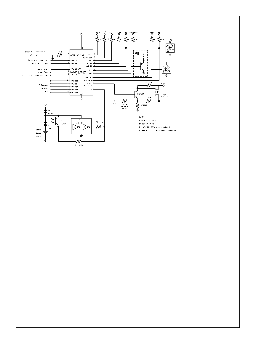
Typical Application
DS100995-23
FIGURE 13. In this PC application the LM87 monitors temperature, fan speed for 2 fans, and 6 power
supply voltages. It also monitors an optical chassis intrusion detector.
The LM87 provides a DAC output that can be used to control fan speed.
LM87
www.national.com
31
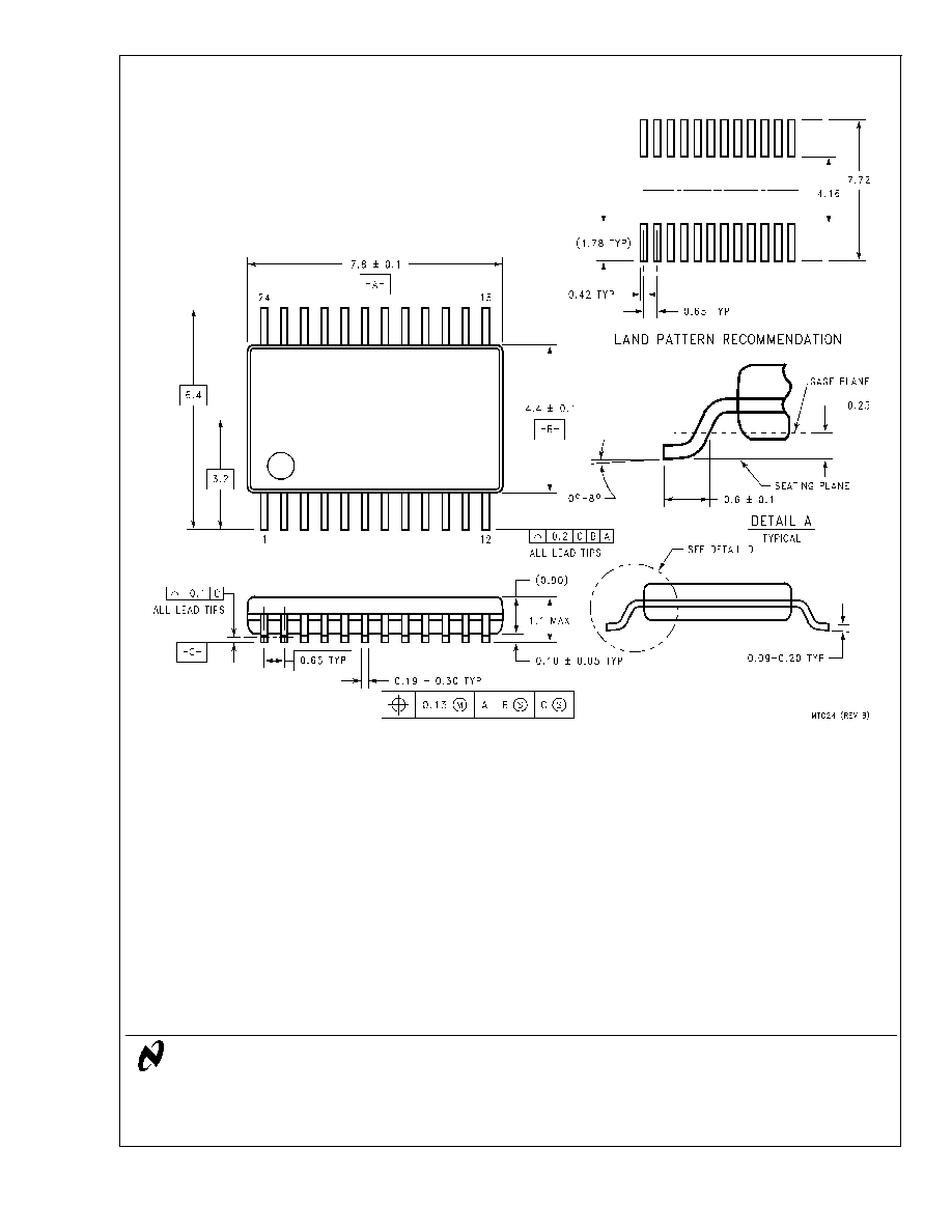
Physical Dimensions
inches (millimeters) unless otherwise noted
LIFE SUPPORT POLICY
NATIONAL'S PRODUCTS ARE NOT AUTHORIZED FOR USE AS CRITICAL COMPONENTS IN LIFE SUPPORT
DEVICES OR SYSTEMS WITHOUT THE EXPRESS WRITTEN APPROVAL OF THE PRESIDENT AND GENERAL
COUNSEL OF NATIONAL SEMICONDUCTOR CORPORATION. As used herein:
1. Life support devices or systems are devices or
systems which, (a) are intended for surgical implant
into the body, or (b) support or sustain life, and
whose failure to perform when properly used in
accordance with instructions for use provided in the
labeling, can be reasonably expected to result in a
significant injury to the user.
2. A critical component is any component of a life
support device or system whose failure to perform
can be reasonably expected to cause the failure of
the life support device or system, or to affect its
safety or effectiveness.
National Semiconductor
Corporation
Americas
Tel: 1-800-272-9959
Fax: 1-800-737-7018
Email: support@nsc.com
National Semiconductor
Europe
Fax: +49 (0) 180-530 85 86
Email: europe.support@nsc.com
Deutsch Tel: +49 (0) 69 9508 6208
English
Tel: +44 (0) 870 24 0 2171
FranÁais Tel: +33 (0) 1 41 91 8790
National Semiconductor
Asia Pacific Customer
Response Group
Tel: 65-2544466
Fax: 65-2504466
Email: ap.support@nsc.com
National Semiconductor
Japan Ltd.
Tel: 81-3-5639-7560
Fax: 81-3-5639-7507
www.national.com
24-Lead TSSOP
Order Number LM87CIMT
NS Package Number MTC24B
LM87
Serial
Interface
System
Hardware
Monitor
with
Remote
Diode
T
emperature
Sensing
National does not assume any responsibility for use of any circuitry described, no circuit patent licenses are implied and National reserves the right at any time without notice to change said circuitry and specifications.