LM88
Factory Programmable Dual Remote-Diode Thermostat
General Description
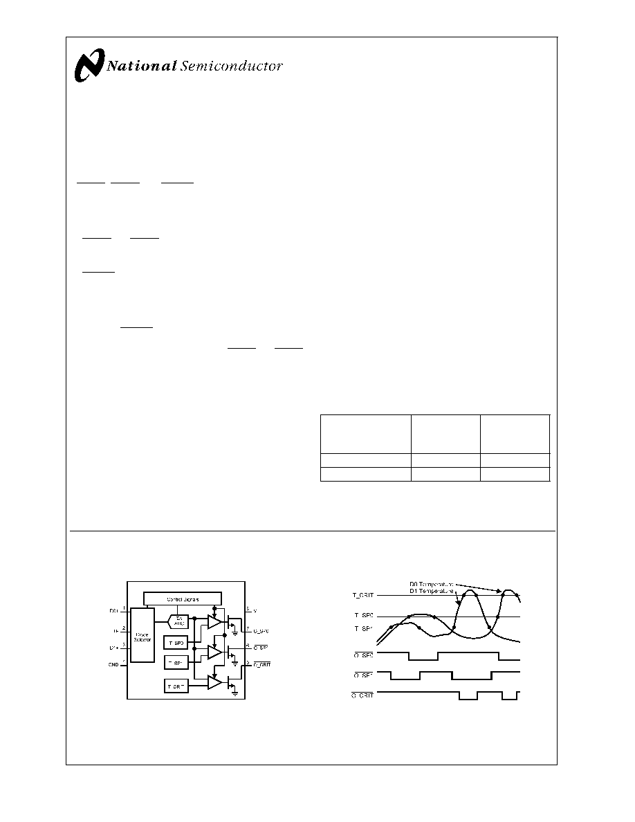
The LM88 is a dual remote-diode temperature sensor with 3
digital comparators. The LM88 has 3 open-drain outputs
(O_SP0, O_SP1 and O_CRIT) that can be used as inter-
rupts or to signal system shutdown. The digital comparators
can be factory programmed to make a greater than or less
than comparison. When programmed for a greater than
comparison outputs:
O_SP0 and O_SP1 activate when the temperatures mea-
sured by D0 or D1 exceed the associated setpoints of
T_SP0 or T_SP1.
O_CRIT activates when the temperature measured by
either D0 or D1 exceeds setpoint T_CRIT.
T_CRIT can be set at 1∞C intervals from -40∞C to +125∞C.
T_SP0 and T_SP1 can be set at 4∞C intervals in the range of
T_CRIT +127∞C/-128∞C. Hysteresis for all comparators is
set to 1∞C. O_CRIT, in conjunction with T_CRIT, could be
used to prevent catastrophic damage to key subsystems
such as notebook Card Bus cards while O_SP0 and O_SP1,
in conjunction with T_SP0 and T_SP1, can warn of an
impending failure.
The LM88 is available in an 8-lead mini-small-outline pack-
age.
Applications
n
Microprocessor Thermal Management
n
Appliances
n
Portable Battery Powered Systems
n
Fan Control
n
Industrial Process Control
n
HVAC Systems
n
Remote Temperature Sensing
n
Electronic System Protection
Features
n
2 external remote diode input channels
n
3 digital comparator outputs, 1 per remote diode and
one T_CRIT common to both
n
Factory programmable greater than or less than
comparisons
n
1∞C comparator hysteresis
n
2 setpoints, T_SP0 and T_SP1, factory programmable in
4∞C intervals
n
1 setpoint, T_CRIT, factory programmable in 1∞C
intervals
n
Active Low open-drain digital outputs
n
8-pin mini-SO plastic package
Key Specifications
j
Power Supply Voltage
2.8V≠3.8V
j
Power Supply Current
1.5 mA (max)
j
LM88 Temperature Range
-40∞C to +85∞C
j
Diode Setpoint Temperature
Range
0∞C to +125∞C
j
Temperature Trip Point Accuracy:
Diode Junction
Temperature
(T
DJ
)
LM88CIM
Accuracy
LM88CIM
Temperature
Range
+45∞C to +85∞C
±
3∞C (max)
-40∞C to +85∞C
+60∞C to +100∞C
±
3∞C (max)
-40∞C to +85∞C
Note: These are sample ranges. Contact factory for other
ranges.
Simplified Block Diagram and Connection Diagram
MSOP-8/MUA08A Package
10132601
Top View
10132602
For simplicity, the effects of the hysteresis are not shown in the
temperature response diagram.
August 2001
LM88
Factory
Programmable
Dual
Remote-Diode
Thermostat
© 2001 National Semiconductor Corporation
DS101326
www.national.com

Simplified Block Diagram and Connection Diagram
(Continued)
Order Number
Device
Marking
NS Package
Number
Transport
Media
T_SP0
(∞C)
T_SP1
(∞C)
T_CRIT
(∞C)
S etpoint
Accuracy
(∞C)
LM88CIMM-A
T08A
MUA08A
or
MSOP-8
Rail
61
49
80
±
3
LM88CIMMX-A
Tape and
Real
LM88CIMM-B
T08A
MUA08A
or
MSOP-8
Rail
41
49
60
±
3
LM88CIMMX-B
Tape and
Real
For other setpoints please contact the factory. Performance is dependent on temperature range.
Typical Application
10132613
FIGURE 1. Thermal Protection for Pentium
Æ
Processor and Graphics Chip
LM88
www.national.com
2
Absolute Maximum Ratings
(Note 1)
Input Voltage
6V
Input Current at any pin (Note 2)
5mA
Package Input Current (Note 2)
20mA
Package Dissipation at T
A
= 25∞C
(Note 4)
900mW
Soldering Information
MSOP Package (Note 6) :
Vapor Phase (60 seconds)
215∞C
Infrared (15 seconds)
220∞C
Storage Temperature
-65∞C to + 150∞C
ESD Susceptibility (Note 5)
Human Body Model
Machine Model
2500V
250V
Operating Ratings
(Note 1)
Operating Temperature
Range
T
MIN
T
T
MAX
LM88CIMM
-40∞C
T
A
+85∞C
Remote Diode Junction
0∞C
T
DJ
+125∞C
Positive Supply Voltage (V
+
)
+2.8V to +3.8V
Maximum V
O_CRIT
, V
O_SP0
and V
O_SP1
+5.5V
LM88 Electrical Characteristics
The following specifications apply for 2.8V
DC
V
+
3.8V
DC
unless otherwise specified. Boldface limits apply for T
A
= T
J
=
T
MIN
to T
MAX
; all other limits T
A
= T
J
= 25∞C unless otherwise specified.
Typical
LM88CIMM
Units
Symbol
Parameter
Conditions
(Note 7)
Limits
(Limits)
(Note 8)
Temperature Sensor
Setpoint Temperature Accuracy (Note 9)
+60∞C
T
DJ
+100∞C
±
3
∞C (max)
+45∞C
T
DJ
+85∞C
+30∞C
T
DJ
+70∞C
Setpoint Hysteresis
1
∞C (min)
1
∞C (max)
Output Update Rate
920
ms (max)
V
D-
, V
D0
and V
D1
Analog Inputs
I
D+SOURCE
Diode Source Current
(D+ - D-)=0.65; high
level
120
210
µA (max)
46
µA (min)
(D+ - D-)=0.65; low
level
12
21
µA (max)
4.6
µA (min)
V
D-Out
D- Output Source Voltage
0.7
V
LM88 Electrical Characteristics
The following specifications apply for 2.8V
DC
V
+
3.8V
DC
unless otherwise specified. Boldface limits apply for T
A
= T
J
=
T
MIN
to T
MAX
; all other limits T
A
= T
J
= 25∞C unless otherwise specified.
Symbol
Parameter
Conditions
Typical
Limits
Units
(Note 7)
(Note 8)
(Limits)
V
+
Power Supply
I
S
Supply Current
1.5
mA (max)
Digital Outputs
I
OUT("1")
Logical "1" Output Leakage
Current (Note 10)
V
OUT
=V
+
- 0.6V
where V
+
=3.8V to
2.8V
2
µA (max)
V
OUT
=V
+
=3.8V to
2.8V
40
µA (max)
V
OUT("0")
Logical "0" Output Voltage
I
OUT
= +3 mA
0.4
V (max)
Note 1: Absolute Maximum Ratings indicate limits beyond which damage to the device may occur. Operating Ratings indicate conditions for which the device is
functional, but do not guarantee specific performance limits. For guaranteed specifications and test conditions, see the Electrical Characteristics. The guaranteed
specifications apply only for the test conditions listed. Some performance characteristics may degrade when the device is not operated under the listed test
conditions.
LM88
www.national.com
3
LM88 Electrical Characteristics
(Continued)
Note 2: When the input voltage (V
I
) at any pin exceeds the power supply (V
I
<
GND or V
I
>
V
+
), the current at that pin should be limited to 5mA. The 20mA
maximum package input current rating limits the number of pins that can safely exceed the power supplies with an input current of 5mA to four.
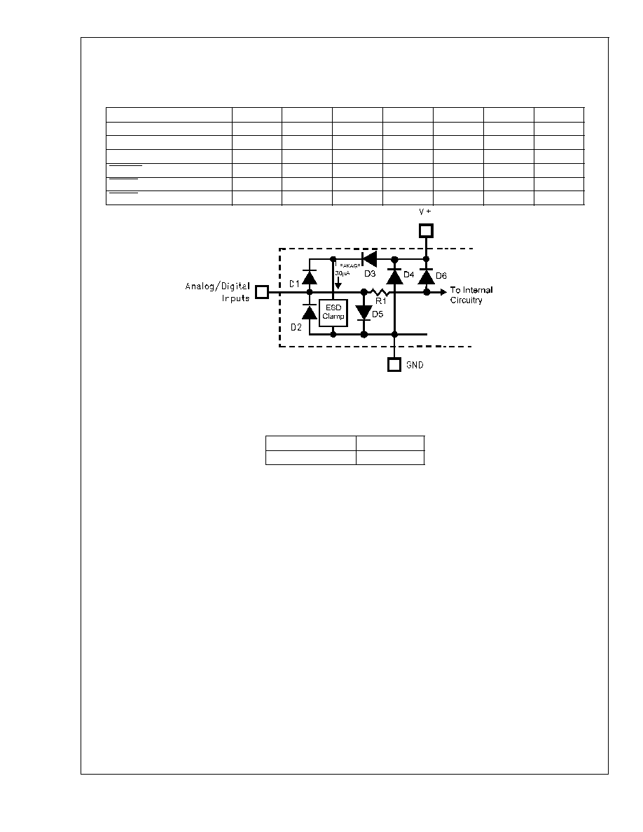
Note 3: Parasitics or ESD protection circuitry are shown in the diagram found below. The ESD Clamp circtuitry is triggered on when there is an ESD event. The table
maps what devices appear on the different pins.
Pin Name
D1
D2
D3
D4
D5
D6
R1
D0+
X
X
X
X
X
50
D-
X
X
X
X
X
X
50
D1+
X
X
X
X
X
50
O_CRIT
X
X
X
X
0
O_SP1
X
X
X
X
0
O_SP0
X
X
X
X
0
10132604
Note 4: The maximum power dissipation must be derated at elevated temperatures and is dictated by T
Jmax
(maximum junction temperature),
JA
(junction to
ambient thermal resistance) and T
A
(ambient temperature). The maximum allowable power dissipation at any temperature is P
D
= (T
Jmax
≠T
A
)/
JA
or the number
given in the Absolute Maximum Ratings, whichever is lower. For this device, T
Jmax
= 125∞C. For this device the typical thermal resistance (
JA
) of the different
package types when board mounted follow:
Package Type
JA
MUA08A
250∞C/W
Note 5: The human body model is a 100pF capacitor discharged through a 1.5k
resistor into each pin. The machine model is a 200pF capacitor discharged directly
into each pin.
Note 6: See the URL "http://www.national.com/packaging/" for other recomdations and methods of soldering surface mount devices.
Note 7: Typicals are at T
J
= T
A
= 25∞C and represent most likely parametric norm.
Note 8: Limits are guaranteed to National's AOQL (Average Outgoing Quality Level).
Note 9: These are sample temperature ranges, contact the factory for other temperature ranges. Performance is dependent on temperature range.
Note 10: The two I
OH
specifications are intended to describe two operating regions of the output voltage. In Region 1, V
+
- 0.6V and below, there is normal leakage
current, 2µA (max). In Region 2, V
+
- 0.6V to V
+
, there is additional current flowing caused by the ESD protection circuitry (see Figure in Note 3). The maximum
current flow is under short circuit conditions as specified at 40µA (max). Under normal operating conditions a pull-resistor (R) will be used. The voltage drop across
this pull-up resistor caused by the 2µA normal leakage current with large values of R (much greater than 100k) will bias diode D1 into the cutoff region causing the
additional current to be negligible in the voltage drop calculation. With low values of R more current will flow as in the case of a 1.1k pull-up, 20µA may flow causing
less than 22mV of voltage drop.
LM88
www.national.com
4
1.0 Functional Description
1.1 PIN DESCRIPTIONS
V
+
This is the positive supply voltage pin, which has
a range of 2.8 to 3.8 volts. This pin should be
bypassed with a 0.1µF capacitor to ground.
GND
This is the ground pin.
D0+, D1+ These pins connect to the positive terminal of the
diodes (e.g. a 2N3904 collector base shorted or a
Pentium thermal diode anode) and provide the
source current for forward biasing the diodes for
the temperature measurement. During a tem-
perature conversion, the current source switches
between 120µA and 12µA. The diodes are
sampled sequentially.
D-
This pin should be connected to the negative pin
of each diode (e.g. a 2N3904 emitter or a Pen-
tium thermal diode cathode). A star connection is
recommended. Separate traces should be routed
from this pin to each diode cathode. This pin
biases the negative diode terminals to approxi-
mately 0.7V.
O_CRIT
This is an active-low open-drain digital output. It
goes LOW when a comparison of either diode
temperature reading to the setpoint T_CRIT is
true. It returns to HIGH when the comparison of
the diode temperature, that caused the true con-
dition, to T_CRIT
±
1∞C is false. The CRIT com-
parator can be factory programmed to make a
greater than or less than comparison. (See Sec-
tion 1.3 LM88 OPTIONS)
O_SP1
This is an active-low open-drain digital output. It
goes LOW when the comparison of the tempera-
ture reading of diode one to the value of T_SP1 is
true. The SP1 comparator has a built in hyster-
esis of 1∞C. Therefore, O_SP1 returns to HIGH
when diode one's temperature comparison to the
value of T_SP1
±
1∞C is false. The SP1 compara-
tor can be factory programmed to make a greater
than or less than comparison.(See Section 1.3
LM88 OPTIONS)
O_SP0
This is an active-low open-drain digital output. It
goes LOW when the comparison of the tempera-
ture reading of diode one to the value of T_SP0 is
true. The SP0 comparator has a built in hyster-
esis of 1∞C. Therefore, O_SP0 returns to HIGH
when diode one's temperature comparison to the
value of T_SP0
±
1∞C is false. The SP0 compara-
tor can be factory programmed to make a greater
than or less than comparison.(See Section 1.3
LM88 OPTIONS)
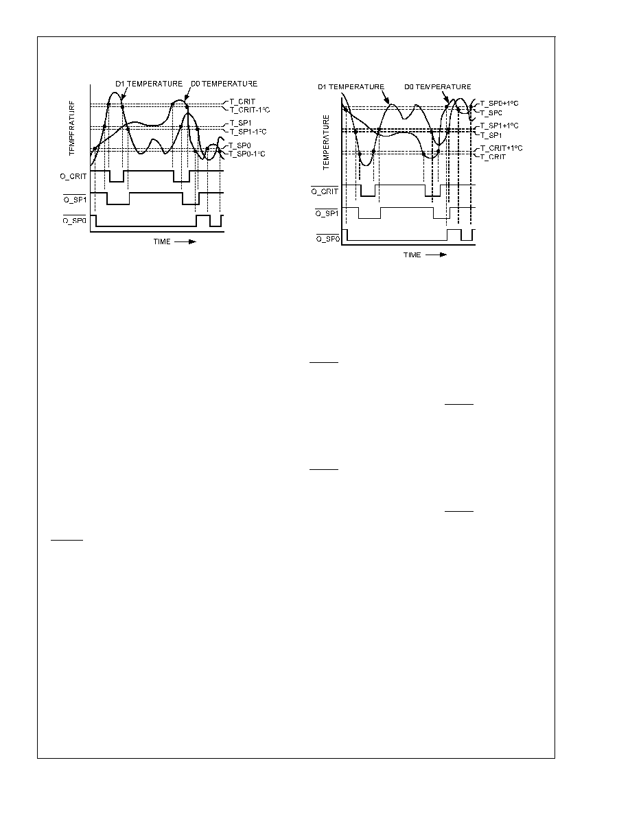
10132611
a) When programmed for a greater than comparison
10132612
b) When programmed for a less than comparison
FIGURE 2. Comparator output temperature response diagrams
LM88
www.national.com
5