 | –≠–ª–µ–∫—Ç—Ä–æ–Ω–Ω—ã–π –∫–æ–º–ø–æ–Ω–µ–Ω—Ç: LM9011 | –°–∫–∞—á–∞—Ç—å:  PDF PDF  ZIP ZIP |
LM9011
Electronic Ignition Interface
General Description
The LM9011 is an interface circuit which integrates the tim-
ing detection and logic control functions required for an auto-
motive electronic ignition system into one device.
A VRS interface is provided for crankshaft position informa-
tion via a toothed-wheel.
Four voltage comparators are provided for hardware diag-
nostics.
An electronic timing interface with output fault diagnostics is
provided to enable a micro-processor to drive an external
four channel ignition spark circuit.
The LM9011 is fully specified over the automotive tempera-
ture range of -40∞C to +125∞C, and is available in a 28 pin
Small Outline surface mount package.
Key Specifications
Features
n
Single 5V supply operation
n
VR Sensor Interface with dynamic hysteresis
n
Four Channel Electronic Timing spark driver with output
diagnostics
n
Electronic Timing Interface spark driver output voltage
from 5V to 16V
n
One Non-Inverting voltage comparator with hysteresis
n
Three Inverting voltage comparators with hysteresis
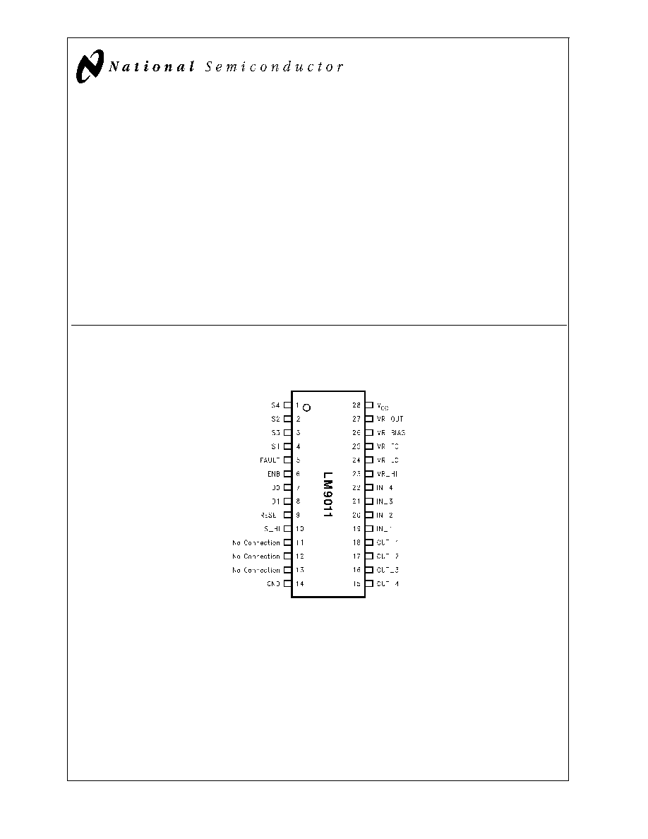
Connection Diagram
Top View
DS101264-1
Ordering Information LM9011M
See NS Package M28B
February 2000
LM901
1
Electronic
Ignition
Interface
© 2000 National Semiconductor Corporation
DS101264
www.national.com

Absolute Maximum Ratings
(Note 1)
Voltage
-0.3V to +7.0V
S_HI Voltage
-0.3V to 26.5V
VR_HI and VR_LO Inputs
+/-3mA
Comparator Inputs
-0.3V to +7.0V
Timing Interface Inputs
-0.3V to +7.0V
ESD Susceptibility (Note 3)
+/-2000V
Maximum Junction Temperature
150∞C
Storage Temperature Range
-65∞C to +150∞C
Lead Soldering Information:
Vapor Phase (60 Seconds)
215∞C
Infrared (15 Seconds)
220∞C
Operating Ratings
(Note 3)
V
CC
Voltage
4.75V to 5.25V
S_HI Voltage
V
CC
to 26V
Sx Outputs
-0.3V to S_HI +0.3V
Comparator Inputs
VR_HI and VR_LO Inputs
-0.3V to V
CC
+0.3V
+/-2.75mA
Timing Interface Inputs
-0.3V to V
CC
+0.3V
Thermal Resistances (M28B):
Junction to Case (
J-C)
15∞C/W
Junction to Ambient (
J-C)
69∞C/W
DC Electrical Characteristics
The following specifications apply for V
CC
= 5V, V
RESET
= V
CC
, V
S_HI
=
V
CC
, -40∞C
T
A
+125∞C, Application Circuit Figure 16, unless otherwise specified.
Symbol
Parameter
Conditions
Minimum
Maximum
Units
I
CC
Supply Current
RESET, IN_4 = V
CC
25
mA
ENB, D0, D1, IN_1, IN_2, IN_3 =
0V
VR_HI = +12.5µA
VR_LO = -12.5µA
Comparators
V
TH
1
Input Threshold
V
IN
_1 Decreasing from V
CC
to 0V
until V
OUT
_1
>
V
CC
/2
V
CC
X 0.435
V
CC
X 0.485
V
V
TH
2
Input Threshold
V
IN
_2 Decreasing from V
CC
to 0V
until V
OUT
_2
>
V
CC
/2
V
CC
X 0.435
V
CC
X 0.485
V
V
TH
3
Input Threshold
V
IN
_3 Decreasing from V
CC
to 0V
until V
OUT
_3
>
V
CC
/2
V
CC
X 0.40
V
CC
X 0.45
V
V
TH
4
Input Threshold
V
IN
_4 Decreasing from V
CC
to 0V
until V
OUT
_4
<
V
CC
/2
V
CC
X 0.45
V
CC
X 0.50
V
V
HYST
Input Hysteresis
All Comparators
150
400
mV
I
BIAS
Input Bias Current
IN_1, IN_2, IN_3 = 0V
V
IN
V
CC
IN_4 = 0V
V
IN
_4
V
CC
-1V
750
µA
V
OH
Output High Voltage
I
LOAD
= -100µAV
V
CC
-1
V
V
OL
Output Low Voltage
I
LOAD
= +100µAV
750
mV
VR Sensor Interface
V
OH
Output High Voltage
I
LOAD
= -15µA
VR_HI= -1mA, VR_LO = +1mA
V
CC
-1
V
V
OL
Output Low Voltage
Load = +15µA
VR_HI=+1mA, VR_LO = -1mA
750
mV
I
DIFF(MIN)
Minimum Detect Differential Input
Current (Note 4)
-40∞C
T
A
+25∞C
T
A
= +85∞C (Note 7)
T
A
= +125∞C
0.5
0.6
1.0
3.0
3.5
5.0
uA Pk-Pk
uA Pk-Pk
uA Pk-Pk
I
HYS
1
Input Hysteresis (Note 4)
I
DIFF
= 1mA pk-pk
75
250
uA Pk
I
HYS
2
Input Hysteresis (Note 4)
I
DIFF
= 2.5mA pk-pk
185
625
uA Pk
Electronic Timing Interface
V
IH
Input Logic 1 D0, D1, ENB,
RESET
V
CC
X 0.7
V
V
IL
Input Logic 0 D0, D1, ENB,
RESET
V
CC
X 0.3
V
I
IH
Input High Current Inputs D0, D1,
RESET
V
IN
= V
CC
10
µA
I
IH
Input High Current Input ENB
V
IN
= V
CC
125
µA
LM901
1
www.national.com
2
DC Electrical Characteristics
The following specifications apply for V
CC
= 5V, V
RESET
= V
CC
, V
S_HI
= V
CC
,
-40∞C
T
A
+125∞C, Application Circuit Figure 16, unless otherwise specified. (Continued)
Symbol
Parameter
Conditions
Minimum
Maximum
Units
Electronic Timing Interface
I
IL
Input Low Current Inputs D0, D1,
ENB
V
IN
= 0V
-10
µA
I
IL
Input Low Current Input RESET
V
IN
= 0V
-125
µA
V
OH
Output High Voltage Outputs S1,
S2, S3, S4
I
LOAD
= -10mA, V
S_HI
= 5V
3.75
V
V
OL
Output Low Voltage Outputs S1,
S2, S3, S4
I
LOAD
= 1mA, V
S_ HI
= 5V
300
mV
V
OH
Output High Voltage Outputs S1,
S2, S3, S4
I
LOAD
= -10mA, V
S_HI
= 16V
14
V
V
OL
Output Low Voltage Outputs S1,
S2, S3, S4
I
LOAD
= 1mA, V
S_HI
=16V
450
mV
V
OH
Output High Voltage Outputs S1,
S2, S3, S4
I
LOAD
= -10mA, V
S_HI
=26V
22
V
V
OL
Output Low Voltage Outputs S1,
S2, S3, S4
I
LOAD
= 1mA, V
S_HI
=26V
600
mV
V
OH
FAULT Pin Output High Voltage
I
FAULT
= -100µA, no fault
V
CC
-1
V
V
OL
FAULT Pin Output Low Voltage
I
FAULT
= 100µA, any fault
750
mV
V
FAULT
Fault Treshold Voltage Outputs
S1, S2, S3, S4
Sx Output Short Fault
V
CC
X 0.2
V
CC
X 0.5
V
I
FOL
TRI-STATE Output Current
Outputs S1, S2, S3, S4
V
RESET
= 0V, V
S _HI
= 5V
R
LOAD
= 10K
-12
-50
µA
AC Electrical Characteristics
The following specifications apply for V
CC
= 5V, V
S_HI
= V
CC
, V
RESET
= V
CC
, -40∞C
T
A
+125∞C. The AC Timing Characteristics
are not production tested. Minimum and Maximum limits are guaranteed by device characterization.
Symbol
Parameter
Conditions
Minimum
Maximum
Units
Comparators
T
RISE
Output Rise Time
10% to 90%, C
LOAD
= 25pF
5
µs
T
FALL
Output Fall Time
90% to10%, C
LOAD
= 25pF
5
µs
VR Sensor Interface (Note 4)
T
RISE
Output Rise Time
10% to 90%, C
LOAD
= 100pF,
R
LOAD
= 100K
10
µs
T
FALL
Output Fall Time
90% to10%, C
LOAD
= 100pF,
R
LOAD
= 100k
5
ms
T
DELAY
Zero Crossing Delay Time (Note
6)
I
DIFF
= 5µA pk-pk, F
VRS
= 200Hz
I
DIFF
= 50µA pk-pk, F
VRS
=
2.5KHz
1
10
ms
ms
F
MAX
Maximum VRS Frequency
C
LOAD
= 100pF, R
LOAD
= 100K
I
DIFF
= 5µA pk-pk
50
KHz
Electronic Timing Interface
T
RISE
1
Sx Output Rise Time
Sx Rises10% to 90%
C
LOAD
= 6.8nF, R
LOAD
= 10K
5
µs
C
LOAD
= 12.7nF, R
LOAD
= 10K
8
µs
T
FALL
1
Sx Output Fall Time
Sx Falls 90% to 10%
C
LOAD
= 6.8nF, R
LOAD
= 10K
15
µs
C
LOAD
= 12.7nF, R
LOAD
= 10K
25
µs
T
SETUP
SetupTime (Notes 7, 8 and 9)
1
µs
T
HOLD
Hold Time
0.5
µs
LM901
1
www.national.com
3
AC Electrical Characteristics
(Continued)
The following specifications apply for V
CC
= 5V, V
S_HI
= V
CC
, V
RESET
= V
CC
, -40∞C
T
A
+125∞C. The AC Timing Characteristics
are not production tested. Minimum and Maximum limits are guaranteed by device characterization.
Symbol
Parameter
Conditions
Minimum
Maximum
Units
Electronic Timing Interface
T
DF
1
Fault Delay Time
Sx Output Short to Ground Fault
From ENB = 1 to FAULT
10%
C
FAULT
= 25pF
2
µs
T
DF
2
Fault Delay Time
Sx Output Short to Battery Fault
From ENB = 0 to FAULT
10%
C
FAULT
= 25pF
2
µs
T
TRI
TRI-STATE Delay Time
From RESET = 0 to All Sx
Outputs Off
2
µs
T
RISE
2
Fault Pin Rise Time
10% to 90%, C
FAULT
= 25pF
5
µs
T
FF(OFF)
False Fault Time
From ENB = 0 to FAULT
90%
C
FAULT
= 25pF
C
LOAD
= 6.8nF, R
LOAD
= 10K
25
µs
C
LOAD
= 12.7nF, R
LOAD
= 10K
30
µs
T
FF(ON)
False Fault Time
From ENB = 1 to FAULT
90%
C
FAULT
= 25pF
C
LOAD
= 6.8nF, R
LOAD
= 10K
8
µs
C
LOAD
= 12.7, R
LOAD
= 10K
10
µs
T
UDF
Undefined Fault Time
From ENB = 0 for 8uSec, to Valid
FAULT
C
LOAD
= 6.8nF, R
LOAD
= 10K
20
µs
C
LOAD
= 12.7nF, R
LOAD
= 10K
25
µs
Note 1: Absolute Maximum Ratings indicate the limits beyond which damage may occur.
Note 2: ESD Ratings is with Human Body Model: 100pF discharged through a 1500
resistor.
Note 3: Operating ratings indicate conditions for which the device is intended to be functional, but may not meet the guaranteed specific performance limits. For guar-
anteed specifications and conditions, see the Electrical Characteristics.
Note 4: Tested per VR Sensor Interface test circuit. See figures 8 and 9.
Note 5: Minimum Detect Current is not production tested at +85C. Specifications is guaranteed through device characterization and Test Limits at 25∞C and 125∞C.
Note 6: VR Sensor Interface Tdelay, measured from VR input sine wave zero-crossing to VR_OUT going high. See figure 9.
Note 7: Electronic Timing Interface Tsetup, minimum time between Vcc
>
4.75V and RESET = 1.
Note 8: Electronic Timing Interface Tsetup, minimum time between RESET = 1 and D0 = 1.
Note 9: Electronic Timing Interface Tsetup, minimum time between D0 / D1 = valid and ENB = 1.
LM901
1
www.national.com
4
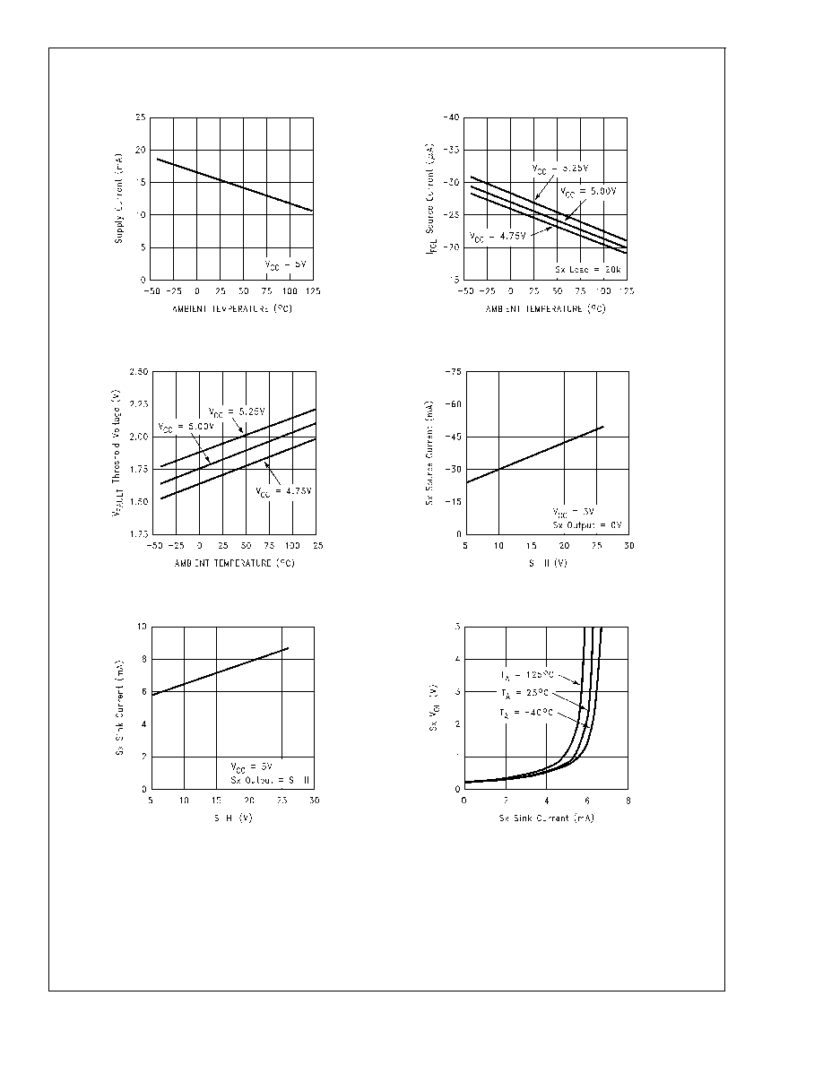
Typical Performance Characteristics
Supply Current vs Temperature
DS101264-3
Ifol Source Current vs Temperature
DS101264-4
VFault Threshold vs Temperature
DS101264-5
Sx Source Current vs S_HI Voltage
DS101264-6
Sx Sink Current vs S_HI Voltage
DS101264-7
Sx Vol vs Sx Sink Current
DS101264-8
LM901
1
www.national.com
5