 | –≠–ª–µ–∫—Ç—Ä–æ–Ω–Ω—ã–π –∫–æ–º–ø–æ–Ω–µ–Ω—Ç: LM9040 | –°–∫–∞—á–∞—Ç—å:  PDF PDF  ZIP ZIP |
TL H 12372
LM9040
Dual
Lambda
Sensor
Interface
Amplifier
August 1995
LM9040
Dual Lambda Sensor Interface Amplifier
General Description
The LM9040 is a dual sensor interface circuit consisting of
two independent sampled input differential amplifiers de-
signed for use with conventional Lambda Oxygen Sensors
The Lambda Sensor is used for monitoring the oxygen con-
centration in the exhaust of gasoline engines using catalytic
after treatment and will deliver a voltage signal which is de-
pendent on the air-fuel mixture The gain of the amplifiers
are internally set and can directly convert the Lambda sen-
sor output voltage to a level suitable for A D conversion in a
system using a 5V reference
The input common mode voltage range of each amplifier is
g
2V with respect to the IC ground pin This will allow the IC
to connect to sensors which are remotely grounded at the
engine exhaust manifold or exhaust pipe
Each amplifier is capable of independent default operation
should either or both of the leads to a sensor become
open circuited
Noise filtering is provided by an internal switched capacitor
low pass filter as part of each amplifier and by external
components
The LM9040 is fully specified over the automotive tempera-
ture range of
b
40 C to
a
125 C and is provided in a 14-pin
Small Outline surface mount package
Features
Y
Single 5V supply operation
Y
Common mode input voltage range of
g
2V
Y
Differential input voltage range of 50 mV to 950 mV
Y
Sampled differential input
Y
Switched capacitor low pass filter
Y
Internal oscillator and V
BB
generator
Y
Open input default operation
Y
Cold sensor default operation
Y
Low power consumption (42 mW max)
Y
Gain set by design and guaranteed over the operating
temperature range
Applications
Y
Closed loop emissions control
Y
Catalytic converter monitoring
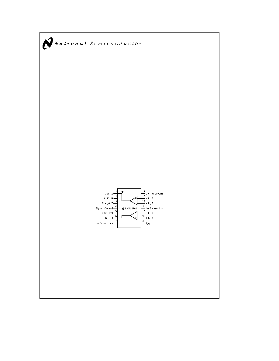
Connection Diagram
TL H 12372 ≠ 1
Top View
Ordering Information
LM9040M
See NS Package Number M14B
C1995 National Semiconductor Corporation
RRD-B30M115 Printed in U S A
Absolute Maximum Ratings
If Military Aerospace specified devices are required
please contact the National Semiconductor Sales
Office Distributors for availability and specifications
Supply Voltage
b
0 3V to
a
6 0V
Input Voltage Continuous (Note 1)
g
14V
Input Voltage Transient t
s
1 ms (Note 1)
g
60V
ESD Susceptibility (Note 2)
g
2000V
Maximum Junction Temperature
150 C
Storage Temperature Range
b
65 C to
a
150 C
Lead Soldering Information
Vapor Phase (60 Seconds)
215 C
Infrared (15 Seconds)
220 C
Operating Ratings
Supply Voltage
4 75V to 5 25V
Differential Input Voltage
0V to
a
1V
Common Mode Voltage
g
2V
Power Dissipation
42 mW
DC Electrical Characteristics
The following specifications apply for V
CC
e
5 0V V
DIFF
e
500 mV V
CM
e
0V R
OSC
e
178 kX
b
40 C
s
T
A
s
a
125 C DC
Test Circuit
Figure 1 unless otherwise specified
Symbol
Parameter
Conditions
Min
Max
Units
I
CC
Supply Current
4 75V
s
V
CC
s
5 25V
8 0
mA
Z
DIFF
Differential Input Impedance
4 75V
s
V
CC
s
5 25V
1 05
1 60
Meg X
Z
IO
Inverting Input to Ground Impedance
Non-Inverting Inputs Open
10 00
Meg X
V
OL
Output Low Voltage
V
DIFF
e
0V I
LOAD
e
2 0 mA
100
mV
V
OC
V
OUT
Center
One or Both Input(s) Open
V
CC
0 380
V
CC
0 425
V
4 75V
s
V
CC
s
5 25V
V
OUT(ERROR)
(V
OUT
) ≠ (V
DIFF
4 53)
50 mV
s
V
DIFF
s
950 mV V
CM
e
0V
g
65
mV
V
OH
Output High Voltage
V
DIFF
e
5V I
LOAD
e b
2 mA
V
CC
b
0 1V
V
R
OUT
Output Resistance
1500
3500
X
CMRR
(DC)
DC Common Mode Error
b
2V
s
V
CM
s
a
2V
g
4 5
mV V
T
RISE
Output Rise Time
C
OUT
e
0 01 mF
1 2
ms
T
FALL
Output Fall Time
C
OUT
e
0 01 mF
1 2
ms
F
C
Low Pass Filter
b
3 dB
C
OUT
e
0 01 mF
400
700
Hz
Note 1
The input voltage must be applied through external 4 kX input resistors See
Figure 2 AC Test Circuit Amplifier operation will be disrupted but will not be
destructive
Note 2
ESD rating is with Human Body Model 100 pF discharged through a 1500X resistor
TL H 12372 ≠ 2
FIGURE 1 DC Test Circuit
TL H 12372 ≠ 3
FIGURE 2 AC Test Circuit
2
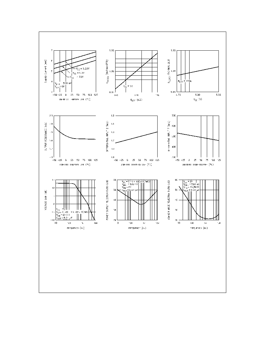
Typical Performance Characteristics
Supply Current vs Temperature
TL H 12372 ≠ 4
F
CLOCK
(Normalized) vs R
OSC
TL H 12372 ≠ 5
F
CLOCK
(Normalized) vs V
CC
TL H 12372 ≠ 6
Output R vs Temperature
TL H 12372 ≠ 7
Z
DIFF
vs Temperature
TL H 12372 ≠ 8
F
C
vs Temperature
TL H 12372 ≠ 9
Voltage Gain vs Frequency
TL H 12372 ≠ 10
PSRR vs Frequency
TL H 12372 ≠ 11
CMRR vs Frequency
TL H 12372 ≠ 12
3
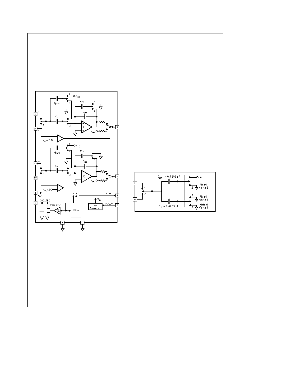
Circuit Description
The LM9040 is fabricated in CMOS technology and is de-
signed to operate from a single well regulated 5V supply
The IC consists of two independent differential amplifiers
which are designed using two-phased switched capacitor
networks (SCN) The differential inputs have a common
mode operating range of 2V above and below ground The
SCN includes the input sampling the lowpass filter cold
sensor bias voltage and the gain circuitry Each amplifier
has an independent voltage comparator to detect an open
inverting input pin Additional support circuitry includes the
oscillator clock generator and V
BB
bias generator
TL H 12372 ≠ 13
FIGURE 3 Simplified Circuit
Oscillator
The device contains an internal oscillator which is used to
drive the internal two-phase clock generator The oscillator
requires an external resistor value of 178 kX from the
``OSC
RES'' pin to device V
CC
This resistor value deter-
mines the charge rate of the internal capacitor and thus
sets the oscillator frequency The internal oscillator capaci-
tor is matched to the switched capacitor networks so that
the absolute capacitance values are not as important as is
the absolute ratios of the capacitors The oscillator frequen-
cy is approximately 200 kHz
The oscillator resistor should be located as close to the
OSC
RES pin as possible Any variation of the oscillator
resistor value any stray capacitance on the OSC
RES pin
or any changes in the supply voltage will result in a change
in the oscillator frequency This will directly affect the device
Differential Input Impedance and Low Pass filter response
Additional circuitry takes the oscillator signal and generates
two non-overlapping clock signals and a CLK
OUT signal
The clock signals operate at one half the oscillator frequen-
cy or typically 100 kHz This results in a Nyquist frequency
of typically 50 kHz
Clock Out Clock In
For the input stage to work with common mode voltages
below Ground potential a negative bias voltage (V
BB
) is
needed The CLK
OUT pin is used to provide the AC sig-
nal needed to drive the internal V
BB
bias generator through
an external coupling capacitor A minimum coupling capaci-
tor value of 100 pF to a maximum value of 0 1 mF is recom-
mended The CLK
IN pin is the input to the V
BB
bias gen-
erator circuitry
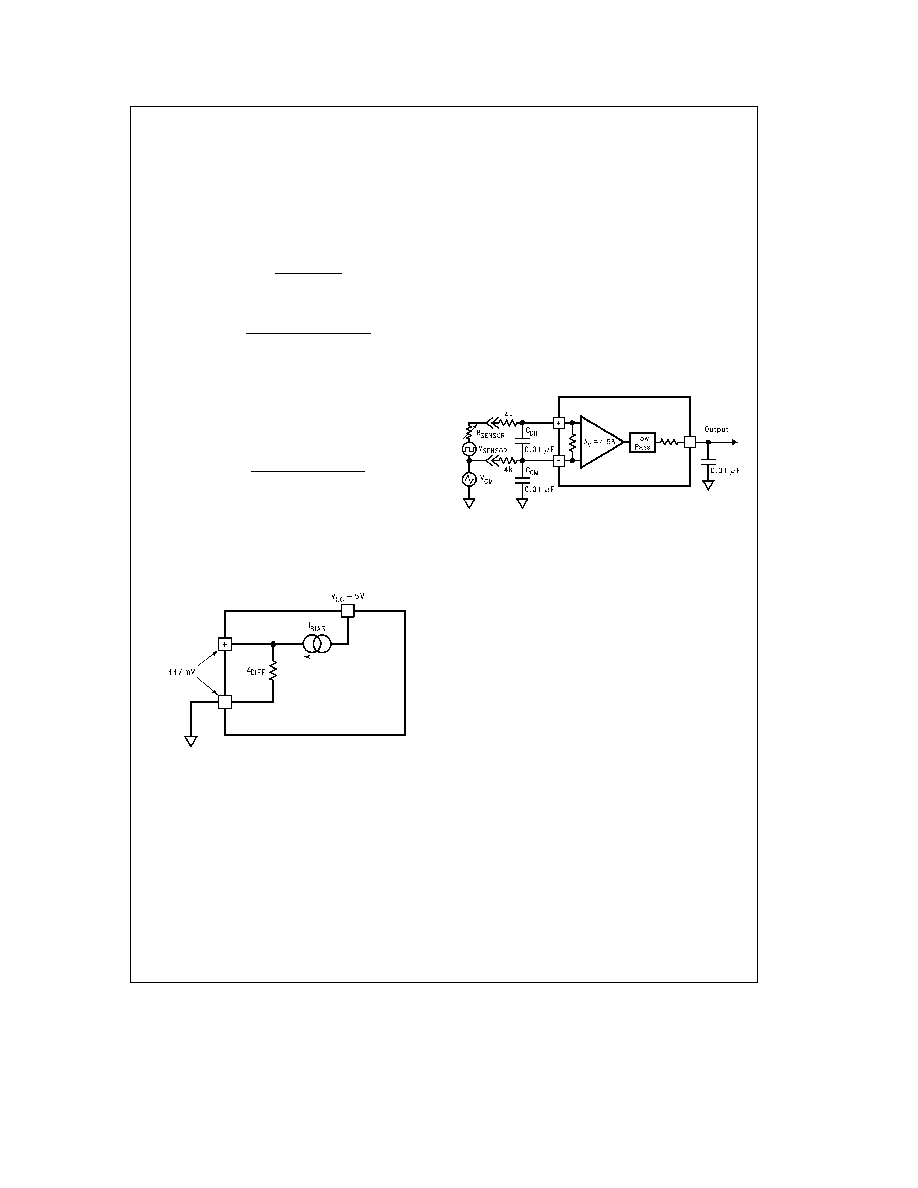
Differential Input Circuit
The input stage can be best described as a switched Sam-
ple and Difference circuit (see
Figure 4 ) When the input
capacitor C
IN
is switched to the non-inverting input the in-
put voltage plus the common mode voltage is stored on C
IN
When C
IN
is switched to the inverting input C
IN
will be dis-
charged by an amount equal to the common mode voltage
The remaining charge across C
IN
will be equal to the differ-
ential input voltage and a proportional charge will be trans-
ferred through the virtual ground via the gain stage
TL H 12372 ≠ 14
FIGURE 4 Simplified Switched Capacitor Input Circuit
4
Differential Input Circuit
(Continued)
The differential input impedance is a function of the value of
the input capacitor array and the sampling frequency The
capacitor C
BIAS
is used to generate a bias voltage across
the Differential Input impedance (Z
DIFF
) This bias voltage is
similar to the Lambda Sensor output voltage at the stoichio-
metric air-fuel mixture (l
e
1) The bias voltage is set by the
ratio of C
IN
and C
BIAS
and the value of V
CC
The resulting bias voltage across the Differential Input is
defined as
V
BIAS
e
V
CC
C
BIAS
(C
IN
a
C
BIAS
)
With C
BIAS
e
0 7286 pF C
IN
e
7 421 pF F
CLOCK
e
100 kHz and V
CC
e
5V
V
BIAS
e
5
7 286E-13
(7 4213E-12
a
7 286E-13)
V
BIAS
e
447 mV
In effect the result is the same as forcing a bias current
through the Differential Input impedance
The bias current is defined as
I
BIAS
e
V
CC
C
BIAS
F
CLOCK
I
BIAS
e
364 3 nA
The Differential Input impedance is defined as
Z
DIFF
e
1
(C
IN
a
C
BIAS
)
F
CLOCK
Z
DIFF
e
1 227 MX
This bias voltage will be developed across the Differential
Input impedance (Z
DIFF
) if there is no other path available
from the non-inverting input pin for I
BIAS
and the inverting
input has a current path to ground See
Figure 5 During
normal operating conditions I
BIAS
will have a negligible ef-
fect on accuracy
TL H 12372 ≠ 15
FIGURE 5 Equivalent Input Bias Circuit
Differential Input Filtering
Since each input is sampled independently an anti-aliasing
filter is required at the amplifier inputs to ensure that the
input signal does not exceed the Nyquist frequency
This external low-pass filter is implemented by adding a ca-
pacitor (C
DIFF
) across the differential input See
Figure 6
This forms an RC network across the differential inputs in
conjunction with the required external 4 kX resistors and
the differential input impedance (Z
DIFF
) The capacitor se-
lected should be small enough to have minimal effect on
gain accuracy in the application yet large enough to filter
out unwanted noise Given that the F
C
of the LM9040 is
typically 500 Hz the use of a 0 01 mF capacitor will general-
ly provide adequate filtering with less than
b
0 4 dB of input
attenuation at 500 Hz and approximately
b
28 dB at 50 kHz
A larger value capacitor can be used if needed but a value
larger than typically 0 02 mF will begin to dominate the cut-
off frequency of the application This capacitor must be a
low leakage and low ESR type so that circuit performance is
not degraded
TL H 12372 ≠ 16
FIGURE 6 Differential and Common Mode Filtering
Common Mode Filtering
The differential input sampling of the LM9040 actually re-
duces the effects of common mode input noise at low fre-
quencies The time interval between the sampling of the
inverting input and the non-inverting input is one half of a
clock period A change in the common mode voltage during
this short time interval can cause an error in the charge
stored on C
IN
This will result in an error seen on the output
voltage For a sine-wave common mode voltage the mini-
mum common mode rejection is
CMRR
e
2
q
F
CMR
(0 5 F
CLOCK
)
4 53
Where F
CMR
is the frequency of the common mode signal
and F
CLOCK
is the clock frequency
5