LM9040
Dual Lambda Sensor Interface Amplifier
General Description
The LM9040 is a dual sensor interface circuit consisting of
two independent sampled input differential amplifiers de-
signed for use with conventional Lambda Oxygen Sensors.
The Lambda Sensor is used for monitoring the oxygen con-
centration in the exhaust of gasoline engines using catalytic
after treatment and will deliver a voltage signal which is
dependent on the air-fuel mixture. The gain of the amplifiers
are internally set and can directly convert the Lambda sen-
sor output voltage to a level suitable for A/D conversion in a
system using a 5V reference.
The input common mode voltage range of each amplifier is
±
2V with respect to the IC ground pin. This will allow the IC
to connect to sensors which are remotely grounded at the
engine exhaust manifold or exhaust pipe.
Each amplifier is capable of independent default operation
should either, or both, of the leads to a sensor become open
circuited.
Noise filtering is provided by an internal switched capacitor
low pass filter as part of each amplifier, and by external
components.
The LM9040 is fully specified over the automotive tempera-
ture range of -40°C to +125°C and is provided in a 14-pin
Small Outline surface mount package.
Features
n
Single 5V supply operation
n
Common mode input voltage range of
±
2V
n
Differential input voltage range of 50 mV to 950 mV
n
Sampled differential input
n
Switched capacitor low pass filter
n
Internal oscillator and V
BB
generator
n
Open input default operation
n
Cold sensor default operation
n
Low power consumption (42 mW max)
n
Gain set by design and guaranteed over the operating
temperature range
Applications
n
Closed loop emissions control
n
Catalytic converter monitoring
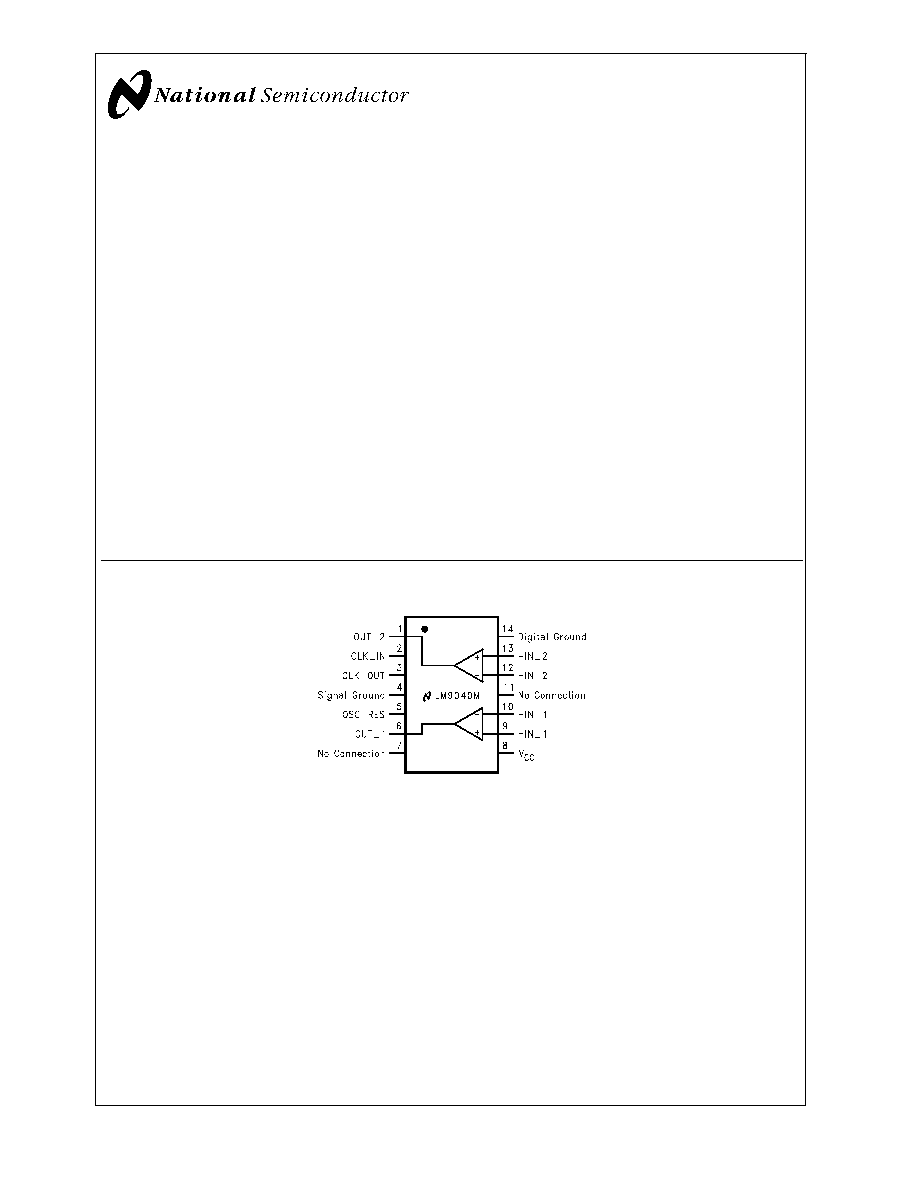
Connection Diagram
01237201
Top View
Ordering Information
LM9040M
See NS Package Number M14B
November 2001
LM9040
Dual
Lambda
Sensor
Interface
Amplifier
© 2001 National Semiconductor Corporation
DS012372
www.national.com
Absolute Maximum Ratings
(Note 1)
If Military/Aerospace specified devices are required,
please contact the National Semiconductor Sales Office/
Distributors for availability and specifications.
Supply Voltage
-0.3V to +6.0V
Input Voltage Continuous (Note 2)
±
14V
Input Voltage Transient t
1 ms (Note 2)
±
60V
ESD Susceptibility (Note 3)
±
2000V
Maximum Junction Temperature
150°C
Storage Temperature Range
-65°C to +150°C
Lead Soldering Information
Vapor Phase (60 Seconds)
215°C
Infrared (15 Seconds)
220°C
Operating Ratings
Supply Voltage
4.75V to 5.25V
Differential Input Voltage
0V to +1V
Common Mode Voltage
±
2V
Power Dissipation
42 mW
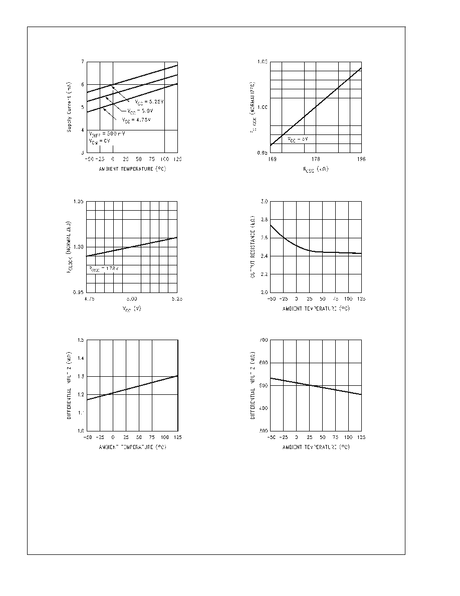
DC Electrical Characteristics
The following specifications apply for V
CC
= 5.0V, V
DIFF
= 500 mV, V
CM
= 0V, R
OSC
= 178 k
, -40°C
T
A
+125°C, DC Test
Circuit
Figure 1, unless otherwise specified.
Symbol
Parameter
Conditions
Min
Max
Units
I
CC
Supply Current
4.75V
V
CC
5.25V
8.0
mA
Z
DIFF
Differential Input Impedance
4.75V
V
CC
5.25V
1.05
1.60
Meg
Z
IO
Inverting Input to Ground Impedance
Non-Inverting Inputs Open
10.00
Meg
V
OL
Output Low Voltage
V
DIFF
= 0V, I
LOAD
= 2.0 µA
100
mV
V
OC
V
OUT
Center
One, or Both, Input(s) Open
4.75V
V
CC
5.25V
V
CC
·
0.380
V
CC
·
0.425
V
V
OUT(ERROR)
(V
OUT
)-(V
DIFF
·
4.53)
50 mV
V
DIFF
950 mV, V
CM
= 0V
±
65
mV
V
OH
Output High Voltage
V
DIFF
= 5V, I
LOAD
= -2 µA
V
CC
- 0.1V
V
R
OUT
Output Resistance
1500
3500
CMRR
(DC)
DC Common Mode Error
-2V
V
CM
+2V
±
4.5
mV/V
T
RISE
Output Rise Time
C
OUT
= 0.01 µF
1.2
ms
T
FALL
Output Fall Time
C
OUT
= 0.01 µF
1.2
ms
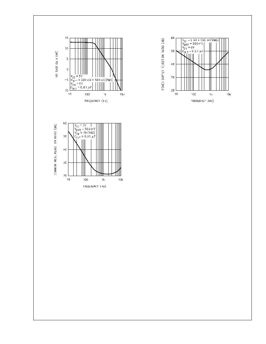
F
C
Low Pass Filter -3 dB
C
OUT
= 0.01 µF
400
700
Hz
Note 1: Absolute Maximum Ratings indicate limits beyond which damage to the device may occur.
Note 2: The input voltage must be applied through external 4 k
input resistors. See
Figure 2
, AC Test Circuit. Amplifier operation will be disrupted, but will not be
destructive.
Note 3: ESD Rating is with Human Body Model: 100 pF discharged through a 1500
resistor.
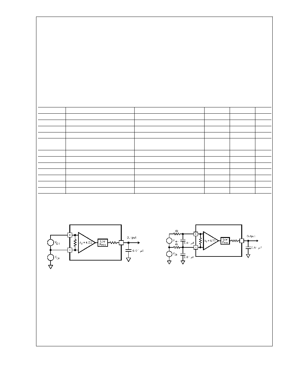
01237202
FIGURE 1. DC Test Circuit
01237203
FIGURE 2. AC Test Circuit
LM9040
www.national.com
2
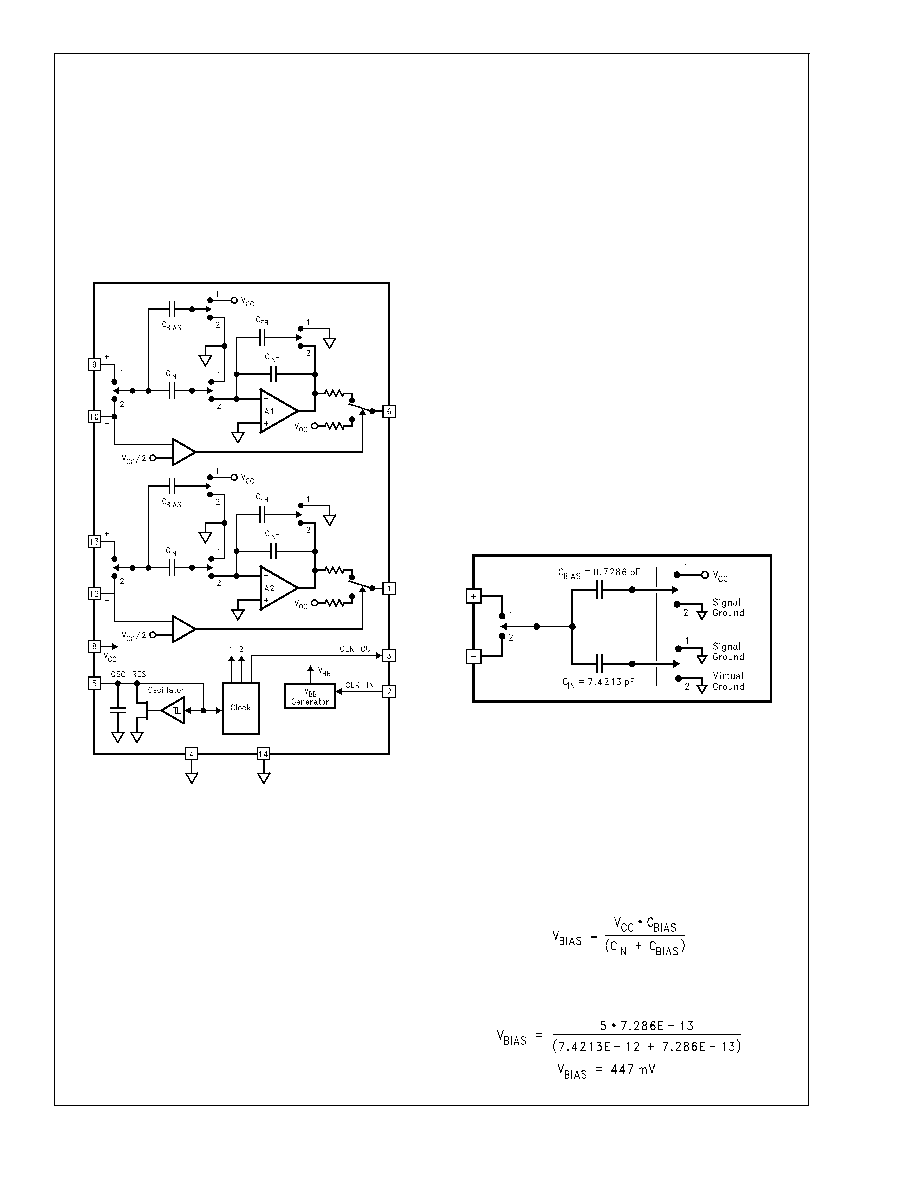
Circuit Description
The LM9040 is fabricated in CMOS technology and is de-
signed to operate from a single, well regulated, 5V supply.
The IC consists of two independent differential amplifiers
which are designed using two-phased switched capacitor
networks (SCN). The differential inputs have a common
mode operating range of 2V above and below ground. The
SCN includes the input sampling, the lowpass filter, cold
sensor bias voltage, and the gain circuitry. Each amplifier
has an independent voltage comparator to detect an open
inverting input pin. Additional support circuitry includes the
oscillator, clock generator, and V
BB
bias generator.
Oscillator
The device contains an internal oscillator which is used to
drive the internal two-phase clock generator. The oscillator
requires an external resistor value of 178 k
from the
"OSC_RES" pin to device V
CC
. This resistor value deter-
mines the charge rate of the internal capacitor, and thus sets
the oscillator frequency. The internal oscillator capacitor is
matched to the switched capacitor networks, so that the
absolute capacitance values are not as important as is the
absolute ratios of the capacitors. The oscillator frequency is
approximately 200 kHz.
The oscillator resistor should be located as close to the
OSC_RES pin as possible. Any variation of the oscillator
resistor value, any stray capacitance on the OSC_RES pin,
or any changes in the supply voltage, will result in a change
in the oscillator frequency. This will directly affect the device
Differential Input Impedance, and Low Pass filter response.
Additional circuitry takes the oscillator signal and generates
two non-overlapping clock signals, and a CLK_OUT signal.
The clock signals operate at one half the oscillator fre-
quency, or typically 100 kHz. This results in a Nyquist fre-
quency of typically 50 kHz.
Clock Out/Clock In
For the input stage to work with common mode voltages
below Ground potential, a negative bias voltage (V
BB
) is
needed. The CLK_OUT pin is used to provide the AC signal
needed to drive the internal V
BB
bias generator through an
external coupling capacitor. A minimum coupling capacitor
value of 100 pF to a maximum value of 0.1 µF is recom-
mended. The CLK_IN pin is the input to the V
BB
bias gen-
erator circuitry.
Differential Input Circuit
The input stage can be best described as a switched Sample
and Difference circuit (see
Figure 4). When the input capaci-
tor C
IN
is switched to the non-inverting input, the input volt-
age plus the common mode voltage is stored on C
IN
. When
C
IN
is switched to the inverting input, C
IN
will be discharged
by an amount equal to the common mode voltage. The
remaining charge across C
IN
will be equal to the differential
input voltage, and a proportional charge will be transferred
through the virtual ground via the gain stage.
The differential input impedance is a function of the value of
the input capacitor array and the sampling frequency. The
capacitor C
BIAS
is used to generate a bias voltage across the
Differential Input Impedance (Z
DIFF
). This bias voltage is
similar to the Lambda Sensor output voltage at the stoichio-
metric air-fuel mixture (
= 1). The bias voltage is set by the
ratio of C
IN
and C
BIAS
, and the value of V
CC
.
The resulting bias voltage across the Differential Input is
defined as:
With C
BIAS
= 0.7286 pF, C
IN
= 7.421 pF, F
CLOCK
= 100 kHz,
and V
CC
= 5V:
01237213
FIGURE 3. Simplified Circuit
01237214
FIGURE 4. Simplified Switched Capacitor Input Circuit
LM9040
www.national.com
5