LM9076
150mA Ultra-Low Quiescent Current LDO Regulator with
Delayed Reset Output
General Description
The LM9076 is a 5 Volt, +/-2%, 150mA logic controlled
voltage regulator. The regulator features an active low de-
layed reset output flag which can be used to reset a micro-
processor system at turn-ON and in the event that the regu-
lator input voltage falls below a minimum value. An external
capacitor programs a delay time interval before the reset
output pin can return high.
Designed for automotive and industrial applications, the
LM9076 contains a variety of protection features such as
thermal shutdown, input transient protection and a wide
operating temperature range. The LM9076 uses an PNP
pass transistor which allows low drop-out voltage operation.
Features
n
Ultra Low Ground Pin Current, 25µA typical for 100µA
load
n
V
OUT
initial accuracy of +/-1%
n
V
OUT
accurate to +/2% over Load and Temperature
Conditions
n
Low Dropout Voltage, 200mV typical with 150mA load
n
Low Off State Ground Pin current
n
Delayed RESET output pin for low V
OUT
detection
n
+70V/-50V Voltage Transients
n
Operational V
IN
up to +40V
Typical Application
20083030
Package Outline
20083027
Top View
Part Number LM9076S≠5.0
See NS TO-263 Package Number TS5
20083028
Top View
Part Number LM9076BMA≠5.0
See NS SOIC Package Number M08A
December 2003
LM9076
-
150mA
Ultra-Low
Quiescent
Current
LDO
Regulator
with
Delayed
Reset
Output
© 2003 National Semiconductor Corporation
DS200830
www.national.com
Absolute Maximum Ratings
(Note 1)
V
IN
(DC)
-15V to +55V
V
IN
(+Transient) t
<
10ms, Duty Cycle
<
1% +70V
V
IN
(-Transient) t
<
1ms, Duty Cycle
<
1%
-50V
SHUTDOWN Pin
-15V to +52V
RESET Pin
-0.3V to 20V
C
DELAY
Pin
-0.3V to V
OUT
+0.3V
Storage Temperature
-65∞C to +150∞C
Junction Temperature (T
J
)
+175C
ESD, HBM, per AEC - Q100 - 002
+/-2kV
ESD, MM, per AEC - Q100 - 003
+/-250V
Operating Ratings
(Note 1)
V
IN
Pin
5.35V to 40V
V
SHUTDOWN
Pin
0V to 40V
Ambient Temperature
-40∞C
<
T
A
<
+125∞C
Thermal Resistance TS5B (Note 6)
ja
75∞C/W
jc
2.9∞C/W
Thermal Resistance M08A (Note 6)
ja
156∞C/W
jc
59∞C/W
Electrical Characteristics for LM9076≠5.0
The following specifications apply for V
IN
= 14V; V
SHUTDOWN
= Open; I
LOAD
= 10mA; T
A
= +25∞C; C
OUT
= 10µF, 0.5
<
ESR
<
4.0
; unless otherwise specified. Bold Values indicate -40∞C T
A
125∞C. (Note 4, Note 5)
Symbol
Parameter
Conditions
Min
Typ
Max
Units
LM9076≠5.0 REGULATOR CHARACTERISTICS
V
OUT
Output Voltage
4.95
5.00
5.05
V
1mA
I
LOAD
150mA
4.90
5.00
5.10
V
V
IN
= 60V,
R
LOAD
= 1K
, t
40ms
4.50
5.00
5.50
V
Output Voltage Off
V
SHUTDOWN
2V,
R
LOAD
= 1K
≠
40
250
mV
Reverse Battery
V
IN
= -15V,
R
LOAD
= 1K
≠
0
≠300
mV
V
OUT
Line Regulation
9.0V
V
IN
16V,
I
LOAD
= 10mA
≠
4
25
mV
16V
V
IN
40V,
I
LOAD
= 10mA
≠
17
25
mV
Load Regulation
1mA
I
LOAD
150mA
≠
42
60
mV
V
DO
Dropout Voltage
I
LOAD
= 10mA
≠
30
50
mV
I
LOAD
= 50mA
≠
80
≠
mV
I
LOAD
= 150mA
≠
150
250
mV
I
GND
Ground Pin Current
9V
V
IN
16V,
I
LOAD
= 100uA
≠
25
35
µA
9V
V
IN
40V,
I
LOAD
= 10mA
≠
125
160
µA
9V
V
IN
40V,
I
LOAD
= 50mA
≠
0.6
≠
mA
9V
V
IN
16V,
I
LOAD
= 150mA
≠
3.6
4.5
mA
Ground Pin Current
in Shut- down Mode
9V
V
IN
40V,
V
SHUTDOWN
= 2V
≠
15
25
µA
I
SC
V
OUT
Short Circuit
Current
V
IN
= 14V,
R
LOAD
= 1
200
400
750
mA
PSRR
Ripple Rejection
V
IN
= (14V
DC
) +
(1V
RMS
@
120Hz)
I
LOAD
= 50mA
50
60
≠
dB
RESET PIN CHARACTERISTICS
V
OR
Minimum V
IN
for valid
RESET Status
(Note 3)
≠
1.3
2.0
V
LM9076
www.national.com
2
Electrical Characteristics for LM9076≠5.0
(Continued)
The following specifications apply for V
IN
= 14V; V
SHUTDOWN
= Open; I
LOAD
= 10mA; T
A
= +25∞C; C
OUT
= 10µF, 0.5
<
ESR
<
4.0
; unless otherwise specified. Bold Values indicate -40∞C T
A
125∞C. (Note 4, Note 5)
Symbol
Parameter
Conditions
Min
Typ
Max
Units
RESET PIN CHARACTERISTICS
V
THR
V
OUT
Threshold for
RESET Low
(Note 3)
0.83
0.89
0.94
X V
OUT
(Nom)
V
OH
RESET pin high
voltage
External pull-up
resistor to V
OUT
=
100k
V
OUT
X 0.90
V
OUT
X 0.99
V
OUT
V
V
OL
RESET pin low
voltage
C
DELAY
<
4.0V,
I
SINK
= 250µA
≠
0.2
0.3
V
C
DELAY
PIN CHARACTERISTICS
I
DELAY
C
DELAY
Charging
Current
V
IN
= 14V,
V
DELAY
= 0V
-0.35
-0.42
-0.50
uA
V
OL
C
DELAY
pin low
voltage
V
OUT
<
4.0V,
I
SINK
= I
DELAY
--
0.100
--
V
t
DELAY
Reset Delay Time
V
IN
= 14V, C
DELAY
=
0.001uF
V
OUT
rising from 0V,
t from V
OUT
>
V
OR
to RESET pin HIGH
9.5
11.9
14.3
ms
SHUTDOWN CONTROL LOGIC -- LM9076BMA Only
V
IL(SD)
SHUTDOWN Input
Low Threshold
Voltage
V
SHUTDOWN
pin falling
from 5.0V until Vout
>
4.5V (Vout = On)
1
1.5
--
V
V
IH(SD)
SHUTDOWN Input
High Threshold
Voltage
V
SHUTDOWN
pin rising
from 0V until Vout
<
0.5V (Vout = Off)
--
1.5
2
V
I
IH(SD)
SHUTDOWN Pin
High Bias Current
V
SHUTDOWN
= 40V
--
35
µA
V
SHUTDOWN
= 5V
--
15
35
µA
V
SHUTDOWN
= 2V
--
6
10
µA
I
IL(SD)
SHUTDOWN Input
Low Bias Current
V
SHUTDOWN
= 0V
--
0
--
µA
Note 1: Absolute Maximum Ratings indicate the limits beyond which the device may cease to function, and/or damage to the device may occur.
Note 2: Operating Ratings indicate conditions for which the device is intended to be functional, but does not guarantee specific performance limits. For guaranteed
specifications and conditions refer to the Electrical Characteristics
Note 3: Not Production tested, Guaranteed by Design. Minimum, Typical, and/or Maximum values are provided for informational purposes only.
Note 4: Pulse testing used maintain constant junction temperature (T
J
).
Note 5: The regulated output voltage specification is not guaranteed for the entire range of V
IN
and ouput loads. Device operational range is limited by the maximum
junction temperature (T
J
). The junction temperature is influenced by the ambient temperature (T A ), package selection, input voltage (V
IN
), and the output load
current. When operating with maximum load currents the input voltage and/or ambient temperature will be limited. When operating with maximum input voltage the
load current and/or the ambient temperature will be limited.
Note 6: Worst case (FREE AIR) per EIA/JESD51≠3.
LM9076
www.national.com
3
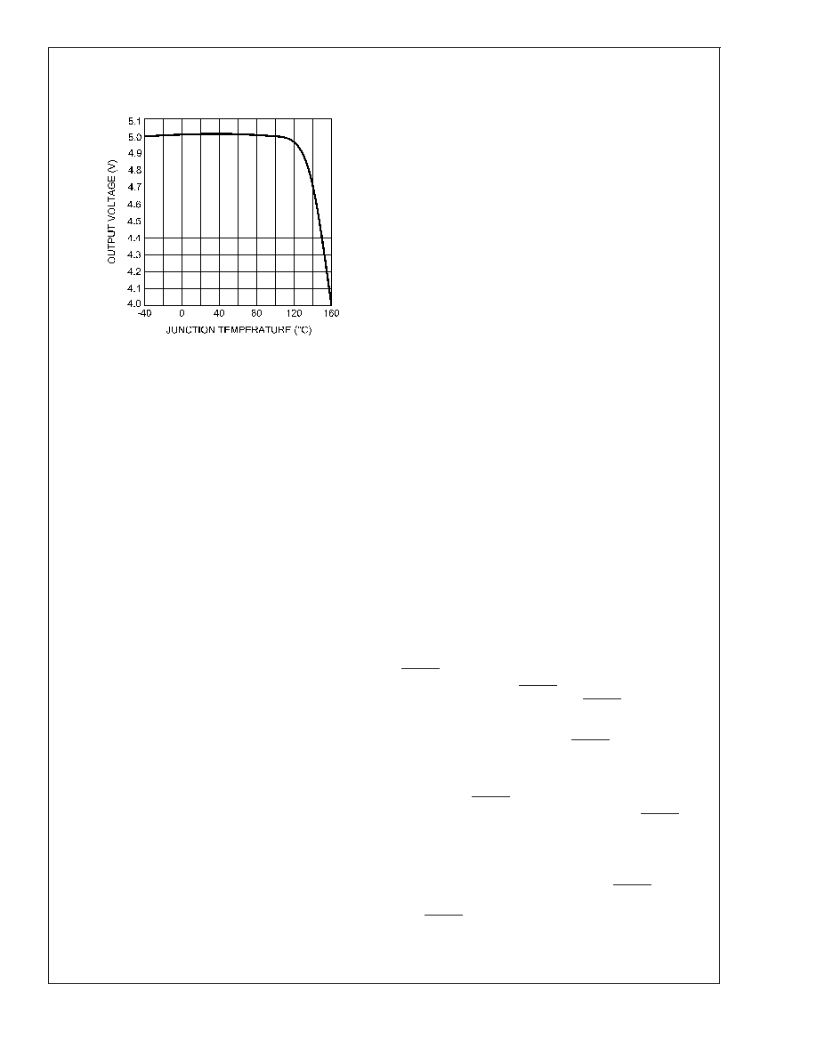
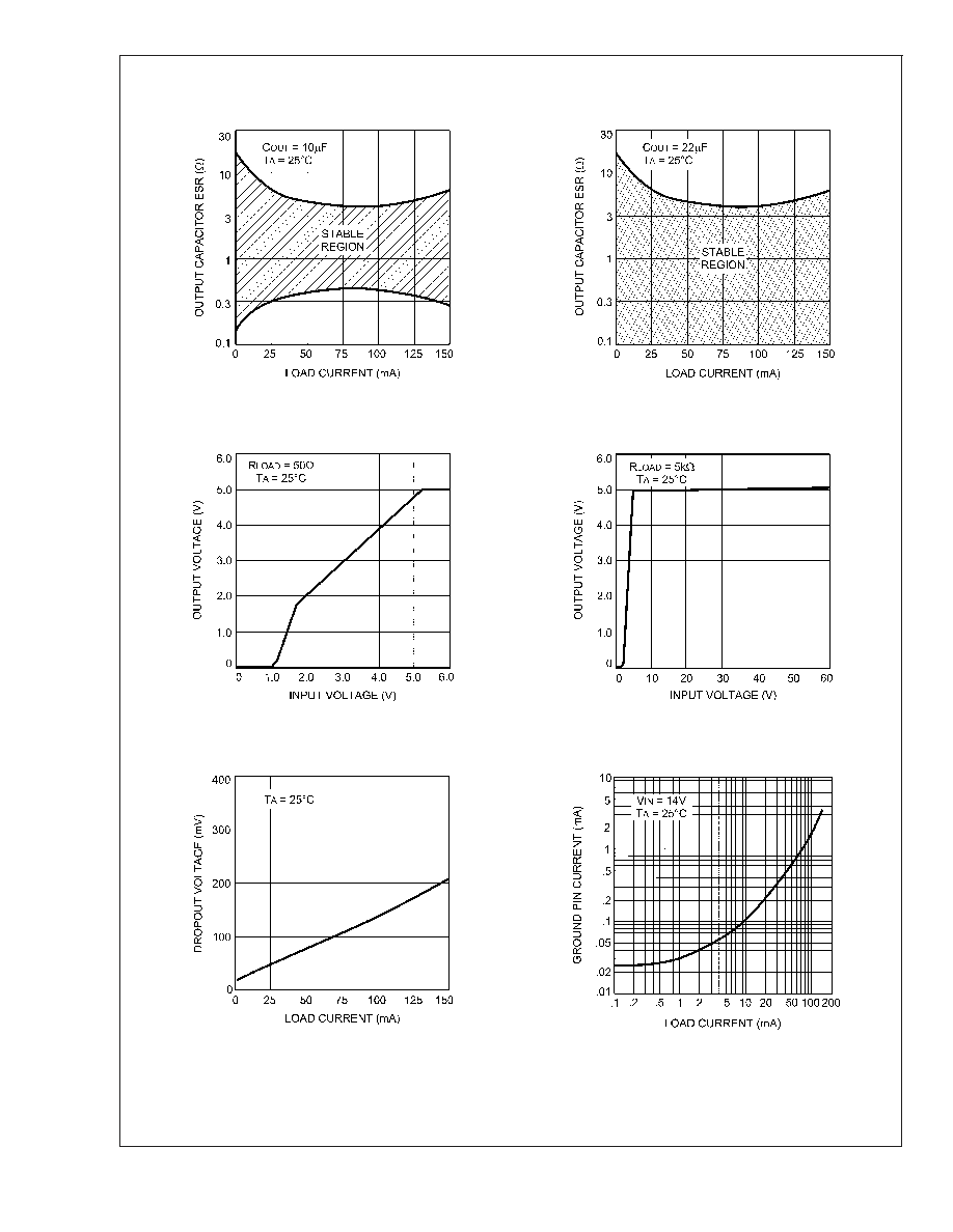
Typical Performance Characteristics
(Continued)
Output Voltage vs Junction Temperature
20083038
Application Information
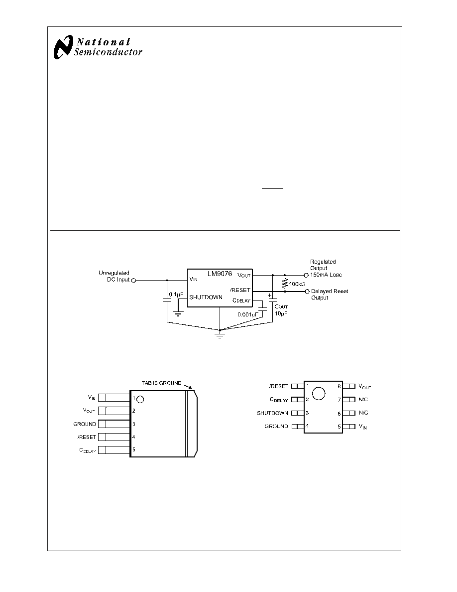
REGULATOR BASICS
This regulator is suitable for Automotive applications where
continuous connection to the battery is required (refer to the
Typical Application circuit).
The pass transistor of the regulator is an PNP device. A 10uF
capacitor on the V
OUT
pin will provide adequate performance
in most circumstances. There is no maximum value for the
regulator output bypass capacitance.
INPUT CAPACITOR
The LM9076 requires a low source impedance to maintain
regulator stability because portions of the internal bias cir-
cuitry are connected directly to V
IN
. At a minimum, at 0.1µF
ceramic capacitor should be placed between the LM9076
V
IN
and Ground pins, as close as is physically possible.
OUTPUT CAPACITOR
An output capacitor is also required for stability. This capaci-
tor must be placed between the LM9076 V
OUT
and Ground
pins, as close as is physically possible, using traces that are
not part of the main load current path.
The output capacitor must meet the requirements for mini-
mum capacitance and also maintain the appropriate ESR
value of the full operating ambient temperature range to
assure stability. There is no maximum limit for the output
capacitance value, as long as ESR is maintained. See the
Typical Performance Characteristics curves for details.
Solid tantalum capacitors are recommended as they gener-
ally maintain capacitance and ESR ratings over a wide tem-
perature range.
Ceramic capacitor types XR7 and X5R may be used if a
series resistor is added to simulate the ESR requirement.
Aluminum electrolytic capacitors are not recommend, as
they are subject to wide changes in capacitance and ESR
values across temperature.
DELAY CAPACITOR
The capacitor on the Delay pin must be a low leakage type
since the charge current is minimal (500nA typical) and the
pin must fully charge to 5V. Ceramic, Mylar, and polystyrene
capacitor types are generally recommended, although
changes in capacitance values across temperature changes
will have some effect on the delay timing.
SHUTDOWN PIN
The basic On/Off control of the regulator is accomplished
with the SHUTDOWN pin. By pulling the SHUTDOWN pin
high the regulator output is switched Off. When the regulator
is switched Off the load on the battery will be primarily due to
the SHUTDOWN pin current.
When the SHUTDOWN pin is low, or left open, the regulator
is switched On. When an unregulated supply, such as V
BATTERY , is used to pull the SHUTDOWN pin high a series
resistor in the range of 10K
to 50K is recommended to
provide reverse voltage transient protection of the SHUT-
DOWN pin. Adding a small capacitor (0.001uF typical) from
the SHUTDOWN pin to Ground will add noise immunity to
prevent accidental turn on due to noise on the supply line.
RESET FLAG
Proper operation of the RESET circuity is not guaranteed for
V
IN
voltages of less than 2.0V. The RESET pin will provide
information on the status of the regulator V
OUT
voltage level.
Any condition that causes the V
OUT
voltage to drop to typi-
cally 89% normal would cause the RESET pin to go low. This
will warn of a system Vcc supply that may cause abnormal
operation.
Of course, when the regulator is switched Off in normal
operation the RESET pin will be low.
If the regulator is On, and then switched off, the RESET flag
will go low when the V
OUT
voltage stored on the output
capacitor has decayed adequately.
Excessive thermal dissipation of the device such that the
Thermal Shutdown circuit is activated which then switches
the regulator output Off, would cause the RESET pin to go
low.
The RESET pin is an open collector output and requires an
external pull-up resistor to V
OUT
. The external pull-up resis-
tor should be in the range of 10K
to 200K.
LM9076
www.national.com
5