 | –≠–ª–µ–∫—Ç—Ä–æ–Ω–Ω—ã–π –∫–æ–º–ø–æ–Ω–µ–Ω—Ç: LM92CIM | –°–∫–∞—á–∞—Ç—å:  PDF PDF  ZIP ZIP |
LM92
±
0.33∞C Accurate, 12-Bit + Sign Temperature Sensor and
Thermal Window Comparator with Two-Wire Interface
General Description
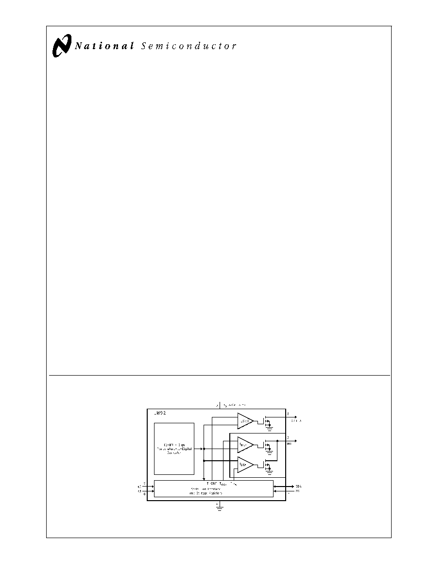
The LM92 is a digital temperature sensor and thermal win-
dow comparator with an I
2
C
TM
Serial Bus interface and an
accuracy of
±
0.33∞C. The window-comparator architecture
of the LM92 eases the design of temperature control sys-
tems. The open-drain Interrupt (INT) output becomes active
whenever temperature goes outside a programmable win-
dow,
while
a
separate
Critical
Temperature
Alarm
(T_CRIT_A) output becomes active when the temperature
exceeds a programmable critical limit. The INT output can
operate in either a comparator or event mode, while the
T_CRIT_A output operates in comparator mode only.
The host can program both the upper and lower limits of the
window as well as the critical temperature limit. Program-
mable hysterisis as well as a fault queue are available to
minimize false tripping. Two pins (A0, A1) are available for
address selection. The sensor powers up with default thresh-
olds of 2∞C T
HYST
, 10∞C T
LOW
, 64∞C T
HIGH
, and 80∞C
T_CRIT.
The LM92's 2.7V to 5.5V supply voltage range, Serial Bus in-
terface, 12-bit + sign output, and full-scale range of over
128∞C make it ideal for a wide range of applications. These
include thermal management and protection applications in
personal computers, electronic test equipment, office elec-
tronics, automotive, medical and HVAC applications.
Features
n
Window comparison simplifies design of ACPI
compatible temperature monitoring and control.
n
Serial Bus interface
n
Separate open-drain outputs for Interrupt and Critical
Temperature shutdown
n
Shutdown mode to minimize power consumption
n
Up to 4 LM92s can be connected to a single bus
n
12-bit + sign output
n
Operation up to 150∞C
Key Specifications
n
Supply Voltage
2.7V to 5.5V
n
Supply Current
operating
350µA (typ)
625µA (max)
shutdown
5µA (typ)
n
Temperature
30∞C
±
0.33∞C(max)
Accuracy
10∞C to 50∞C
±
0.50∞C(max)
-10∞C to 85∞C
±
1.0∞C(max)
125∞C
±
1.25∞C(max)
-25∞C to 150∞C
±
1.5∞C(max)
n
Linearity
±
0.5∞C(max)
n
Resolution
0.0625∞C
Applications
n
HVAC
n
Medical Electronics
n
Electronic Test Equipment
n
System Thermal Management
n
Personal Computers
n
Office Electronics
n
Automotive
Simplified Block Diagram
I2C
Æ
is a registered trademark of Philips Corporation.
DS101051-1
March 2000
LM92
±
0.33∞C
Accurate,
12-Bit
+
Sign
T
emperature
Sensor
and
Thermal
W
indow
Comparator
with
T
wo-W
ire
Interface
© 2000 National Semiconductor Corporation
DS101051
www.national.com
Connection Diagram
Ordering Information
Order Number
Supply Voltage
Supplied As
LM92CIM
2.7V to 5.5V
LM92CIMX
2.7V to 5.5V
2500 Units on Tape and Reel
Pin Descriptions
Label
Pin #
Function
Typical Connection
SDA
1
Serial Bi-Directional Data Line. Open Drain Output
From Controller
SCL
2
Serial Bus Clock Input
From Controller
T_CRIT_A
3
Critical Temperature Alarm Open Drain Output
Pull Up Resistor, Controller Interrupt Line
or System Hardware Shutdown
GND
4
Power Supply Ground
Ground
INT
5
Interrupt Open Drain Output
Pull Up Resistor, Controller Interrupt Line
+V
S
8
Positive Supply Voltage Input
DC Voltage from 2.7V to 5.5V
A0≠A1
7,6
User-Set Address Inputs
Ground (Low, "0") or +V
S
(High, "1")
Typical Application
SO-8
DS101051-2
LM92
See NS Package Number M08A
DS101051-3
LM92
www.national.com
2
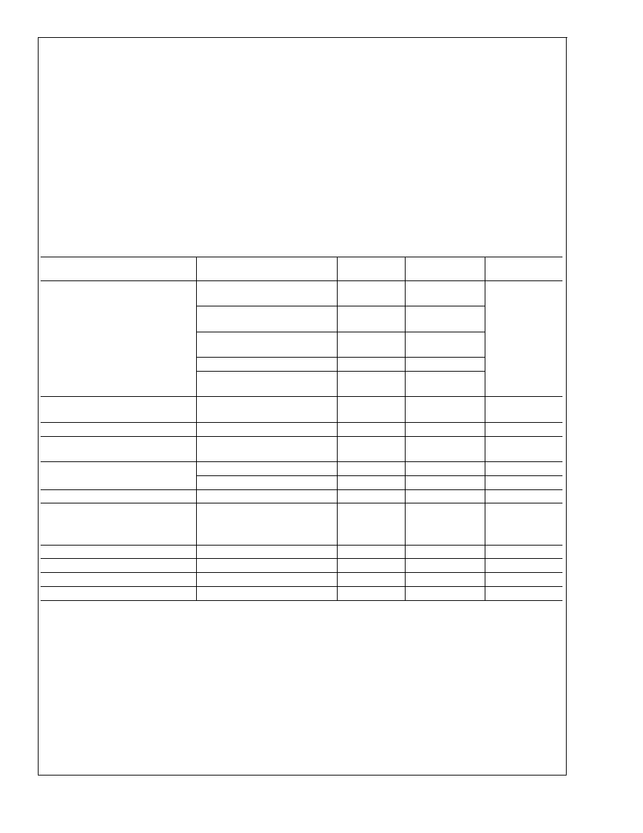
Absolute Maximum Ratings
(Note 1)
Supply Voltage
-0.3 V to 6.5V
Voltage at any Pin
-0.3 V
to (+V
S
+ 0.3V)
Input Current at any Pin
5mA
Package Input Current (Note 2)
20mA
T_CRIT_A and INT Output Sink
Current
10mA
T_CRIT_A and INT Output
Voltage
6.5V
Storage Temperature
-65∞C to +125∞C
Soldering Information, Lead
Temperature
SOP and MSOP Package (Note 3)
Vapor Phase (60 seconds)
215∞C
Infrared (15 seconds)
220∞C
ESD Susceptibility (Note 4)
Human Body Model
2500V
Machine Model
250V
Operating Ratings
(Notes 1, 5)
Specified Temperature Range
T
MIN
to T
MAX
(Note 6)
-55∞C to +150∞C
Supply Voltage Range (+V
S
)
+2.7V to +5.5V
Electrical Characteristics
Temperature-to-Digital Converter CharacteristicsUnless otherwise noted, these specifications apply for +V
S
=+2.7V to +5.5V
for LM92CIM . Boldface limits apply for T
A
= T
J
= T
MIN
to T
MAX
; all other limits T
A
= T
J
=+25∞C, unless otherwise noted.
Parameter
Conditions
Typical
(Note 7)
Limits
(Note 8)
Units
(Limit)
Accuracy (This is a summary. For
more detailed information please
see (Note 9))
T
A
= +30∞C, +V
S
= 3.3V to
4.0V
±
0.33
∞C (max)
T
A
= 10∞C or +50∞C, +V
S
=
3.3V to 4.0V
±
0.50
T
A
= -10 ∞C or +85∞C, +V
S
=
3.3V to 4.0V
±
1.00
T
A
= +125∞C, +V
S
= 4.0V
±
1.25
T
A
= -25∞C to 150∞C, +V
S
=
4.0V
±
1.50
Resolution
(Note 10)
13
0.0625
Bits
∞C
Linearity (Note 11)
±
0.5
∞C (max)
Offset Error of Transfer Function
(Note 12)
+V
S
= 4.0V
∞C (max)
Offset Error of Transfer Function
Supply Sensitivity
2.7V
+V
S
<
3.6V
∞C/V (max)
3.6V
+V
S
5.5V
∞C/V (max)
Temperature Conversion Time
(Note 13)
500
1000
ms
Quiescent Current
I
2
C Inactive
0.35
mA
I
2
C Active
0.35
0.625
mA (max)
Shutdown Mode
5
µA
T
HYST
Default Temperature
(Notes 15, 16)
2
∞C
T
LOW
Default Temperature
(Note 16)
10
∞C
T
HIGH
Default Temperature
(Note 16)
64
∞C
T
C
Default Temperature
(Note 16)
80
∞C
LM92
www.national.com
3
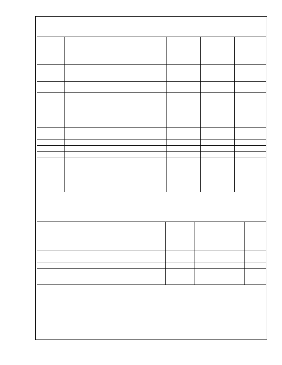
Electrical Characteristics
DIGITAL DC CHARACTERISTICSUnless otherwise noted, these specifications apply for +V
S
=+2.7V to +5.5V for LM92CIM .
Boldface limits apply for T
A
= T
J
= T
MIN
to T
MAX
; all other limits T
A
= T
J
=+25 ∞C, unless otherwise noted.
Symbol
Parameter
Conditions
Typical
(Note 7)
Limits
(Note 8)
Units
(Limit)
V
IN(1)
SDA and SCL Logical "1" Input
Voltage
+V
S
x 0.7
V (min)
+V
S
+0.3
V (max)
V
IN(0)
SDA and SCL Logical "0" Input
Voltage
-0.3
V (min)
+V
S
x 0.3
V (max)
V
IN(HYST)
SDA and SCL Digital Input
Hysteresis
500
250
mV (min)
V
IN(1)
A0 and A1 Logical "1" Input
Voltage
2.0
V (min)
+V
S
+0.3
V (max)
V
IN(0)
A0 and A1 Logical "0" Input
Voltage
-0.3
V (min)
0.7
V (max)
I
IN(1)
Logical "1" Input Current
V
IN
= + V
S
0.005
1.0
µA (max)
I
IN(0)
Logical "0" Input Current
V
IN
= 0 V
-0.005
-1.0
µA (max)
C
IN
Capacitance of All Digital Inputs
20
pF
I
OH
High Level Output Current
V
OH
= + V
S
10
µA (max)
V
OL
Low Level Output Voltage
I
OL
= 3 mA
0.4
V (max)
T_CRIT_A Output Saturation
Voltage
I
OUT
= 4.0 mA
(Note 14)
0.8
V (max)
T_CRIT_A Delay
1
Conversions
(max)
t
OF
Output Fall Time
C
L
= 400 pF
250
ns (max)
I
O
= 3 mA
SERIAL BUS DIGITAL SWITCHING CHARACTERISTICS Unless otherwise noted, these specifications apply for +V
S
=+2.7V
to +5.5V for LM92CIM . Boldface limits apply for T
A
= T
J
= T
MIN
to T
MAX
; all other limits T
A
= T
J
=+25 ∞C, unless otherwise
noted. CL (load capacitance) on output lines = 80 pF unless otherwise specified. Boldface limits apply for T
A
= T
J
= T
MIN
to
T
MAX
; all other limits T
A
= T
J
= +25 ∞C, unless otherwise noted.
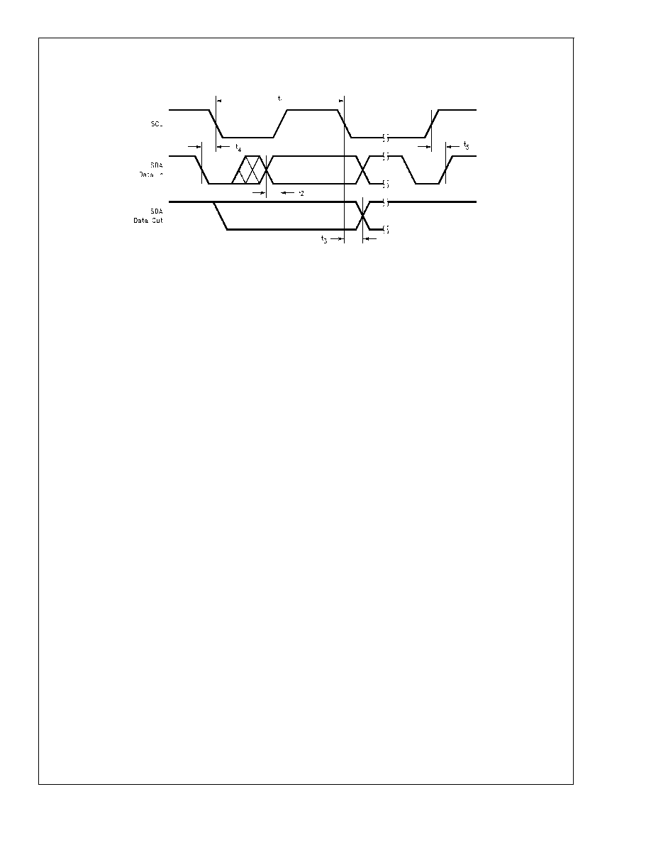
The switching characteristics of the LM92 fully meet or exceed the published specifications of the I
2
C bus. The following pa-
rameters are the timing relationship between SCL and SDA signal related to the LM92. They are not the I
2
C bus specifica-
tions.
Symbol
Parameter
Conditions
Typical
(Note 7)
Limits
(Note 8)
Units
(Limit)
t
1
SCL (Clock) Period
2.5
µs(min)
1
ms(max)
t
2
Data in Set-Up Time to SCL High
100
ns(min)
t
3
Data Out Stable after SCL Low
0
ns(min)
t
4
SDA Low Set-Up Time to SCL Low (Start Condition)
100
ns(min)
t
5
SDA High Hold Time after SCL High (Stop Condition)
100
ns(min)
t
TIMEOUT
SDA and SCL Time Low for Reset of Serial Interface
(Note 17)
75
300
ms (min)
ms
(max)
LM92
www.national.com
4
Electrical Characteristics
(Continued)
Note 1: Absolute Maximum Ratings indicate limits beyond which damage to the device may occur. DC and AC electrical specifications do not apply when operating
the device beyond its rated operating conditions.
Note 2: When the input voltage (V
I
) at any pin exceeds the power supplies (V
I
<
GND or V
I
>
+V
S
) the current at that pin should be limited to 5 mA. The 20 mA
maximum package input current rating limits the number of pins that can safely exceed the power supplies with an input current of 5 mA to four.
Note 3: See AN-450 "Surface Mounting Methods and Their Effect on Product Reliability" or the section titled "Surface Mount" found in a current National Semicon-
ductor Linear Data Book for other methods of soldering surface mount devices.
Note 4: Human body model, 100 pF discharged through a 1.5 k
resistor. Machine model, 200 pF discharged directly into each pin.
Note 5: LM92
JA
(thermal resistance, junction-to-ambient) when attached to a printed circuit board with 2 oz. foil is 200 ∞C/W.
Note 6: While the LM92 has a full-scale-range in excess of 128 ∞C, prolonged operation at temperatures above 125 ∞C is not recommended.
Note 7: Typicals are at T
A
= 25 ∞C and represent most likely parametric norm.
Note 8: Limits are guaranteed to National's AOQL (Average Outgoing Quality Level).
Serial Bus Communication
DS101051-4
LM92
www.national.com
5