Äîêóìåíòàöèÿ è îïèñàíèÿ www.docs.chipfind.ru
LM94021
Multi-Gain Analog Temperature Sensor
General Description
The
LM94021
is
a
precision
analog
output
CMOS
integrated-circuit temperature sensor that operates at a sup-
ply voltage as low as 1.5V. While operating over the wide
temperature range of -50°C to +150°C, the LM94021 deliv-
ers an output voltage that is inversely porportional to mea-
sured temperature. The LM94021's low supply current
makes it ideal for battery-powered systems as well as gen-
eral temperature sensing applications.
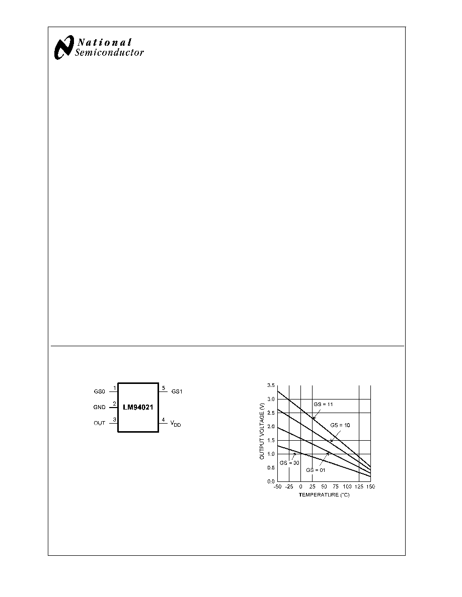
Two logic inputs, Gain Select 1 (GS1) and Gain Select 0
(GS0), select the gain of the temperature-to-voltage output
transfer function. Four slopes are selectable: -5.5 mV/°C,
-8.2 mV/°C, -10.9 mV/°C, and -13.6 mV/°C. In the lowest
gain configuration (GS1 and GS0 both tied low), the
LM94021 can operate with a 1.5V supply while measuring
temperature over the full -50°C to +150°C operating range.
Tying both inputs high causes the transfer function to have
the largest gain of -13.6 mV/°C for maximum temperature
sensitivity. The gain-select inputs can be tied directly to V
DD
or Ground without any pull-up or pull-down resistors, reduc-
ing component count and board area. These inputs can also
be driven by logic signals allowing the system to optimize the
gain during operation or system diagnostics.
Applications
n
Cell phones
n
Wireless Transceivers
n
Battery Management
n
Automotive
n
Disk Drives
n
Games
n
Appliances
Features
n
Low 1.5V operation
n
Four selectable gains
n
Very accurate over wide temperature range of -50°C to
+150°C
n
Low quiescent current
n
Output is short-circuit protected
n
Extremely small SC70 package
n
Footprint compatible with the industry-standard LM20
temperature sensor
Key Specifications
j
Supply Voltage
1.5V to 5.5V
j
Supply Current
9 µA (typ)
j
Temperature
Accuracy
20°C to 40°C
-50°C to 70°C
-50°C to 90°C
-50°C to 150°C
±
1.5°C
±
1.8°C
±
2.1°C
±
2.7°C
j
Operating
Temperature
-50°C to 150°C
Connection Diagram
SC70-5
20108601
Top View
See NS Package Number MAA05A
Typical Transfer Characteristic
Output Voltage vs Temperature
20108624
February 2005
LM94021
Multi-Gain
Analog
T
emperature
Sensor
© 2005 National Semiconductor Corporation
DS201086
www.national.com
Typical Application
Full-Range Celsius Temperature Sensor (-50°C to +150°C)
Operating from a Single Battery Cell
20108602
Ordering Information
Order
Temperature
NS Package
Device
Number
Accuracy
Number
Marking
Transport Media
LM94021BIMG
±
1.5°C to
±
2.7°C
MAA05A
21B
3000 Units on Tape and Reel
LM94021BIMGX
±
1.5°C to
±
2.7°C
MAA05A
21B
9000 Units on Tape and Reel
Pin Descriptions
Label
Pin
Number
Type
Equivalent Circuit
Function
GS1
5
Logic
Input
Gain Select 1 - One of two inputs for selecting
the slope of the output response
GS0
1
Logic
Input
Gain Select 0 - One of two inputs for selecting
the slope of the output response
OUT
3
Analog
Output
Outputs a voltage which is inversely
proportional to temperature
V
DD
4
Power
Positive Supply Voltage
GND
2
Ground
Power Supply Ground
LM94021
www.national.com
2
Absolute Maximum Ratings
(Note 1)
Supply Voltage
-0.2V to +6.0V
Voltage at Output Pin
-0.2V to (V
DD
+ 0.5V)
Output Current
±
7 mA
Voltage at GS0 and GS1 Input
Pins
-0.2V to +6.0V
Input Current at any pin (Note 2)
5 mA
Storage Temperature
-65°C to +150°C
Maximum Junction Temperature
(T
JMAX
)
+150°C
ESD Susceptibility (Note 3) :
Human Body Model
2500V
Machine Model
250V
Soldering process must comply with National's
Reflow Temperature Profile specifications. Refer to
www.national.com/packaging. (Note 4)
Operating Ratings
(Note 1)
Specified Temperature Range:
T
MIN
T
A
T
MAX
LM94021
-50°C
T
A
+150°C
Supply Voltage Range (V
DD
)
+1.5 V to +5.5 V
Thermal Resistance (
JA
) (Note 5)
SC-70
415°C/W
Accuracy Characteristics
These limits do not include DC load regulation. These stated accuracy limits are with reference to the values in the LM94021
Transfer Table.
Parameter
Conditions
Limits
(Note
7)
Units
(Limit)
Temperature
Error
(Note 8)
GS1=0
GS0=0
T
A
= +20°C to +40°C; V
DD
= 1.5V to 5.5V
±
1.5
°C (max)
T
A
= +0°C to +70°C; V
DD
= 1.5V to 5.5V
±
1.8
°C (max)
T
A
= +0°C to +90°C; V
DD
= 1.5V to 5.5V
±
2.1
°C (max)
T
A
= +0°C to +120°C; V
DD
= 1.5V to 5.5V
±
2.4
°C (max)
T
A
= +0°C to +150°C; V
DD
= 1.5V to 5.5V
±
2.7
°C (max)
T
A
= -50°C to +0°C; V
DD
= 1.6V to 5.5V
±
1.8
°C (max)
GS1=0
GS0=1
T
A
= +20°C to +40°C; V
DD
= 1.8V to 5.5V
±
1.5
°C (max)
T
A
= +0°C to +70°C; V
DD
= 1.9V to 5.5V
±
1.8
°C (max)
T
A
= +0°C to +90°C; V
DD
= 1.9V to 5.5V
±
2.1
°C (max)
T
A
= +0°C to +120°C; V
DD
= 1.9V to 5.5V
±
2.4
°C (max)
T
A
= +0°C to +150°C; V
DD
= 1.9V to 5.5V
±
2.7
°C (max)
T
A
= -50°C to +0°C; V
DD
= 2.3V to 5.5V
±
1.8
°C (max)
GS1=1
GS0=0
T
A
= +20°C to +40°C; V
DD
= 2.2V to 5.5V
±
1.5
°C (max)
T
A
= +0°C to +70°C; V
DD
= 2.4V to 5.5V
±
1.8
°C (max)
T
A
= +0°C to +90°C; V
DD
= 2.4V to 5.5V
±
2.1
°C (max)
T
A
= +0°C to +120°C; V
DD
= 2.4V to 5.5V
±
2.4
°C (max)
T
A
= +0°C to +150°C; V
DD
= 2.4V to 5.5V
±
2.7
°C (max)
T
A
= -50°C to +0°C; V
DD
= 3.0V to 5.5V
±
1.8
°C (max)
GS1=1
GS0=1
T
A
= +20°C to +40°C; V
DD
= 2.7V to 5.5V
±
1.5
°C (max)
T
A
= +0°C to +70°C; V
DD
= 3.0V to 5.5V
±
1.8
°C (max)
T
A
= +0°C to +90°C; V
DD
= 3.0V to 5.5V
±
2.1
°C (max)
T
A
= +0°C to +120°C; V
DD
= 3.0V to 5.5V
±
2.4
°C (max)
T
A
= 0°C to +150°C; V
DD
= 3.0V to 5.5V
±
2.7
°C (max)
T
A
= -50°C to +0°C; V
DD
= 3.6V to 5.5V
±
1.8
°C (max)
LM94021
www.national.com
3
Electrical Characteristics
Unless otherwise noted, these specifications apply for +V
DD
= +1.5V to +5.5V . Boldface limits apply for T
A
= T
J
= T
MIN
to
T
MAX
; all other limits T
A
= T
J
= 25°C.
Symbol
Parameter
Conditions
Typical
(Note 6)
Limits (Note 7)
Units
(Limit)
Sensor Gain
GS1 = 0, GS0 = 0
GS1 = 0, GS1 = 1
GS1 = 1, GS0 = 0
GS1 = 1, GS0 = 1
-5.5
-8.2
-10.9
-13.6
mV/°C
mV/°C
mV/°C
mV/°C
Load Regulation
(Note 10)
Source
2.0 µA (Note 11)
Sink
100 µA
Sink = 50 µA
0.4
-1
1.6
mV (max)
mV (max)
mV
Line Regulation (Note
14)
(V
DD
- V
OUT
)
200 mV
200
µV/V
I
S
Supply Current
T
A
= +30°C to +150°C
T
A
= -50°C to +150°C
9
12
13
µA (max)
µA (max)
C
L
Output Load
Capacitance
1100
pF (max)
Power-on Time
(Note 12)
C
L
= 0 pF
C
L
=1100 pF
0.7
0.8
5
10
ms (max)
ms (max)
V
IH
GS1 and GS0 Input
Logic "1" Threshold
Voltage
V
DD
- 0.5V
V (min)
V
IL
GS1 and GS0 Input
Logic "0" Threshold
Voltage
0.5
V (max)
I
IH
Logic "1" Input Current
(Note 13)
0.001
1
µA (max)
I
IL
Logic "0" Input Current
(Note 13)
0.001
1
µA (max)
Note 1: Absolute Maximum Ratings indicate limits beyond which damage to the device may occur. Operating Ratings indicate conditions for which the device is
functional, but do not guarantee specific performance limits. For guaranteed specifications and test conditions, see the Electrical Characteristics. The guaranteed
specifications apply only for the test conditions listed. Some performance characteristics may degrade when the device is not operated under the listed test
conditions.
Note 2: When the input voltage (V
I
) at any pin exceeds power supplies (V
I
<
GND or V
I
>
V
+
), the current at that pin should be limited to 5 mA.
Note 3: The human body model is a 100 pF capacitor discharged through a 1.5 k
resistor into each pin. The machine model is a 200 pF capacitor discharged
directly into each pin.
Note 4: Reflow temperature profiles are different for lead-free and non-lead-free packages.
Note 5: The junction to ambient thermal resistance (
JA
) is specified without a heat sink in still air.
Note 6: Typicals are at T
J
= T
A
= 25°C and represent most likely parametric norm.
Note 7: Limits are guaranteed to National's AOQL (Average Outgoing Quality Level).
Note 8: Accuracy is defined as the error between the measured and reference output voltages, tabulated in the Transfer Table at the specified conditions of supply
gain setting, voltage, and temperature (expressed in °C). Accuracy limits include line regulation within the specified conditions. Accuracy limits do not include load
regulation; they assume no DC load.
Note 9: Changes in output due to self heating can be computed by multiplying the internal dissipation by the thermal resistance.
Note 10: Source currents are flowing out of the LM94021. Sink currents are flowing into the LM94021.
Note 11: Assumes (V
DD
- V
OUT
) ^ 200mV.
Note 12: Guaranteed by design.
Note 13: The input current is leakage only and is highest at high temperature. It is typically only 0.001µA. The 1µA limit is solely based on a testing limitation and
does not reflect the actual performance of the part.
Note 14: Line regulation is calculated by subtracting the output voltage at the highest supply voltage from the output voltage at the lowest supply voltage. The typical
line regulation specification does not include the output voltage shift discussed in Section 5.0.
LM94021
www.national.com
4
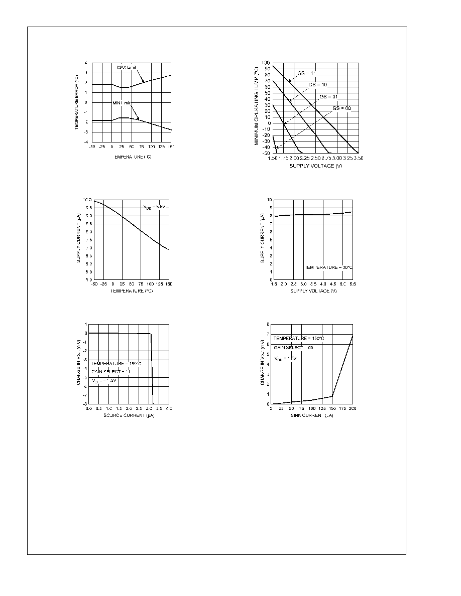
Typical Performance Characteristics
Temperature Error vs. Temperature
Minimum Operating Temperature vs. Supply Voltage
20108607
20108606
Supply Current vs. Temperature
Supply Current vs. Supply Voltage
20108604
20108605
Load Regulation, Sourcing Current
Load Regulation, Sinking Current
20108640
20108641
LM94021
www.national.com
5
Document Outline