 | –≠–ª–µ–∫—Ç—Ä–æ–Ω–Ω—ã–π –∫–æ–º–ø–æ–Ω–µ–Ω—Ç: LM9617 | –°–∫–∞—á–∞—Ç—å:  PDF PDF  ZIP ZIP |
©
2000 National Semiconductor Corporation
Confidential
www.national.com
March 2001
LM9617
Monochrome
CMOS Image Sensor VGA 30 FPS
General Description
The LM9617 is a high performance, low power, third inch VGA
CMOS Active Pixel Sensor capable of capturing grey-scale digi-
tal still or motion images and converting them to a digital data
stream.
In addition to the active pixel array, an on-chip 12 bit A/D conver-
tor, fixed pattern noise elimination circuits and a video gain is
provided. Furthermore, an integrated programmable smart tim-
ing and control circuit allows the user maximum flexibility in
adjusting integration time, active window size, gain and frame
rate. Various control, timing and power modes are also provided.
Features
∑ Supplied with micro lenses
∑ Video or snapshot operations
∑ Progressive scan and interlace read out modes.
∑ Programmable pixel clock, inter-frame and inter-line delays.
∑ Programmable partial or full frame integration
∑ Programmable gain
∑ Horizontal & vertical sub-sampling (2:1 & 4:2)
∑ Windowing
∑ External snapshot trigger & event synchronisation signals
∑ Auto black level compensation
∑ Flexible digital video read-out supporting programmable:
- polarity for synchronisation and pixel clock signals
- leading edge adjustment for horizontal synchronization
∑ Programmable via 2 wire I
2
C compatible serial interface
∑ Power on reset & power down mode
Applications
∑ Security Cameras
∑ Toys
∑ Machine Vision
∑ Biometrics
∑ Infrared Camera
∑ Barcode Scanner
Key Specifications
∑ Array Format
Total: 664H x 504V
Active: 648H x 488V
∑ Effective Image Area
Total: 4.98mm x 3.78 mm
Active: 4.86 mm x 3.66 mm
∑ Optical Format
1/3"
∑ Pixel Size
7.5
µ
m x 7.5
µ
m
∑ Video Outputs
8,10 & 12 Bit Digital
∑ Dynamic Range
57dB
∑ FPN
0.35%
Sensitivity
28.7 Kilo LSBs / lux.s
∑ Quantum Efficiency
27%
∑ Fill Factor
47% (no micro lens)
∑ Package
48 LCC
∑ Single Supply
3.3 V
∑ Power Consumption
90 mW
∑ Operating Temp
0 to 50
o
C
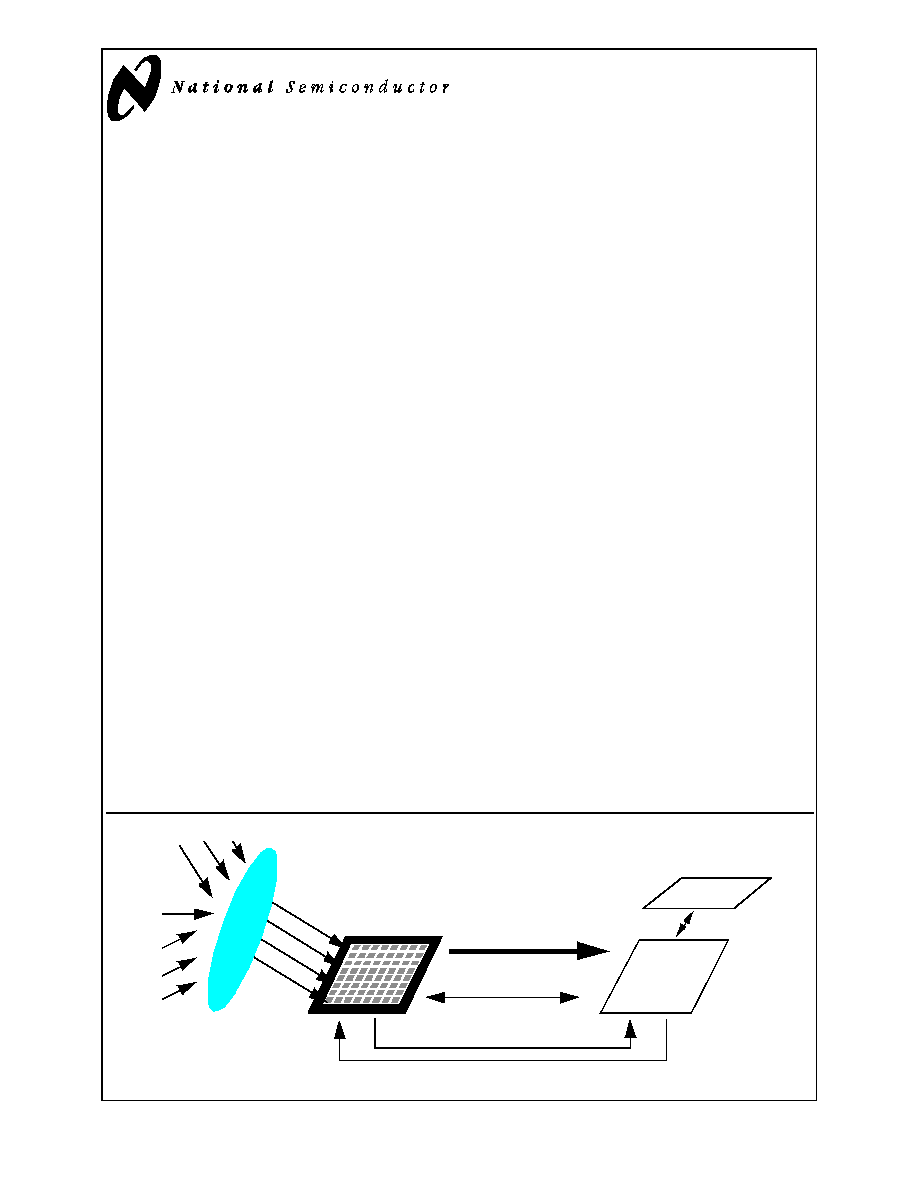
12bit digital image
lens
I
2
C compatible
Digital Image
Processor
Storage
snapshot
event trigger
LM9617
System Block Diagram
L
M
9
6
1
7
M
o
n
o
c
h
r
o
m
e
C
M
O
S
I
m
a
g
e
S
e
n
s
o
r
V
G
A
3
0
F
P
S
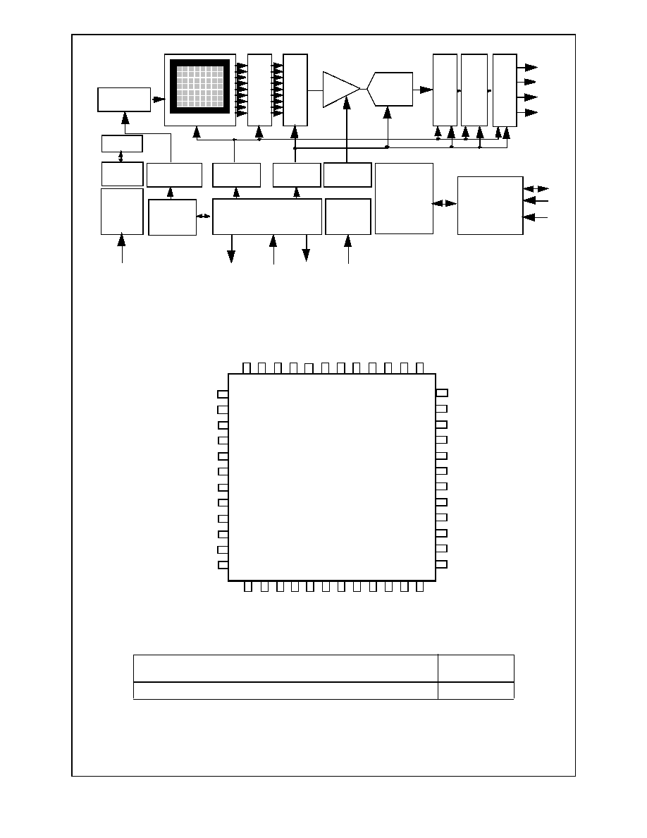
Confidential
2
www.national.com
C
o
l
u
m
n
C
D
S
APS Array
H
o
r
i
z
o
n
t
a
l
S
h
i
f
t
R
e
g
i
s
t
e
r
POR
1
2 Bit A/D
AMP
B
a
d
P
i
x
e
l
D
e
t
e
c
t
&
C
o
r
r
e
c
t
D
i
g
i
t
a
l
V
i
d
e
o
F
r
a
m
e
r
B
l
a
c
k
L
e
v
e
l
C
o
m
p
e
n
s
a
t
i
o
n
d[11:0]
pclk
hsync
vsync
Row Address
Decoder
Vertical
Horizontal
Master Timer
Timing
Timing
Row Address
Gen
Clock Gen
I
2
C Compatible
Register Bank
Reset
Gen
Gain
Control
Serial I/F
sda
sclk
sadr
Power
Control
pdwn
snapshot
extsync
Controller
(sequencer)
irq
mclk
Overall Chip Block Diagram
Figure 1. Chip Block Diagram
7
9
10
11
12
13
14
15
16
18
17
42
40
39
38
37
36
35
34
33
31
32
sclk
resetb
pdwn
vss_dig
vdd_dig
vsync
pclk
mclk
d
1
d0
fine_i
v
s
s
_
o
d
1
v
s
s
_
o
d
3
gnd
fine_ctrl
offset
vdd_ana1
vdd_ana2
vss_ana2
s
d
a
s
a
d
r
i
r
q
v
d
d
_
p
i
x
v
r
l
v
s
r
v
d
d
e
x
t
s
y
n
c
v
d
d
_
o
d
1
6 5 4
3 2
1 48 47 46 45
NC
d
4
d
5
d
6
d
8
d
7
d
9
vdd_od2
vss_od2
19 20 21
23
22
24 25 26 27 28
30
48 PIN LCC
43
d
1
1
d
1
0
8
snapshot
41
N
C
44
vref_adc
29
d
3
d
2
LM9617
hsync
vss_ana1
v
d
d
_
o
d
3
NC
N
C
Connection Diagram
Ordering Information
Temperature
(0∞C
T
A
+
50∞C)
NS Package
LM9617 CCEA
LCC
L
M
9
6
1
7
Confidential
3
www.national.com
Typical Application Circuit
0.1
µ
F
1.5k
820
3.3V analog
0.1
µ
F
3.3V digital
12
9
37
36
35
7
6
8
10
vss_dig
r
e
s
e
t
b
vdd_ana1
vss_ana1
vref_adc
vdd_od1
vss_od1
s
a
d
r
e
x
t
s
y
n
c
s
c
l
k
s
d
a
d
9
d
8
d
7
d
5
d
6
d
4
d
1
d
0
s
n
a
p
s
h
o
t
30 29 28
26
27
25 24 23 22 21
17
d
2
d
3
11
vdd_dig
48
5
20
d
1
0
d
1
1
0.1
µ
F
3.3V analog
31
32
vdd_od2
vss_od2
0.1
µ
F
3.3V digital
0.1
µ
F
3.3V digital
47
46
vdd_pix
vrl
0.1
µ
F
3
2
1
vsrvdd
1.0
µ
F
13 14 15
h
s
y
n
c
v
s
y
n
c
p
c
l
k
LM9617
p
d
w
n
Serial Control Bus
System Control
Digital Video Bus
Camera Control
i
r
q
4
33
34
vdd_ana2
vss_ana2
0.1
µ
F
3.3V analog
16
m
c
l
k
vdd_od3
vss_od3
0.1
µ
F
44
45
fine_i 41
gnd 40
3.3V analog
3.3V digital
offset
fine_ctrl 39
NC
18
NC
19
NC
42
NC
43
1 0 k
1.2k
470
2N3904
1N4148
4.7
µ
F
vdd_ana
2 2 k
vdd_ana
38
1%
1%
1%
1%
Figure 2. Typical Application Diagram
Scan Read Out Direction
Figure 3. Scan directions and position of origin in imaging system
(0,0)
pin 1
CMOS Image Sensor
(0,0)
digital
out
lens
(0,0)
horizontal scan
v
e
r
t
i
c
a
l
s
c
a
n
L
M
9
6
1
7

Confidential
4
www.national.com
Pin Descriptions
Pin
Name
I/O
Typ
Description
1
vsrvdd
I0
P
Analog bidirectional, it should be connect to ground via a 1.0
µ
f capacitor. This pin is the
internal charge pump voltage source.
2
vrl
I
A
Anti blooming pin. This pin is normally tied to ground.
3
vdd_pix
I
P
3.3 volt supply for the pixel array.
4
irq
O
D
Digital output, the interrupt request pin. This pin generates interrupts during snapshot
mode.
5
sadr
I
D
Digital input with pull down resistor. This pin is used to program different slave addresses
for the sensor in an I
2
C compatible system.
6
sda
IO
D
I
2
C compatible serial interface data bus. The output stage of this pin has an open drain
driver.
7
sclk
I
D
I
2
C compatible serial interface clock.
8
snapshot
I
D
Digital input with pull down resistor used to activate (trigger) a snapshot sequence.
9
resetb
I
D
Digital input with pull up resistor. When forced to a logic 0 the sensor is reset to its default
power up state. The resetb signal is internally synchronized to mclk which must be run-
ning for a reset to occur.
10
pdwn
I
D
Digital input with pull down resistor. When forced to a logic 1 the sensor is put into power
down mode.
11
vss_dig
I
P
0 volt power supply for the digital circuits.
12
vdd_dig
I
P
3.3 volt power supply for the digital circuits.
13
hsync
IO
D
Digital Bidirectional. This is a dual mode pin. When the sensor's digital video port is con-
figured to be a master, (the default), this pin is an output and is the horizontal synchroni-
zation pulse. When the sensor's digital video port is configured to be a slave, this pin is
an input and is the row trigger.
14
vsync
IO
D
Digital Bidirectional. This is a dual mode pin. When the sensor's digital video port is con-
figured to be a master, (the default), this pin is an output and is the vertical synchroniza-
tion pulse. When the sensor's digital video port is configured to be a slave, this pin is an
input and is the frame trigger.
15
pclk
O
D
Digital output. The pixel clock.
16
mclk
I
D
Digital input. The sensor's master clock input.
17
d0
O
D
Digital output. Bit 0 of the digital video output bus. This output can be put into tri-state
mode.
18
NC
Pin not used, do not connect.
19
NC
Pin not used, do not connect.
20
d1
O
D
Digital output. Bit 1 of the digital video output bus. This output can be put into tri-state
mode.
21
d2
O
D
Digital output. Bit 2 of the digital video output bus. This output can be put into tri-state
mode.
22
d3
O
D
Digital output. Bit 3 of the digital video output bus. This output can be put into tri-state
mode.
23
d4
O
D
Digital output. Bit 4 of the digital video output bus. This output can be put into tri-state
mode.
24
d5
O
D
Digital output. Bit 5 of the digital video output bus. This output can be put into tri-state
mode.
25
d6
O
D
Digital output. Bit 6 of the digital video output bus. This output can be put into tri-state
mode.
L
M
9
6
1
7
Confidential
5
www.national.com
Pin Descriptions
(Continued)
Legend: (I=Input), (O=Output), (IO=Bi-directional), (P=Power), (D=Digital), (A=Analog).
Figure 4. Equivalent Circuits For
adc_ref and offset pins
Pin
Name
I/O
Typ
Description
26
d7
O
D
Digital output. Bit 7 of the digital video output bus. This output can be put into tri-state
mode.
27
d8
O
D
Digital output. Bit 8 of the digital video output bus. This output can be put into tri-state
mode.
28
d9
O
D
Digital output. Bit 9 of the digital video output bus. This output can be put into tri-state
mode.
29
d10
O
D
Digital output. Bit 10 of the digital video output bus. This output can be put into tri-state
mode.
30
d11
O
D
Digital output. Bit 11 of the digital video output bus. This output can be put into tri-state
mode.
31
vdd_od2
I
P
3.3 volt supply for the digital IO buffers.
32
vss_od2
I
P
0 volt supply for the digital IO buffers
33
vdd_ana2
I
P
3.3 volt supply for analog circuits.
34
vss_ana2
I
P
0 volt supply for analog circuits.
35
vref_adc
I
A
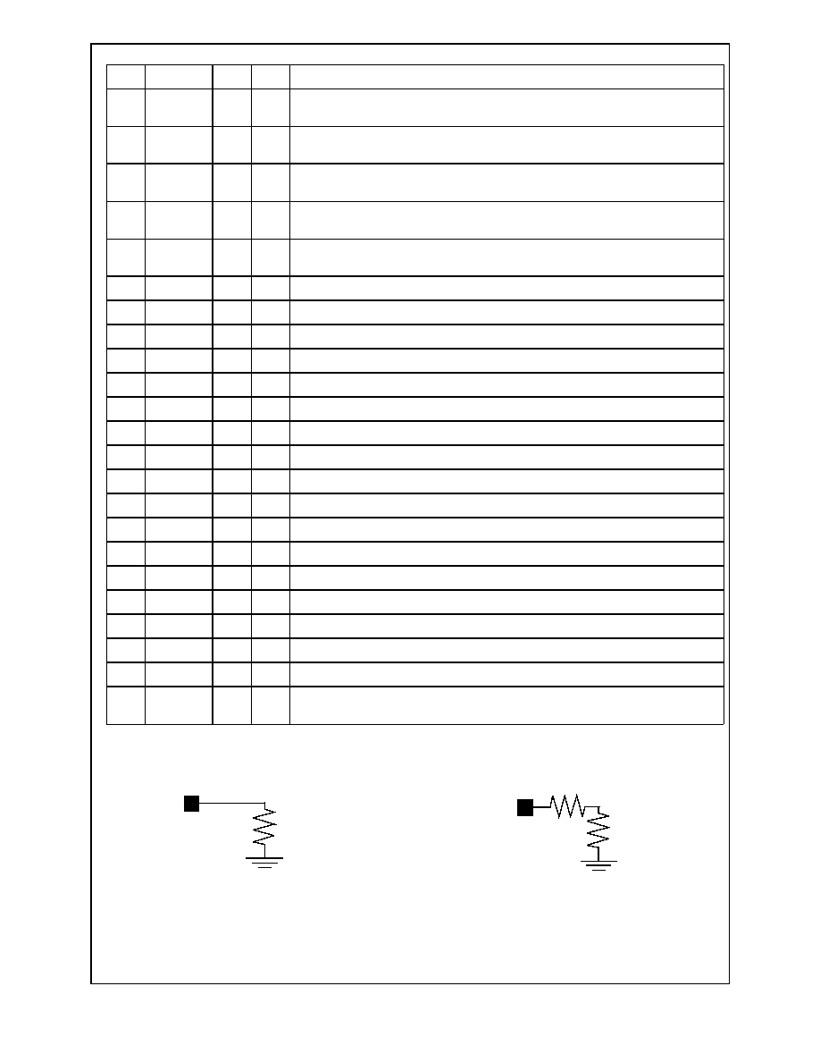
A/D reference resistor ladder voltage. See figure 4 for equivalent circuit.
36
vss_ana1
I
P
0 volt supply for analog circuits.
37
vdd_ana1
I
P
3.3 volt supply for analog circuits.
38
offset
I
A
Analog input used to adjust the offset of the sensor. See figure 4 for equivalent circuit.
39
fine_ctrl
O
A
Analog output used to drive the offset pin.
40
gnd
This pin must be tied to ground.
41
fine_i
I
A
Bias current for the fine offset adjust.
42
NC
Pin not used, do not connect.
43
NC
Pin not used, do not connect.
44
vdd_od3
I
P
3.3 volt supply for the sensor.
45
vss_od3
I
P
0 volt supply for the sensor.
46
vss_od1
I
P
0 volt supply for the digital IO buffers
47
vdd_od1
I
P
3.3 volt supply for the digital IO buffers.
48
extsync
O
D
Digital output. The external event synchronization signal is used to synchronize external
events in snapshot mode.
800
adc_vref
1K
200
offset
L
M
9
6
1
7