1
www.national.com
General Description
The LM9822 is a high performance Analog Front End (AFE) for
image sensor processing systems. It performs all the analog and
mixed signal functions (correlated double sampling, color spe-
cific gain and offset correction, and analog to digital conversion)
necessary to digitize the output of a wide variety of CIS and
CCD sensors. The LM9822 has a 14 bit 6MHz ADC.
Features
∑
6 million pixels/s conversion rate
∑
Digitally programmed gain and offset for red, green and blue
color balancing
∑
Correlated Double Sampling for lowest noise from CCD
sensors
∑
Compatible with CCD and CIS type image sensors
∑
Internal Voltage Reference Generation
∑
TTL/CMOS compatible input/output
Key Specifications
∑
Output Data Resolution
14 Bits
∑
Pixel Conversion Rate
6MHz
∑
Analog Supply Voltage
5V±5%
∑
I/O Supply Voltage
3.3V±10% or 5V±5%
∑
Power Dissipation (typical)
375mW
Applications
∑
Color Flatbed Document Scanners
∑
Color Sheetfed Scanners
∑
Multifunction Imaging Products
∑
Digital Copiers
∑
General Purpose Linear Array Imaging
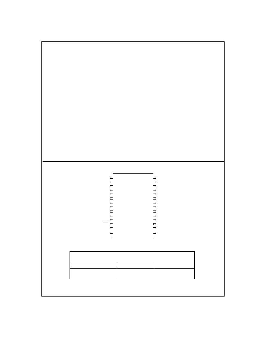
LM9822 3 Channel 42-Bit Color Scanner Analog Front End
Connection Diagram
LM9822
28 pin
SOIC
SCLK
SDI
SEN
D2
D0
V
D
DGND
D4
11
12
13
14
15
16
17
18
19
20
1
2
3
4
5
6
7
8
9
10
23
22
21
24
25
26
27
28
D7
D6
D5
MCLK
V
A
V
A
V
REF-
OS
B
OS
G
CLMP
OS
R
V
REF+
AGND
AGND
VSMP
SDO
V
REFMID
V
BANDGAP
D3
D1
May 1999
LM
98
22
3
C
h
a
n
n
e
l
42
-B
it
C
o
lo
r
S
c
an
ne
r
A
n
a
l
o
g
F
r
on
t
E
n
d
N
©1999 National Semiconductor Corporation
TRI-STATEÆ is a registered trademark of National Semiconductor Corporation.
Ordering Information
Notes:
1
- Rail transport media, 26 parts per rail,
2
- Tape and reel transport media, 1000 parts per reel
Temperature Range
0∞C
T
A
+70∞C
NS Package
Number
Order Number
Device Marking
LM9822CCWM
1
LM9822CCWMX
2
LM9822CCWM
LM9822CCWM
M28B
M28B
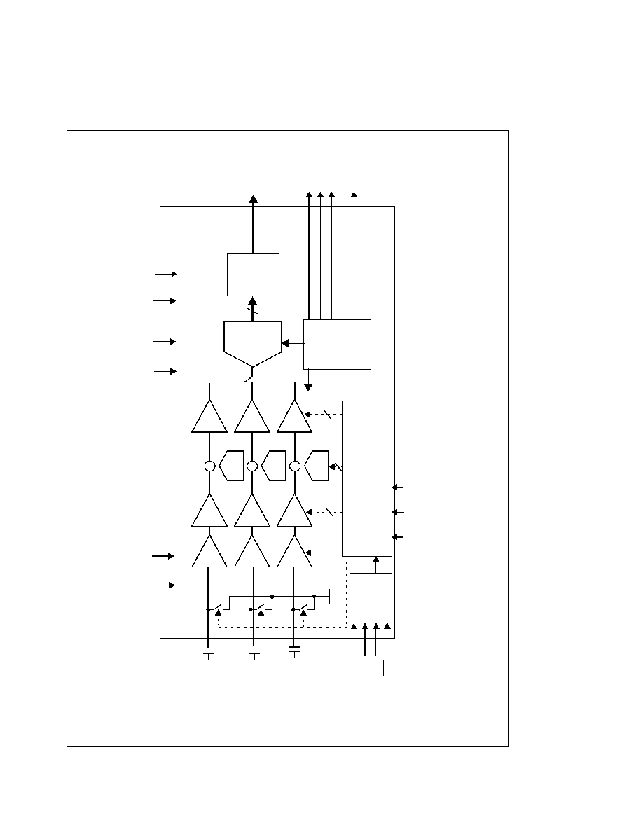
LM9822 Block Diagram
Serial
Interface
Coarse Color
Balance PGAs
DAC
R
Offset
+
+
OS
R
RED OS
from CCD
CDS
OS
G
GREEN OS
from CCD
CDS
OS
B
BLUE OS
from CCD
CDS
x0.93
to x3
DAC
G
Offset
+
+
DAC
B
Offset
+
+
VClamp
x1or x3
Static
Offset
DACs
V
BANDGAP
V
REF+
V
REFMID
V
REF-
Internal
Bandgap
Reference
x1or x3
x1or x3
Gain
Boost
x0.93
to x3
x0.93
to x3
Timing and Control
14
5
6
1
SCLK
SDI
SEN
V
A
V
D
AGND
DGND
V
A
AGND
MCLK
14 bits
to 8 bit
Bytes
D7 - D0
CLMP VSMP
14-Bit
ADC
SDO
2
www.
n
a
t
i
o
n
a
l
.c
o
m
3
www.national.com
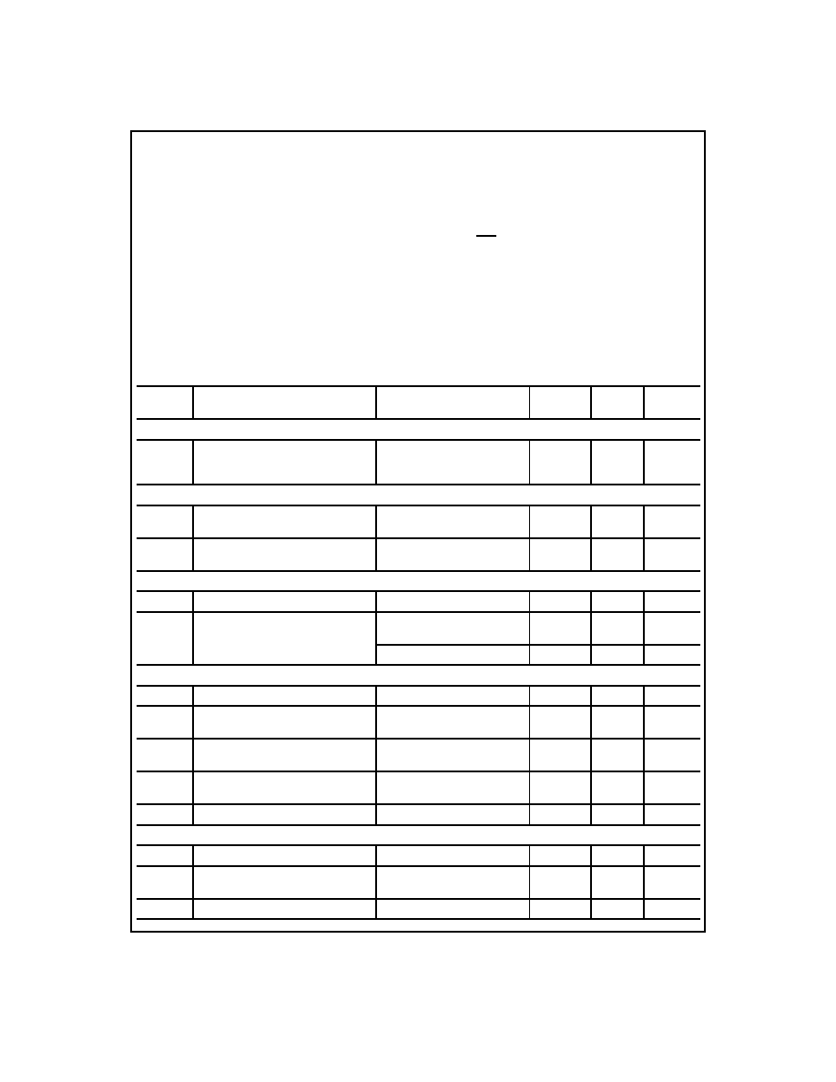
Electrical Characteristics
The following specifications apply for AGND=DGND=0V, V
A
=+5.0V
DC
, V
D
=+3.0 or +5.0V
DC
, f
MCLK
=12MHz. Boldface limits apply
for T
A
=T
J
=T
MIN
to T
MAX
; all other limits T
A
=T
J
=25∞C. (Notes 7, 8, 12 & 16)
Symbol
Parameter
Conditions
Typical
(Note 9)
Limits
(Note 10)
Units
(Limits)
CCD/CIS Source Requirements for Full Specified Accuracy and Dynamic Range (Note 12)
V
OS PEAK
Sensor's Maximum Peak Differential
Signal Range
Gain = 0.933
Gain = 3.0
Gain = 9.0
2.1
0.65
0.21
V
V
V
Full Channel Linearity (In units of 12 bit LSBs) (Note 14)
DNL
Differential Non-Linearity
+0.9
-0.4
+2
-0.9
LSB(max)
INL
Integral Non-Linearity Error (Note 11)
±2.2
+5
-7
LSB(max)
Analog Input Characteristics
OS
R
,
OS
G
,
OS
B
Input Capacitance
5
pF
OS
R
,
OS
G
,
OS
B
Input Leakage Current
Measured with OS = 3.5V
DC
CDS disabled
20
25
µA (max)
CDS enabled
10
nA
Coarse Color Balance PGA Characteristics
Monotonicity
5
bits (min)
G
0
(Minimum PGA Gain)
PGA Setting = 0
0.93
.90
.96
V/V (min)
V/V (max)
G
31
(Maximum PGA Gain)
PGA Setting = 31
3.0
2.95
3.07
V/V (min)
V/V (max)
x3 Boost Gain
x3 Boost Setting On
(Bit 5 of Gain Register is set)
3.0
2.86
3.08
V/V (min)
V/V (max)
Gain Error at any gain (Note 13)
±0.3
1.6
% (max)
Static Offset DAC Characteristics (In units of 12 bit LSBs)
Monotonicity
6
bits (min)
Offset DAC LSB size
PGA gain = 1
18.9
13
24
LSB (min)
LSB (max)
Offset DAC Adjustment Range
PGA gain = 1
±585
±570
LSB (min)
Positive Supply Voltage (V
+
=V
A
=V
D
)
With Respect to
GND
=
AGND
=
DGND
6.5V
Voltage On Any Input or Output Pin
-0.3V to V
+
+0.3V
Input Current at any pin (Note 3)
±25mA
Package Input Current (Note 3)
±50mA
Package Dissipation at T
A
= 25∞C
(Note 4)
ESD Susceptibility (Note 5)
Human Body Model
7000V
Machine Model
450V
Soldering Information
Infrared, 10 seconds (Note 6)
235∞C
Storage Temperature
-65∞C to +150∞C
Operating Temperature Range
T
MIN
=0∞C
T
A
T
MAX
=+70∞C
V
A
Supply Voltage
+4.75V to +5.25V
V
D
Supply Voltage
+3.0V to +5.25V
V
D
-V
A
100mV
OS
R
, OS
G
, OS
B
Input Voltage Range
-0.05V to
A
+ 0.05V
SCLK, SDI, SEN, MCLK, VSMP, CLMP
Input Voltage Range
-0.05V to V
D
+ 0.05V
Absolute Maximum Ratings
(Notes 1& 2)
Operating Ratings
(Notes 1& 2)
4
www.national.com
Symbol
Parameter
Conditions
Typical
(Note 9)
Limits
(Note 10)
Units
(Limits)
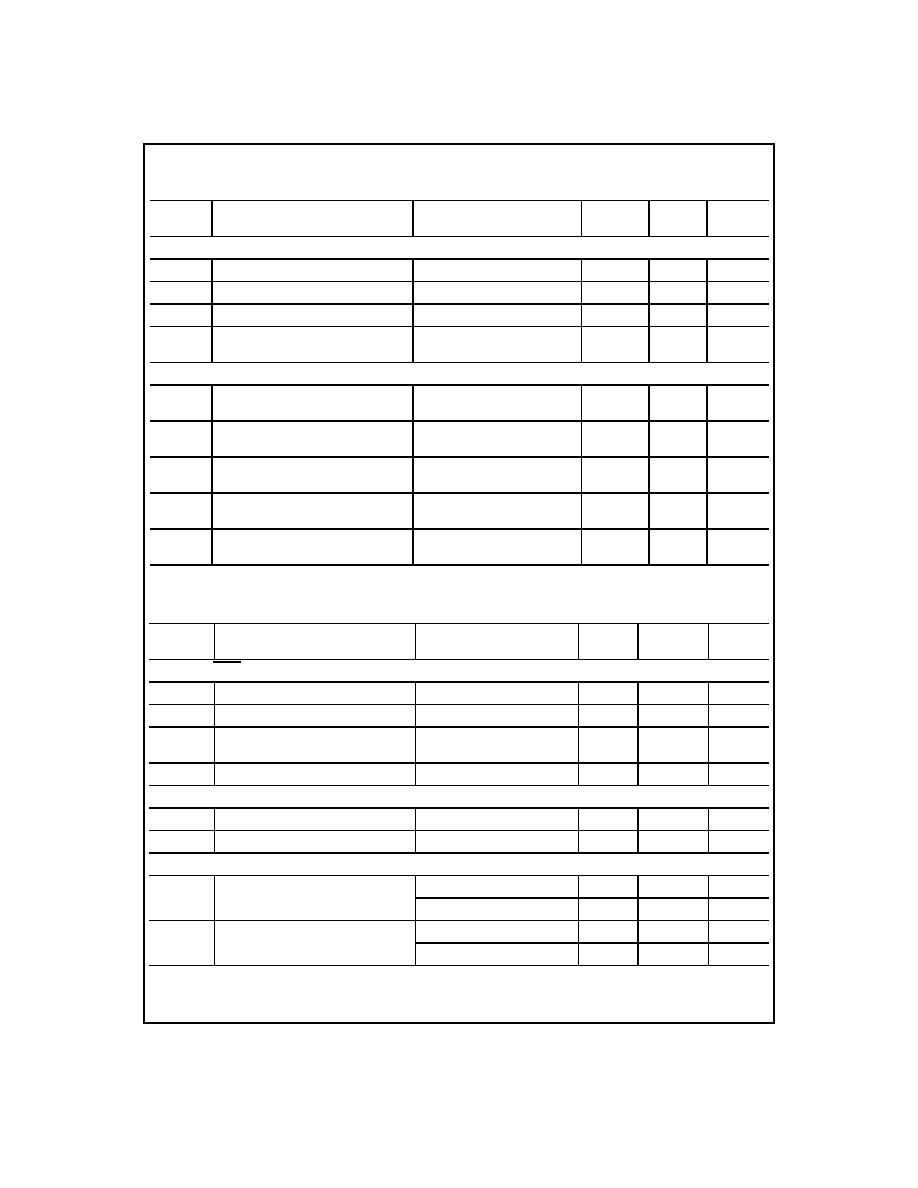
Internal Reference Characteristics
V
REFMID
Mid Reference Output Voltage
2.5
V
V
REF+ OUT
Positive Reference Output Voltage
3.5
V
V
REF- OUT
Negative Reference Output Voltage
1.5
V
V
REF
Differential Reference Voltage
V
REF+ OUT
- V
REF- OUT
2.0
V
System Characteristics (In units of 12 bit LSBs) (see section 5.1, Internal Offsets)
C
Analog Channel Gain Constant
(ADC Codes/V)
Includes voltage reference
variation, gain setting = 1
2107
1934
2281
LSB (min)
LSB (max)
V
OS1
Pre-Boost Analog Channel Offset Error,
CCD Mode
17.3
-61
+94
LSB (min)
LSB (max)
V
OS1
Pre-Boost Analog Channel Offset Error,
CIS Mode
27
-49
+103
LSB (min)
LSB (max)
V
OS2
Pre-PGA Analog Channel Offset Error
-40
-124
+44
LSB (min)
LSB (max)
V
OS3
Post-PGA Analog Channel Offset Error
-38
-130
+55
LSB (min)
LSB (max)
DC and Logic Electrical Characteristics
The following specifications apply for AGND=DGND=0V, V
A
=+5.0V
DC
, V
D
=+3.0 or +5.0V
DC
, f
MCLK
=12MHz. Boldface limits apply
for T
A
=T
J
=T
MIN
to T
MAX
; all other limits
A
=T
J
=25∞C. (Notes 7& 8)
Symbol
Parameter
Conditions
Typical
(Note 9)
Limits
(Note 10)
Units
(Limits)
SCLK, SDI, SEN, MCLK, VSMP, CLMP Digital Input Characteristics
V
IN(1)
Logical "1" Input Voltage
V
A
=5.25V
2.0
V (max)
V
IN(0)
Logical "0" Input Voltage
V
A
=4.75V
0.8
V (min)
I
IN
Input Leakage Current
V
IN
=V
A
V
IN
=DGND
0.1
-0.1
µA(max)
µA(max)
C
IN
Input Capacitance
5
pF
D0-D7 Digital Output Characteristics
V
OUT(1)
Logical "1" Output Voltage
I
OUT
=-360µA
0.8*V
D
V (min)
V
OUT(0)
Logical "0" Output Voltage
I
OUT
=1.6mA
0.2*V
D
V (max)
Power Supply Characteristics
I
A
Analog Supply Current
Operating
75
108
mA (max)
Power Down
675
900
µA (max)
I
D
Digital Supply Current (Note 15)
Operating
210
475
µA (max)
Power Down
2
25
µA (max)
Electrical Characteristics
(Continued)
The following specifications apply for AGND=DGND=0V, V
A
=+5.0V
DC
, V
D
=+3.0 or +5.0V
DC
, f
MCLK
=12MHz. Boldface limits apply
for T
A
=T
J
=T
MIN
to T
MAX
; all other limits T
A
=T
J
=25∞C. (Notes 7, 8, 12 & 16)
5
www.national.com
AC Electrical Characteristics
The following specifications apply for AGND=DGND=0V, V
A
=+5.0V
DC
, V
D
=+3.0 or +5.0V
DC
, f
MCLK
=12MHz, except where noted
otherwise. Boldface limits apply for
A
=T
J
=T
MIN
to T
MAX
; all other limits T
A
=T
J
=25∞C.
(Notes 7& 8)
Note 1: Absolute Maximum Ratings indicate limits beyond which damage to the device may occur. Operating Ratings indicate conditions for which the device is functional,
but do not guarantee specific performance limits. For guaranteed specifications and test conditions, see the Electrical Characte ristics. The guaranteed specifications apply
only for the test conditions listed. Some performance characteristics may degrade when the device is not operated under the list ed test conditions.
Note 2: All voltages are measured with respect to GND=AGND=DGND=0V, unless otherwise specified.
Note 3: When the input voltage (V
IN
) at any pin exceeds the power supplies (V
IN
<GND or V
IN
>V
A
or
V
D
), the current at that pin should be limited to 25mA. The 50m
maximum package input current rating limits the number of pins that can simultaneously safely exceed the power supplies with an input current of 25mA to two.
Note 4: The maximum power dissipation must be derated at elevated temperatures and is dictated by T
J
max,
JA
and the ambient temperature, T
A
. The maximum allow-
able power dissipation at any temperature is P
D
= (T
J
max - T
A
) /
JA
. T
J
max = 150∞C for this device. The typical thermal resistance (
JA
) of this part when board mounted
is 69∞C/W for the M28B SOIC package
.
Note 5: Human body model, 100pF capacitor discharged through a 1.5k
resistor. Machine model, 200 pF capacitor discharged through a 0
resistor.
Note 6: See AN450 "Surface Mounting Methods and Their Effect on Product Reliability" or the section titled "Surface Mount" found in any National Semiconductor Linear
Data Book for other methods of soldering surface mount devices.
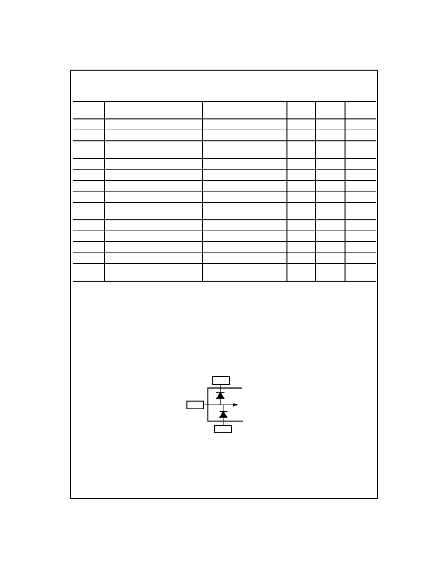
Note 7: Two diodes clamp the OS analog inputs to
AGND
and
V
A as shown below. This input protection, in combination with the external clamp capacitor and the output
impedance of the sensor, prevents damage to the LM9822 from transients during power-up.
Note 8: To guarantee accuracy, it is required that V
A
and V
D
be connected to clean, low noise power supplies, with separate bypass capacitors at each supply pin. When
both V
A
and V
D
are operated at 5.0V, they must be powered by the same regulator, with separate power planes or traces and separate bypass capacitors at each supply pin.
Symbol
Parameter
Conditions
Typical
(Note 9)
Limits
(Note 10)
Units
(Limits)
f
MCLK
Maximum MCLK frequency
12
MHz (min)
t
MCLK
MCLK period
83
ns (min)
MCLK duty cycle
40
60
%(min)
%(max)
t
SCLK
Serial Clock Period
1
t
MCLK
(min)
t
SEN
Serial Enable high time
3
t
MCLK
(min)
t
SSU
SDI setup time
1
ns (min)
t
SH
SDI hold time
3
ns (min)
t
SDDO
SCLK
edge to new valid data
V
D
= 5.0V
V
D
= 3.3V
8.5
19
20
ns (max)
t
VSU
VSMP setup time
1
ns (min)
t
VH
VSMP hold time
3
ns (min)
t
CSU
CLMP setup time
1
ns (min)
t
CH
CLMP hold time
3
ns (min)
t
DDO
MCLK
edge to new valid data
V
D
= 5.0V
V
D
= 3.3V
16
25
25
ns (max)
ns (max)
OS Input
AGND
V
A
TO INTERNAL
CIRCUITRY