Äîêóìåíòàöèÿ è îïèñàíèÿ www.docs.chipfind.ru
1
www.national.com
General Description
The LM9831 is a complete USB image scanner system on a sin-
gle IC. The LM9831 provides all the functions (image sensor
control, illumination control, analog front end, pixel processing
function image data buffer/DRAM controller, microstepping
motor controller, and USB interface) necessary to create a high
performance color scanner. The LM9831 scans images in 42 bit
color/14 bit gray, and has output data formats for 24 bit color/8
bit gray. The LM9831 supports sensors with pixel counts of up to
16384 pixels x 3 colors (1200 dpi x 13.6 inches).
The LM9831's low operating and suspend mode supply currents
allow design of USB bus-powered scanners. The only additional
active components required are an external 4Mbit or 16Mbit
DRAM for data buffering and power transistors for the stepper
motor.
Applications
·
Color Flatbed Document Scanners
·
Color Sheetfed Document Scanners
Features
· 14 bit ADC digitizes at up to 6Mpixels/s (2M RGB pixels/sec).
· Digital Pixel Processing provides 1200, 800, 600, 400, 300,
200, 150, and 100dpi horizontal resolution from a 1200dpi
sensor and 600, 400, 300, 200, 150, 100, 75, and 50dpi
horizontal resolution from a 600dpi sensor.
· Provides 50-2400dpi vertical resolution in 1 dpi increments.
· Pixel rate error correction for gain (shading) and offset errors.
· Supports 4 or 16Mbit external DRAMs.
· Multiple CCD clocking rates allows matching of CCD clock to
scan resolution and pixel depth for maximum scan speed.
· Stepper motor control tightly coupled with image data buffer
management to maximize data transfer efficiency.
· PWM stepper motor current control allows microstepping for
the price of fullstepping.
· USB interface for Plug and Play operation on USB-equipped
computers.
· Serial EEPROM option for custom Vendor and Product IDs.
· Support for USB bus-powered operation.
· Pixel depths of 1, 2, or 4 bits are packed into bytes for faster
scans of line art and low pixel depth images.
· Supports 3 channel CCDs and 1 channel CIS sensors.
· 3 (R, G, and B) 12-bit, user-programmable gamma correction
tables.
· Compatible with a wide range of color linear CCDs and
Contact Image Sensors (CIS).
· Operates with 48MHz external crystal.
· Internal bandgap voltage reference.
· 100 pin TQFP package
Key Specifications
·
Analog to Digital Converter Resolution
14 Bits
·
Maximum Pixel Conversion Rate
6MHz
·
A4 Color 150dpi scan time
<10 seconds
·
A4 Color 300dpi scan time
<40 seconds
·
A4 Color 600dpi scan time
<160 seconds
·
Supply Voltage
- LM9831
+4.75V to +5.25V
- LM9831 DRAM I/O
+2.85 to +5.25V
·
Typical Operating Current Consumption
134mA
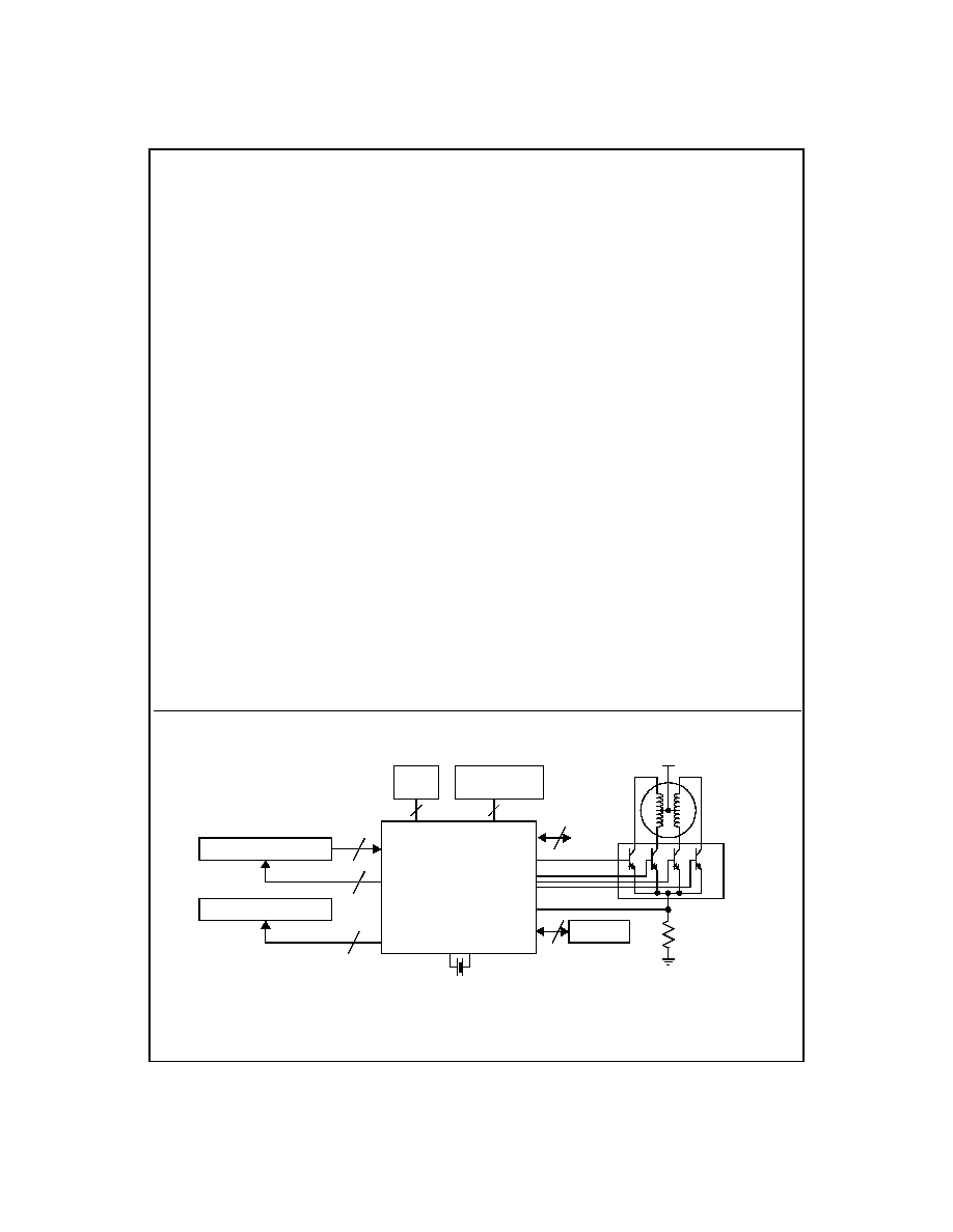
LM9831 42-Bit Color, 1200dpi USB Image Scanner
LM9831 Scanner System Block Diagram
CCD/CIS
Illumination
+24V
Stepper
Motor
1-3
1-3
2-6
Power
Transistors
DRAM
30
LM9831CCVJD
USB
Port
2
48MHz Crystal
Optional Serial
EEPROM
2
8
MISC
I/O
LM
98
31
42
-B
it
C
o
lo
r
120
0d
pi
U
S
B
Im
a
g
e
S
c
a
n
n
e
r
©1999 National Semiconductor Corporation
TRI-STATE® is a registered trademark of National Semiconductor Corporation.
October 1999
N

2
www.national.com
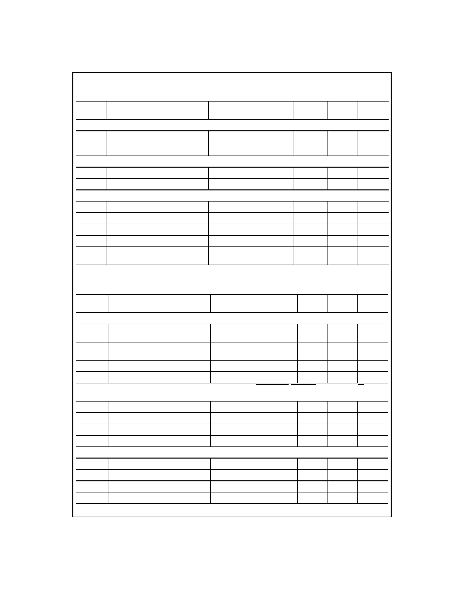
Electrical Characteristics
The following specifications apply for AGND=DGND=0V, V
A
=V
D
=V
DRAM
=+5.0V
DC
,
f
CRYSTAL IN
= 48MHz. Boldface limits apply for T
A
=T
J
=T
MIN
to T
MAX
; all other limits T
A
=T
J
=25°C. (Notes 8, 9, & 10)
Symbol
Parameter
Conditions
Typical
(Note 9)
Limits
(Note 10)
Units
(Limits)
Full Channel Characteristics (in units of 12 bit LSBs unless otherwise noted)
Resolution with No Missing Codes
14
12
bits (min)
DNL
Differential Non-Linearity
V
DRAM
=3.3V
-0.47
+0.95
-1
+2.4
LSB (min)
LSB (max)
INL
Integral Non-Linearity Error (Note 11)
V
DRAM
=3.3V
-3.2
+2.6
-12.6
+7.3
LSB (min)
LSB (max)
C
Analog Channel Gain Constant
(ADC Codes/V), referred to 14 bits.
Includes voltage reference
variation, gain setting = 1
8192
7412
9300
LSB (min)
LSB (max)
V
OS1
Pre-Boost Analog Channel Offset Error
26
-34
+76
mV (min)
mV (max)
V
OS2
Pre-PGA Analog Channel Offset Error
-30
-80
+31
mV (min)
mV (max)
V
OS3
Post-PGA Analog Channel Offset Error
-26
-75
+26
mV (min)
mV (max)
Coarse Color Balance PGA Characteristics (Configuration Registers 3B, 3C, and 3D)
Monotonicity
5
bits (min)
G
0
(Minimum PGA Gain)
PGA Setting = 0
0.93
0.90
0.96
V/V (min)
V/V (max)
G
31
(Maximum PGA Gain)
PGA Setting = 31
3.00
2.95
3.05
V/V (min)
V/V (max)
x3 Boost Gain
x3 Boost Setting On
(bit B5 of Gain Register is set)
2.94
2.85
3.04
V/V (min)
V/V (max)
Gain Error at any gain (Note 13)
0.3
-0.6
+0.9
% (min)
% (max)
Static Offset DAC Characteristics (Configuration Registers 38, 39, and 3A)
Monotonicity
6
bits (min)
Offset DAC LSB size
PGA gain = 1
9
6
12
mV (min)
mV (max)
Offset DAC Adjustment Range
PGA gain = 1
±278
±256
mV (min)
Positive Supply Voltage (V
+
=V
A
=V
D
=V
DRAM
)
With Respect to GND=AGND=DGND
6.5V
Voltage On Any Input or Output Pin
-0.3V to V
+
+0.3V
Input Current at any pin (Note 3)
±25mA
Package Input Current (Note 3)
±50mA
Package Dissipation at T
A
= 25°C
(Note 4)
ESD Susceptibility (Note 5)
Human Body Model
2000 V
Machine Model
250 V
Soldering Information
Infrared, 10 seconds (Note 6)
235°C
Storage Temperature
-65°C to +150°
Operating Temperature Range
T
MIN
T
A
T
MAX
LM9831VJD
0°C
T
A
+70°C
V
A
Supply Voltage
+4.75V to +5.25V
V
D
Supply Voltage
+4.75V to +5.25V
V
DRAM
Supply Voltage
+2.85V
V
DRAM
V
D
+100mV
|V
A
-V
D
|
100mV
Input Voltage Range
-0.05V to V
+
+ 0.05V
Absolute Maximum Ratings
(Notes 1 & 2)
Operating Ratings
(Notes 1 & 2)
3
www.national.com
CCD/CIS Source Requirements for Full Specified Accuracy and Dynamic Range (Note 12)
V
CCDPEAK
Sensor's Maximum Output Signal
Amplitude before LM9831 Analog Front
End Saturation
Gain = 0.933
Gain = 3.0
Gain = 9.0
1.9
0.6
0.19
V
V
V
Analog Input Characteristics
Average OS
R
, OS
G
, OS
B
Input Current
CDS Enabled, OS = 3.5V
DC
±3
nA
OS
R
, OS
G
, OS
B
Input Current
CDS Disabled, OS = 3.5V
DC
±26
±30
µA (max)
Internal Voltage Reference Characteristics
V
BANDGAP
Voltage Reference Output Voltage
1.23
V
V
REF LO
Negative Reference Output Voltage
V
REF MID
-1.0
V
V
REF MID
Midpoint Reference Output Voltage
V
A
/2.0
V
V
REF HI
Positive Reference Output Voltage
V
REF MID
+1.0
V
V
REGULA-
TOR
USB I/O Voltage Regulator
3.4
V
DC and Logic Electrical Characteristics
The following specifications apply for AGND=DGND=0V, V
A
=V
D
=V
DRAM
=+5.0V
DC
unless otherwise noted,
f
CRYSTAL IN
= 48MHz. Boldface limits apply for T
A
=T
J
=T
MIN
to T
MAX
; all other limits T
A
=T
J
=25°C. (Notes 8, 9, & 10)
Symbol
Parameter
Conditions
Typical
(Note 9)
Limits
(Note 10)
Units
(Limits)
Digital Input Characteristics for D0-D15 (DRAM Interface)
V
IN(1)
Logical "1" Input Voltage
V
DRAM
=5.25V
V
DRAM
=3.6V
2.0
2.0
V (min)
V (min)
V
IN(0)
Logical "0" Input Voltage
V
DRAM
=4.75V
V
DRAM
=2.85V
0.8
0.8
V (max)
V (max)
I
IN
Input Leakage Current
±0.1
µA
C
IN
Input Capacitance
5
pF
Digital Input Characteristics for PAPER SENSE 1-2, MISC I/O 1-6, SDA, BUS POWER, CRYSTAL/EXT CLOCK, 24/48, RESET,
CMODE
V
IN(1)
Logical "1" Input Voltage
V
D
=5.25V
2.0
V (min)
V
IN(0)
Logical "0" Input Voltage
V
D
=4.75V
0.8
V (max)
I
IN
Input Leakage Current
±0.1
µA
C
IN
Input Capacitance
5
pF
Digital Input Characteristics for D+, D-
V
IN(1)
Logical "1" Input Voltage
V
D
=5.25V
2.0
V (min)
V
IN(0)
Logical "0" Input Voltage
V
D
=4.75V
0.8
V (max)
I
IN
Input Leakage Current
±0.1
µA
C
IN
Input Capacitance
5
pF
Electrical Characteristics
(Continued)
The following specifications apply for AGND=DGND=0V, V
A
=V
D
=V
DRAM
=+5.0V
DC
,
f
CRYSTAL IN
= 48MHz. Boldface limits apply for T
A
=T
J
=T
MIN
to T
MAX
; all other limits T
A
=T
J
=25°C. (Notes 8, 9, & 10)
Symbol
Parameter
Conditions
Typical
(Note 9)
Limits
(Note 10)
Units
(Limits)
4
www.national.com
Digital Output Characteristics for D0-D15, A0-A9, RD, WR, RAS, CAS (DRAM Interface)
V
OUT(1)
Logical "1" Output Voltage
V
DRAM
=4.75V, I
OUT
=-4mA
V
DRAM
=2.85V, I
OUT
=-4mA
2.4
2.4
V (min)
V (min)
V
OUT(0)
Logical "0" Output Voltage
V
DRAM
=4.75V, I
OUT
=4mA
V
DRAM
=2.85V, I
OUT
=4mA
0.4
0.4
V (max)
V (max)
Digital Output Characteristics for A, B, A, B
V
OUT(1)
Logical "1" Output Voltage
V
DRAM
=4.75V, I
OUT
=-10mA
V
DRAM
=2.85V, I
OUT
=-10mA
2.4
2.4
V (min)
V (min)
V
OUT(0)
Logical "0" Output Voltage
V
DRAM
=4.75V, I
OUT
=4mA
V
DRAM
=2.85V, I
OUT
=4mA
0.4
0.4
V (max)
V (max)
Digital Output Characteristics for MISC I/O 1-6, TR1, TR2, ø1, ø2, RS, CP1, CP2, LAMP
R
, LAMP
G
, LAMP
B
V
OUT(1)
Logical "1" Output Voltage
V
D
=4.75V, I
OUT
=-4mA
2.4
V (min)
V
OUT(0)
Logical "0" Output Voltage
V
D
=4.75V, I
OUT
=4mA
0.4
V (max)
Digital Output Characteristics for D+, D-
V
OUT(1)
Logical "1" Output Voltage
V
D
=4.75V, I
OUT
=-1mA
2.4
V (min)
V
OUT(0)
Logical "0" Output Voltage
V
D
=4.75V, I
OUT
=3mA
0.4
V (max)
CRYSTAL IN, CRYSTAL OUT Characteristics
XTAL
OUT DC
CRYSTAL OUT Bias Level (Offset)
0.8
V
XTAL
OUT AC
CRYSTAL OUT Amplitude
f
CRYSTAL
= 48MHz
0.8
V
P-P
Power Supply Characteristics
I
A
Analog Supply Current
(V
A
pins)
Operating
Suspend
87
1
137
mA (max)
µA (max)
I
D
Digital Supply Current
(V
D
pins)
Operating
Suspend (including I
DRAM
)
37
14
50
mA (max)
µA (max)
I
DRAM
DRAM Supply Current
(V
DRAM
pins)
Operating, V
DRAM
= 5V
Operating, V
DRAM
= 3V
Suspend
10
5
14
21
14
mA (max)
mA (max)
µA (max)
DC and Logic Electrical Characteristics
(Continued)
The following specifications apply for AGND=DGND=0V, V
A
=V
D
=V
DRAM
=+5.0V
DC
unless otherwise noted,
f
CRYSTAL IN
= 48MHz. Boldface limits apply for T
A
=T
J
=T
MIN
to T
MAX
; all other limits T
A
=T
J
=25°C. (Notes 8, 9, & 10)
Symbol
Parameter
Conditions
Typical
(Note 9)
Limits
(Note 10)
Units
(Limits)
5
www.national.com
Note 1: Absolute Maximum Ratings indicate limits beyond which damage to the device may occur. Operating Ratings indicate conditions for which the device is functional,
but do not guarantee specific performance limits. For guaranteed specifications and test conditions, see the Electrical Characteristics. The guaranteed specifications apply
only for the test conditions listed. Some performance characteristics may degrade when the device is not operated under the listed test conditions.
Note 2: All voltages are measured with respect to GND=AGND=DGND=0V, unless otherwise specified.
Note 3: When the input voltage (V
IN
) at any pin exceeds the power supplies (V
IN
<GND or V
IN
>V
A
or V
D
), the current at that pin should be limited to 25mA. The 50mA
maximum package input current rating limits the number of pins that can simultaneously safely exceed the power supplies with an input current of 25mA to two.
Note 4: The maximum power dissipation must be derated at elevated temperatures and is dictated by T
J
max,
JA
and the ambient temperature, T
A
. The maximum allow-
able power dissipation at any temperature is P
D
= (T
J
max - T
A
) /
JA
. T
J
max = 150°C for this device. The typical thermal resistance (
JA
) of this part when board mounted
is 53°C/W
.
Note 5: Human body model, 100pF capacitor discharged through a 1.5k
resistor. Machine model, 200pF capacitor discharged through a 0
resistor.
Note 6: See AN-450 "Surface Mounting Methods and Their Effect on Product Reliability" or the section titled "Surface Mount" found in any National Semiconductor Linear
Data Book for other methods of soldering surface mount devices.
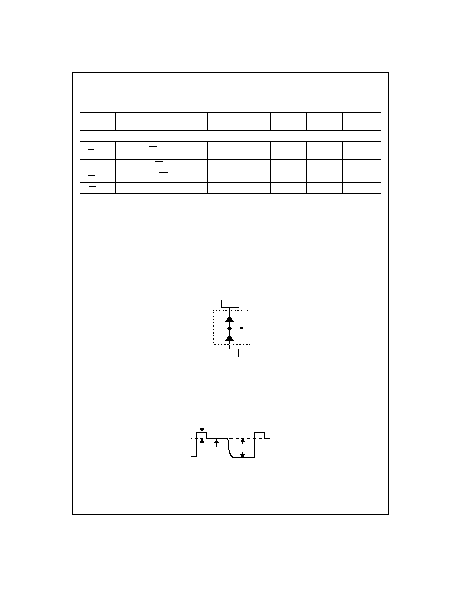
Note 7: Two diodes clamp the OS analog inputs to
AGND
and
VA
as shown below. This input protection, in combination with the external clamp capacitor and the output
impedance of the sensor, prevents damage to the LM9831 from transients during power-up.
Note 8: For best performance, it is required that all supply pins be powered from the same power supply with separate bypass capacitors at each supply pin.
Note 9: Typicals are at T
J
=T
A
=25°C, f
CRYSTAL IN
= 48MHz, and represent most likely parametric norm.
Note 10: Tested limits are guaranteed to National's AOQL (Average Outgoing Quality Level).
Note 11: Integral linearity error is defined as the deviation of the analog value, expressed in LSBs, from the straight line that best fits the actual transfer function of the ADC.
Note 12: V
REF
is defined as the CCD OS voltage for the reference period following the reset feedthrough pulse. V
WHITE
is defined as the peak CCD pixel output voltage for
a white (full scale) image with respect to the reference level, V
REF
. V
RFT
is defined as the peak positive deviation above V
REF
of the reset feedthrough pulse. The maximum
correctable range of pixel-to-pixel V
WHITE
variation is defined as the maximum variation in V
WHITE
(due to PRNU, light source intensity variation, optics, etc.) that the
LM9831 can correct for using its internal PGA.
Note 13: PGA Gain Error is the maximum difference between the measured gain for any PGA code and the ideal gain calculated by using the formula
where
.
AC Electrical Characteristics
The following specifications apply for AGND=DGND=0V, V
A
=V
D
=V
DRAM
=+5.0V
DC
unless otherwise noted,
f
CRYSTAL IN
= 48MHz, MCLK DIVIDER = 1.0 (unless otherwise noted), f
MCLK
= f
CRYSTAL IN
/MCLK DIVIDER, f
ADC CLK
= f
MCLK
/8,
C
L
(databus loading) = 20pF/pin. Boldface limits apply for T
A
=T
J
=T
MIN
to T
MAX
; all other limits T
A
=T
J
=25°C. (Notes 8, 9, & 10)
Symbol
Parameter
Conditions
Typical
(Note 9)
Limits
(Note 10)
Units
(Limits)
DRAM Timing (Figure 1)
t
RD SETUP
Data valid to RD rising edge
V
DRAM
=5.0V
V
DRAM
=3.3V
26
35
ns (min)
ns (min)
t
RD HOLD
Data valid after RD rising edge
0
ns (min)
t
WR SETUP
Data valid before WR falling edge
5
ns (min)
t
WR HOLD
Data valid after WR rising edge
10
ns (min)
OS Input
AGND
VA
To Internal
Circuitry
V
WHITE
V
REF
V
RFT
CCD Output Signal
Gain
PGA
V
V
----
G
0
X
PGA code
32
---------------------------
+
=
X
G
31
G
0
(
)
32
31
------
=