LM98501
10-Bit, 27 MSPS Camera Signal Processor
General Description
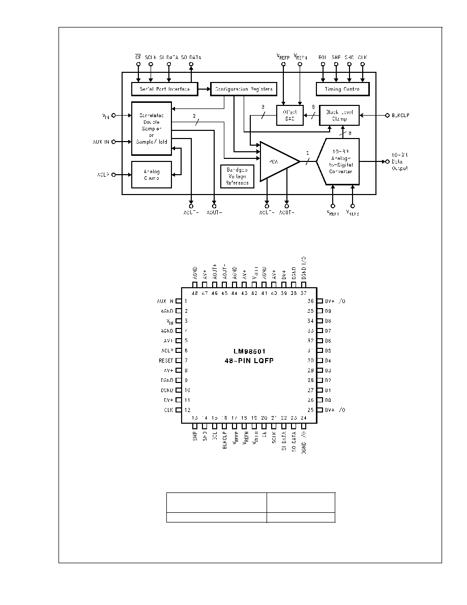
The LM98501 is a CCD signal processor for electronic cam-
eras. The processor provides a common interface to a num-
ber of different image sensors including CCD, CMOS, and
CIS. Correlated double sampling reduces kTC noise from
the image signal. A fast, temperature stable, 8-bit digitally
programmable
gain
amplifier
enables
pixel-rate
white-balancing. An auxiliary input is provided, allowing for
the selection of an external signal, useful for electronic titling
and video overlay. The 10-bit A/D converter preserves the
image quality with excellent noise performance. The
LM98501 also includes the supporting functions of digital
black level clamp and power down, ideally suited for portable
video applications. This low-power processor is a natural
choice for the most demanding imaging systems.
Applications
n
Digital still camera
n
Digital video camcorder
n
Video conferencing
n
Security camera
n
Plain paper copier
n
Flatbed or handheld color scanner
n
Video processing for x-ray or infrared
n
Barcode scanner
Features
n
+3V single power supply
n
Low power CMOS design
n
4-wire serial interface
n
2.5V data output voltage swing
n
No missing codes
n
AUX input with input clamp and programmable gain
n
Four color gain and offset registers
n
Digital black level clamp
n
Small 48-lead LQFP package
Key Specifications
j
Maximum Input Level
1.0V peak-peak
j
CDS Sampling Rate
27 MSPS
j
PGA Gain Steps
256 Steps
j
PGA Gain Range
0.0 dB-32.0 dB
j
ADC Resolution
10-Bit
j
ADC Sampling Rate
27 MSPS
j
*Signal-to-Noise Ratio
60 dB 0 dB Gain, 1.0V Input
j
Power Dissipation
AV+ = DV+ = DV+ I/O = 3.0V
195 mW (typical)
j
Operating Temperature
0∞C to 70∞C
*
20 log
10
(V
IN
/RMS Output Noise)
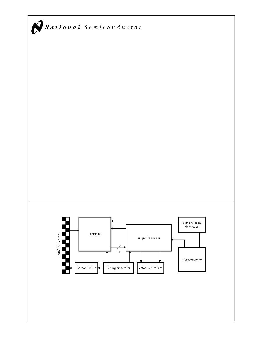
Typical Digital Camera Block Diagram
DS101292-1
February 2000
LM98501
10-Bit,
27
MSPS
Camera
Signal
Processor
© 2000 National Semiconductor Corporation
DS101292
www.national.com
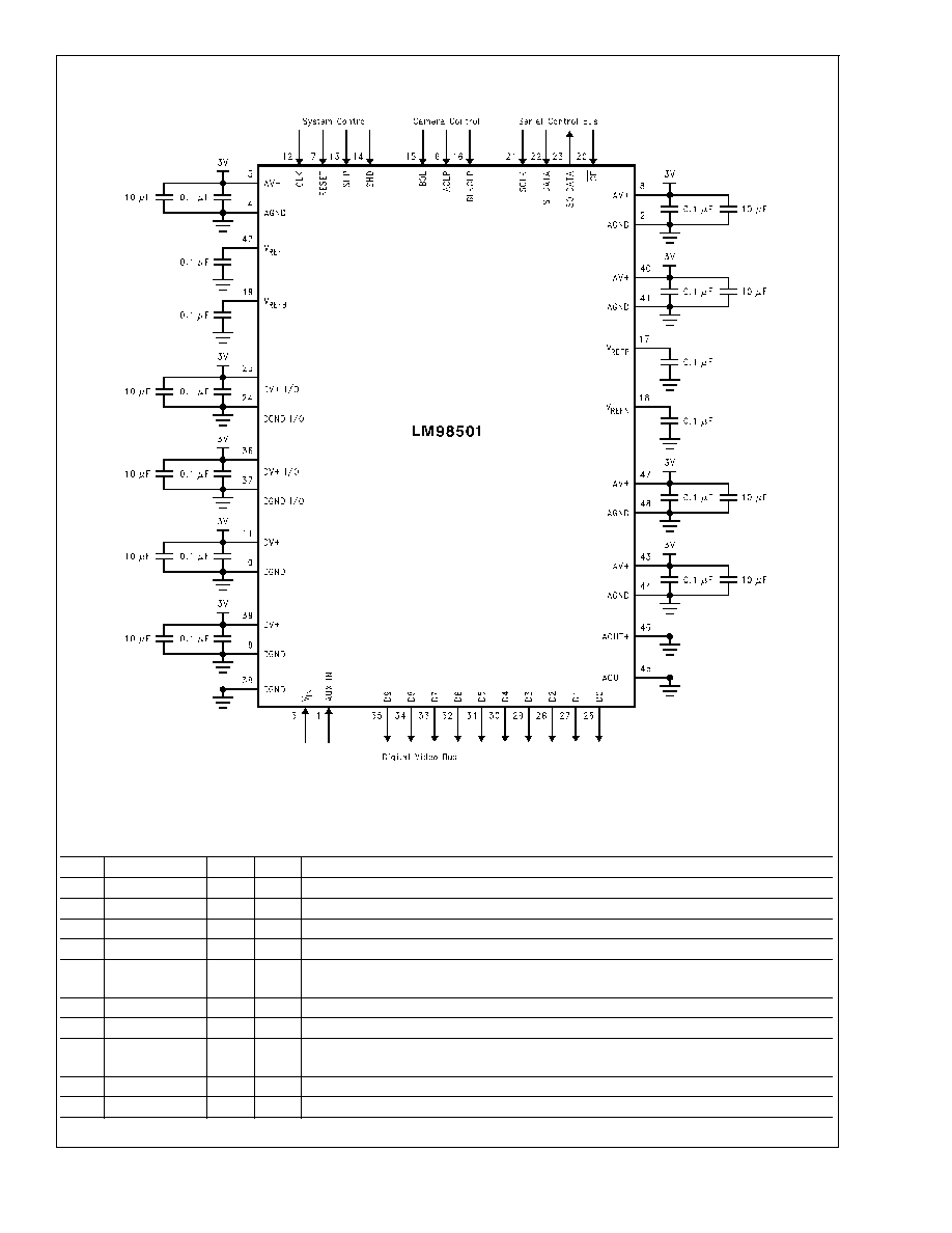
Typical Application Circuit
Pin Descriptions
Pin
Name
I/O
Typ
Description
1
AUX IN
I
A
Auxiliary analog input.
2
AGND
P
Analog ground return.
3
V
IN
I
A
Analog input. AC-couple input signal through a 0.1 µF capacitor
4
AGND
P
Analog ground return.
5
AV+
P
+3V power supply for the analog circuits. Bypass each supply pin with 0.1 µF and
10 µF capacitors in parallel.
6
ACLP
I
D
Analog clamp switch. Float pin when function not being used.
7
RESET
I
D
Active-high master reset. Float pin when function not being used.
8
AV+
P
+3V power supply for the analog circuits. Bypass each supply pin with 0.1 µF and
10 µF capacitors in parallel.
9
DGND
P
Digital ground return.
10
DGND
P
Digital ground return.
DS101292-4
FIGURE 3. Typical Application Circuit Diagram
LM98501
www.national.com
3

Pin Descriptions
(Continued)
Pin
Name
I/O
Typ
Description
11
DV+
P
+3V power supply for the digital circuits. Bypass each supply pin with 0.1 µF and
10 µF capacitors in parallel.
12
CLK
I
D
27 MHz clock input.
13
SHP
I
D
Correlated double sampler reset voltage clamp override. Programmable active-high or
active-low through serial interface. Connect to +3V digital supply when function not
being used (register values in default condition).
14
SHD
I
D
Correlated double sampler video signal voltage sample override. Programmable
active-high or active-low through serial interface. Connect to +3V digital supply when
function not being used (register values in default condition).
15
BOL
I
D
Active-high beginning of line switch input. Hold high during entire line of effective
pixels. Hold low during blanking period.
16
BLKCLP
I
D
Active-high black level clamp switch input. Pulse high during black pixels to eliminate
black pixel offset from video signal.
17
V
REFP
IO
A
Top of DAC reference ladder. Normally bypassed with a 0.1 µF capacitor. An external
DAC reference voltage may be applied to this pin.
18
V
REFN
IO
A
Bottom of DAC reference ladder. Normally bypassed with a 0.1 µF capacitor. An
external DAC reference voltage may be applied to this pin.
19
V
REFB
IO
A
Bottom of ADC reference ladder. Normally bypassed with a 0.1 µF capacitor. An
external ADC reference voltage may be applied to this pin.
20
CE
I
D
Active-low chip enable for the serial interface.
21
SCLK
I
D
Serial interface clock used to decode the serial input data.
22
SI DATA
I
D
Serial interface input port.
23
SO DATA
O
D
Serial interface output port.
24
DGND I/O
P
Digital output driver ground return.
25
DV+ I/O
P
+3V power supply for the digital output driver circuits. Bypass each supply pin with
0.1 µF and 10 µF capacitors in parallel.
26
D0
O
D
Digital output. Bit 0 of 9 (LSB) of the digital video output bus.
27
D1
O
D
Digital output. Bit 1 of 9 of the digital video output bus.
28
D2
O
D
Digital output. Bit 2 of 9 of the digital video output bus.
29
D3
O
D
Digital output. Bit 3 of 9 of the digital video output bus.
30
D4
O
D
Digital output. Bit 4 of 9 of the digital video output bus.
31
D5
O
D
Digital output. Bit 5 of 9 of the digital video output bus.
32
D6
O
D
Digital output. Bit 6 of 9 of the digital video output bus.
33
D7
O
D
Digital output. Bit 7 of 9 of the digital video output bus.
34
D8
O
D
Digital output. Bit 8 of 9 of the digital video output bus.
35
D9
O
D
Digital output. Bit 9 of 9 (MSB) of the digital video output bus.
36
DV+ I/O
P
+3V power supply for the digital output driver circuits. Bypass each supply pin with
0.1 µF and 10 µF capacitors in parallel.
37
DGND I/O
P
Digital output driver ground return.
38
DGND
P
Digital ground return.
39
DV+
P
+3V power supply for the digital circuits. Bypass each supply pin with 0.1 µF and 10
µF capacitors in parallel.
40
AV+
P
+3V power supply for the analog circuits. Bypass each supply pin with 0.1 µF and 10
µF capacitors in parallel.
41
AGND
P
Analog ground return.
42
V
REFT
IO
A
Top of ADC reference ladder. Normally bypassed with a 0.1 µF capacitor. An external
ADC reference voltage may be applied to this pin.
43
AV+
P
+3V power supply for the analog circuits. Bypass each supply pin with 0.1 µF and 10
µF capacitors in parallel.
44
AGND
P
Analog ground return.
45
AOUT-
O
A
Negative differential analog output from correlated double sampler or PGA (selectable
through the serial interface).
LM98501
www.national.com
4

Pin Descriptions
(Continued)
Pin
Name
I/O
Typ
Description
46
AOUT+
O
A
Positive differential analog output from correlated double sampler or PGA (selectable
through the serial interface).
47
AV+
P
+3V power supply for the analog circuits. Bypass each supply pin with 0.1 µF and 10
µF capacitors in parallel.
48
AGND
P
Analog ground return.
Legend: (I = Input), (O = Output), (IO = Bi-directional), (P = Power), (D = Digital), (A = Analog).
LM98501
www.national.com
5