LM98714
Three Channel, 16-Bit, 45 MSPS Digital Copier Analog
Front End with Integrated CCD/CIS Sensor Timing
Generator and LVDS Output
General Description
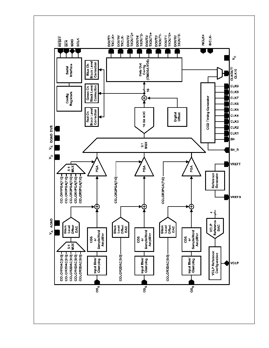
The LM98714 is a fully integrated, high performance 16-Bit,
45 MSPS signal processing solution for digital color copiers,
scanners, and other image processing applications. High-
speed signal throughput is achieved with an innovative ar-
chitecture utilizing Correlated Double Sampling (CDS), typi-
cally employed with CCD arrays, or Sample and Hold (S/H)
inputs (for Contact Image Sensors and CMOS image sen-
sors). The signal paths utilize 8 bit Programmable Gain
Amplifiers (PGA), a +/-9-Bit offset correction DAC and inde-
pendently controlled Digital Black Level correction loops for
each input. The PGA and offset DAC are programmed inde-
pendently allowing unique values of gain and offset for each
of the three inputs. The signals are then routed to a 45MHz
high performance analog-to-digital converter (ADC). The
fully differential processing channel shows exceptional noise
immunity, having a very low noise floor of -74dB. The 16-bit
ADC has excellent dynamic performance making the
LM98714 transparent in the image reproduction chain.
Applications
n
Multi-Function Peripherals
n
Facsimile Equipment
n
Flatbed or Handheld Color Scanners
n
High-speed Document Scanner
Features
n
LVDS/CMOS Outputs
n
LVDS/CMOS Pixel Rate Input Clock or ADC Input Clock
n
CDS or S/H Processing for CCD or CIS sensors
n
Independent Gain/Offset Correction for Each Channel
n
Digital Black Level Correction Loop for Each Channel
n
Programmable Input Clamp Voltage
n
Flexible CCD/CIS Sensor Timing Generator
Key Specifications
n
Maximum Input Level
1.2 or 2.4 Volt Modes
n
(both with + or - polarity option)
n
ADC Resolution
16-Bit
n
ADC Sampling Rate
45 MSPS
n
INL
+/- 23 LSB (typ)
n
Channel Sampling Rate
15/22.5/30 MSPS
n
PGA Gain Steps
256 Steps
n
PGA Gain Range
0.7 to 7.84x
n
Analog DAC Resolution
+/-9 Bits
n
Analog DAC Range
+/-300mV or +/-600mV
n
Digital DAC Resolution
+/-6 Bits
n
Digital DAC Range
-1024 LSB to + 1008 LSB
n
SNR
-74dB (
@
0dB PGA Gain)
n
Power Dissipation
505mW (LVDS) 610mW (CMOS)
n
Operating Temp
0 to 70�C
n
Supply Voltage
3.3V Nominal (3.0V to 3.6V range)
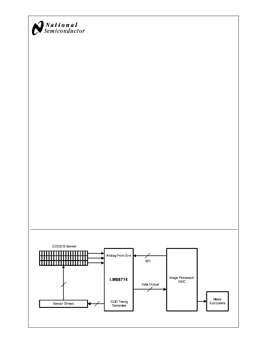
System Block Diagram
20105370
October 2006
LM98714
-
Three
Channel,
16-Bit,
45
MSPS
Digital
Copier
Analog
Front
End
with
Integrated
CCD/CIS
Sensor
T
iming
Generator
and
L
VDS
Output
� 2006 National Semiconductor Corporation
DS201053
www.national.com

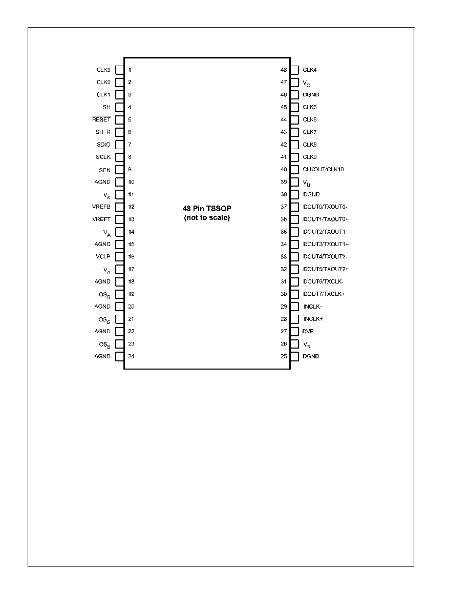
Pin Descriptions
Pin
Name
I/O
Typ
Res
Description
1
CLK3
O
D
PU
Configurable sensor control output.
2
CLK2
O
D
PD
Configurable sensor control output.
3
CLK1
O
D
PU
Configurable sensor control output.
4
SH
O
D
PD
Sensor - Shift or transfer control signal for CCD and CIS sensors.
5
RESET
I
D
PU
Active-low master reset. NC when function not being used.
6
SH_R
I
D
PD
External request for an SH pulse.
7
SDIO
I/O
D
Serial Interface Data Input
8
SCLK
I
D
PD
Serial Interface shift register clock.
9
SEN
I
D
PU
Active-low chip enable for the Serial Interface.
10
AGND
P
Analog ground return.
11
V
A
P
Analog power supply. Bypass voltage source with 4.7�F and pin with 0.1�F to
AGND.
12
VREFB
O
A
Bottom of ADC reference. Bypass with a 0.1�F capacitor to ground.
13
VREFT
O
A
Top of ADC reference. Bypass with a 0.1�F capacitor to ground.
14
V
A
P
Analog power supply. Bypass voltage source with 4.7�F and pin with 0.1�F to
AGND.
15
AGND
P
Analog ground return.
16
VCLP
IO
A
Input Clamp Voltage. Normally bypassed with a 0.1�F, and a 4.7�F capacitor to
AGND. An external reference voltage may be applied to this pin.
17
V
A
P
Analog power supply. Bypass voltage source with 4.7�F and pin with 0.1�F to
AGND.
18
AGND
P
Analog ground return.
19
OS
R
I
A
Analog input signal. Typically sensor Red output AC-coupled thru a capacitor.
20
AGND
P
Analog ground return.
21
OS
G
I
A
Analog input signal. Typically sensor Green output AC-coupled thru a capacitor.
22
AGND
P
Analog ground return.
23
OS
B
I
A
Analog input signal. Typically sensor Blue output AC-coupled thru a capacitor.
24
AGND
P
Analog ground return.
25
DGND
P
Digital ground return.
26
V
R
P
Power supply input for internal voltage reference generator. Bypass this supply
pin with a 0.1�F capacitor.
27
DVB
O
P
Digital Core Voltage bypass. Not an input. Bypass with 0.1�F capacitor to
DGND.
28
INCLK+
I
D
Clock Input. Non-Inverting input for LVDS clocks or CMOS clock input. CMOS
clock is selected when pin 29 is held at DGND, otherwise clock is configured
for LVDS operation.
29
INCLK-
I
D
Clock Input. Inverting input for LVDS clocks, connect to DGND for CMOS clock.
30
DOUT7/
O
D
Bit 7 of the digital video output bus in CMOS Mode, LVDS Frame Clock+ in
LVDS Mode.
TXCLK+
31
DOUT6/
O
D
Bit 6 of the digital video output bus in CMOS Mode, LVDS Frame Clock- in
LVDS Mode.
TXCLK-
32
DOUT5/
O
D
Bit 5 of the digital video output bus in CMOS Mode, LVDS Data Out2+ in LVDS
Mode.
TXOUT2+
33
DOUT4/
O
D
Bit 4 of the digital video output bus in CMOS Mode, LVDS Data Out2- in LVDS
Mode.
TXOUT2-
34
DOUT3/
O
D
Bit 3 of the digital video output bus in CMOS Mode, LVDS Data Out1+ in LVDS
Mode.
TXOUT1+
35
DOUT2/
O
D
Bit 2 of the digital video output bus in CMOS Mode, LVDS Data Out1- in LVDS
Mode.
TXOUT1-
LM98714
www.national.com
5