 | –≠–ª–µ–∫—Ç—Ä–æ–Ω–Ω—ã–π –∫–æ–º–ø–æ–Ω–µ–Ω—Ç: LMD18400N | –°–∫–∞—á–∞—Ç—å:  PDF PDF  ZIP ZIP |
TL H 11026
LMD18400
Quad
High
Side
Driver
June 1996
LMD18400
Quad High Side Driver
General Description
The LMD18400 is a fully protected quad high side driver It
contains four common-drain DMOS N-channel power
switches each capable of switching a continuous 1 Amp
load (
l
3 Amps transient) to a common positive power sup-
ply The switches are fully protected from excessive voltage
current and temperature An instantaneous power sensing
circuit calculates the product of the voltage across and the
current through each DMOS switch and limits the power to a
safe level The device can be disabled to produce a ``sleep''
condition reducing the supply current to less than 10 mA
Separate ON OFF control of each switch is provided
through standard LSTLL CMOS logic compatible inputs
A MICROWIRE
TM
compatible serial data interface is built in
to provide extensive diagnostic information This information
includes switch status readback output load fault conditions
and thermal and overvoltage shutdown status There are
also two direct-output error flags to provide an immediate
indication of a general system fault and an indication of ex-
cessive operating temperature
The LMD18400 is packaged in a special power dissipating
leadframe that reduces the junction to case thermal resist-
ance to approximately 20 C W
Features
Y
Four independent outputs with
l
3A peak 1A continu-
ous current capability
Y
1 3X maximum ON resistance over temperature
Y
True instantaneous power limit for each switch
Y
High survival voltage (60 V
DC
80V transient)
Y
Shorted load (to ground and supply) protection
Y
Overvoltage shutdown at V
CC
l
35V
Y
LS TTL CMOS compatible logic inputs and outputs
Y
k
10 mA supply current in ``sleep'' mode
Y
b
5V output clamp for discharging inductive loads
Y
Serial data interface for 11 diagnostic checks
Switch ON OFF status
Open or shorted load
Operating temperature
Excessive supply voltage
Y
Two direct-output error flags
Applications
Y
Relay and solenoid drivers
Y
High impedance automotive fuel injector drivers
Y
Lamp drivers
Y
Power supply switching
Y
Motor drivers
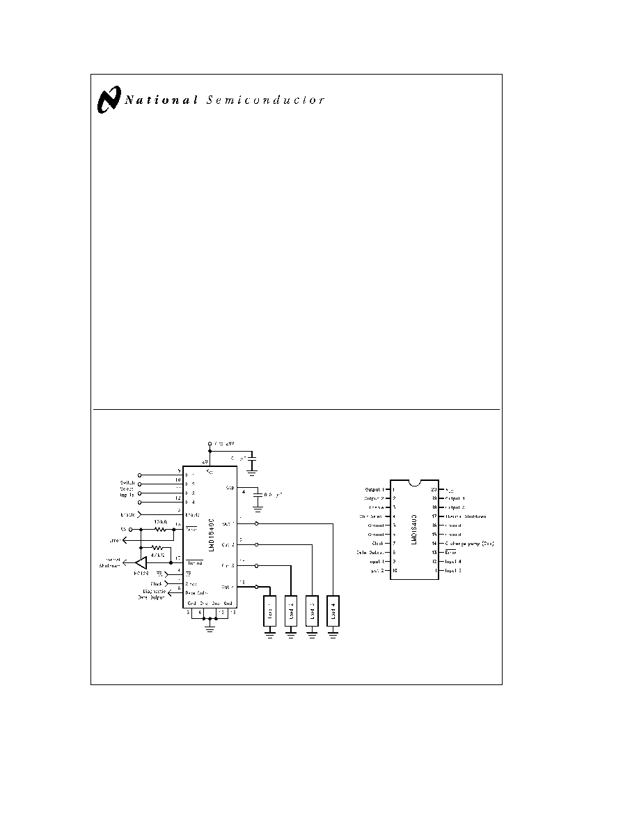
Typical Application
TL H 11026 ≠ 1
Connection Diagram
TL H 11026 ≠ 2
Order Number LMD18400N
See NS Package Number N20A
TRI-STATE
is a registered trademark of National Semiconductor Corporation
MICROWIRE
TM
is a trademark of National Semiconductor Corporation
C1996 National Semiconductor Corporation
RRD-B30M76 Printed in U S A
http
www national com
Absolute Maximum Ratings
(Note 1)
If Military Aerospace specified devices are required
please contact the National Semiconductor Sales
Office Distributors for availability and specifications
Supply Survival Voltage (Pin 20)
Transient (t
e
10 ms)
80V
Continuous
b
0 5V to
a
60V
Output Transient Current (Each Switch)
3 75A
Output Transient Current (Total All Switches)
6A
Output Steady State Current (Each Switch)
1A
Logic Input Voltage (Pins 3 9 10 11 12)
b
0 3V to
a
16V
Logic Input Voltage (Pins 4 7)
b
0 3V to
a
6V
Error Flag Voltage
16V
ESD Susceptibility (Note 2)
2000V
Power Dissipation (Note 3)
5W
Internally Limited
Junction Temperature (T
JMax
)
150 C
Storage Temperature Range
b
65 C to
a
150 C
Lead Temperature (Soldering 10 Sec )
a
260 C
Operating Ratings
(Note 1)
Ambient Temperature Range (T
A
)
b
25 C to
a
85 C
Supply Voltage Range
7V to 28V
Electrical Characteristics
V
CC
e
12V C
CP
e
0 01 mFd unless otherwise indicated Boldface limits apply
over the entire operating temperature range
b
25 C
s
T
A
s
a
85 C all other limits are for T
A
e
T
J
e a
25 C
Parameter
Conditions
Typical
Limit
Units
(Note 4)
(Note 5)
(Limit)
DC CHARACTERISTICS
Supply Current
Enable Input
e
0V
0 04
10
m
A (Max)
Enable Input
e
5V Inputs
e
0V
7 5
15
mA (Max)
Enable Input
e
5V Inputs
e
5V
Open Loads
7 5
15
mA (Max)
Output Leakage
Enable Input
e
0V Inputs
e
0V
0 01
300
m
A (Max)
(Pins 1 2 18 19)
Rds ON
I
OUT
e
1A (Note 6)
0 8
1 3
X
(Max)
Short Circuit Current
V
CC
e
12V (Note 6)
1 2
0 6
A (Min)
V
CC
e
7V (Note 6)
2 4
A
V
CC
e
28V (Note 6)
0 6
A
Maximum Output Current
V
CC
b
V
O
e
4V (Note 6)
3 75
A
Load Error Threshold Voltage
Pins 1 2 18 19
4 1
V
Open Load Detection Current
Pins 1 2 18 19
150
m
A
Negative Clamp Output Voltage
I
O
e
1A (Note 6)
b
5
V
Overvoltage Shutdown Threshold
31
40
V (Max)
Overvoltage Shutdown Hysteresis
0 75
V
Error Output Leakage Current
V
Pin 13
e
12V
0 001
10
m
A (Max)
Thermal Warning Temperature
V
Pin 13
k
0 8V
145
C
Thermal Shutdown Temperature
V
Pin 17
k
0 8V
170
C
http
www national com
2
Electrical Characteristics
V
CC
e
12V C
CP
e
0 01 mF unless otherwise indicated Boldface limits apply
over the entire operating temperature range
b
25 C
s
T
A
s
a
85 C all other limits are for T
A
e
T
J
e a
25 C (Continued)
Parameter
Conditions
Typical
Limit
Units
(Note 4)
(Note 5)
(Limit)
AC CHARACTERISTICS
Switch Turn-On Delay
Enable (Pin 3)
e
5V
5
10
m
s (Max)
(t
d(ON)
)
I
OUT
e
1A
Switch Turn-On Rise
I
OUT
e
1A
7
15
m
s (Max)
Time (t
ON
)
Switch Turn-Off Delay
Enable (Pin 3)
e
5V
0 5
2
m
s (Max)
(t
dOFF
)
I
OUT
e
1A
Switch Turn-Off Fall
I
OUT
e
1A
0 15
1
m
s (Max)
Time (t
OFF
)
Enable Time (t
EN
)
Measured with Switch 1
30
50
m
s (Max)
Pin 9
e
5V
Error Reporting Delay
Enable (Pin 3)
e
5V
75
150
m
s (Max)
(t
Error
)
Switch 1 Load Opened
Data Setup Time (t
DS
)
C
L
e
30 pF
200
500
ns (Min)
TRI-STATE Control (t
1H
t
OH
)
Pin 8 Hi-Z Enable Time
2
m
s
Data Clock Frequency
3
1
MHz (Max)
DIGITAL CHARACTERISTICS
Logic ``1'' Input Voltage
Pins 3 4 7 9 10 11 12
2 0
V (Min)
Logic ``0'' Input Voltage
Pins 3 4 7 9 10 11 12
0 8
V (Max)
Logic ``1'' Input Current
Pins 4 7
0 001
1
m
A (Max)
Logic ``0'' Input Current
Pins 4 7
b
0 001
b
1
m
A (Max)
TRI-STATE Output Current
Pin 8 Pin 4
e
5V
0 05
10
m
A (Max)
Pin 8
e
0V
b
0 05
b
10
m
A (Max)
Enable Input Current
Pin 3
e
2 4V
12
25
m
A (Max)
Channel Input Resistance
Pins 9 10 11 12
75
15
kX (Min)
Error Output Sink Current
Pin 13
e
0 8V
4
1 6
mA (Min)
Logic ``1'' Output Voltage
Pin 8
I
OUT
e b
360 mA
4 4
2 4
V (Min)
I
OUT
e b
10 mA
5 1
4 5
V (Min)
I
OUT
e b
10 mA
5 5
V (Max)
Logic ``0'' Output Voltage
Pin 8
0 4
V (Max)
I
OUT
e
100 mA
Thermal Shutdown Output
Pin 17
e
2 4V
5
3
m
A (Min)
Source Current
Thermal Shutdown Output
Pin 17
e
0 8V
360
250
m
A (Min)
Sink Current
http
www national com
3
Electrical Characteristics Notes
Note 1
Absolute Maximum Ratings indicate limits beyond which damage to the device may occur Operating Ratings indicate conditions for which the device is
intended to be functional but do not guarantee specific performance limits For guaranteed specifications and test conditions see the Electrical Characteristics
Note 2
Human body model 100 pF discharge through a 1 5 kX resistor All pins except pins 8 and 13 which are protected to 1000V and pins 1 2 18 and 19 which
are protected to 500V
Note 3
The maximum power dissipation is a function of T
JMax
i
JA
and T
A
and is limited by thermal shutdown The maximum allowable power dissipation at any
ambient temperature is P
D
e
(T
JMax
b
T
A
) i
JA
If this dissipation is exceeded the die temperature will rise above 150 C and the device will eventually go into
thermal shutdown For the LMD18400 the junction-to-ambient thermal resistance i
JA
is 60 C W With sufficient heatsinking the maximum continuous power
dissipation for the package will be I
DCMax
2 c
R
ON(Max)
c
4 switches (1A
2 c
1 3X
c
4
e
5 2W)
Note 4
Typical values are at T
J
e a
25 C and represent the most likely parametric norm
Note 5
All limits are 100% production tested at
a
25 C Limits at temperature extremes are guaranteed through correlation and accepted Statistical Quality
Control (SQC) methods
Note 6
Pulse Testing techniques used Pulse width is
k
5 ms with a duty cycle
k
1 %
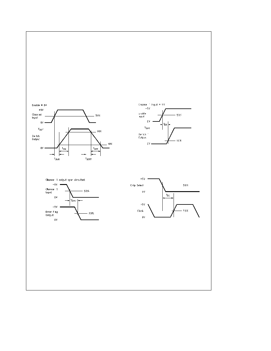
Timing Specification Definitions
Switching Turn ON OFF
TL H 11026 ≠ 3
Enable Turn-ON
TL H 11026 ≠ 4
Error Reporting Delay
TL H 11026 ≠ 5
Data Setup Time
TL H 11026 ≠ 6
http
www national com
4
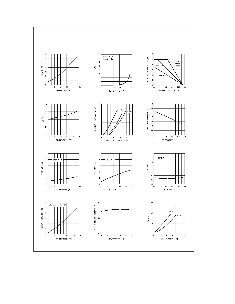
Typical Performance Characteristics
For all curves V
CC
e
12V Temperature is the junction temperature unless otherwise noted
vs Temperature
Switch ON Resistance
TL H 11026 ≠ 31
vs Temperature
``Sleep'' Mode Supply Current
TL H 11026 ≠ 32
Ambient Temperature
Dissipation vs
Maximum Power
TL H 11026 ≠ 33
vs Temperature
Short Circuit Current
TL H 11026 ≠ 34
vs Temperature
Clamp Characteristics
TL H 11026 ≠ 35
Voltage vs Temperature
Error Sense Threshold
TL H 11026 ≠ 36
vs Temperature
Turn ON Rise Time
TL H 11026 ≠ 37
vs Temperature
Turn ON Delay Time
TL H 11026 ≠ 38
vs Temperature
Turn OFF Time
TL H 11026 ≠ 39
Resistance vs Temperature
Switch Select Logic Input
TL H 11026 ≠ 40
vs Temperature
Enable Threshold Voltage
TL H 11026 ≠ 41
vs Sink Current
Error Output Voltage
TL H 11026 ≠ 42
http
www national com
5