ChipFind - документация

Электронный компонент: LMF90CC

Скачать:  PDF   ZIP
TL H 10354
LMF90
4th-Order
Elliptic
Notch
Filter
December 1994
LMF90
4th-Order Elliptic Notch Filter
General Description
The LMF90 is a fourth-order elliptic notch (band-reject) filter
based on switched-capacitor techniques No external com-
ponents are needed to define the response function The
depth of the notch is set using a two-level logic input and
the width is programmed using a three-level logic input Two
different notch depths and three different ratios of notch
width to center frequency may be programmed by connect-
ing these pins to V
a
ground or V
b
Another three-level
logic pin sets the ratio of clock frequency to notch frequen-
cy
An internal crystal oscillator is provided Used in conjunction
with a low-cost color TV crystal and the internal clock fre-
quency divider a notch filter can be built with center fre-
quency at 50 Hz 60 Hz 100 Hz 120 Hz 150 Hz or 180 Hz
for rejection of power line interference Several LMF90s can
be operated from a single crystal An additional input is pro-
vided for an externally-generated clock signal
Features
Y
Center frequency set by external clock or on-board
clock oscillator
Y
No external components needed to set response char-
acteristics
Y
Notch width attenuation and clock-to-center-frequency
ratio independently programmable
Y
14 pin 0 3
wide package
Key Specifications
Y
f
0
Range
0 1 Hz to 30 kHz
Y
f
0
accuracy over full temperature range (max)
1 5%
Y
Supply voltage range
g
2V to
g
7 5V or 4V to 15V
Y
Passband Ripple (typ)
0 25 dB
Y
Attenuation at f
0
(typ)
39 dB or 48 dB (selectable)
Y
f
CLK
f
0
100 1 50 1 or 33 3 1
Y
Notch Bandwidth (typ)
0 127 f
0
0 26 f
0
or 0 55 f
0
Y
Output offset voltage (max)
120 mV
Applications
Y
Automatic test equipment
Y
Communications
Y
Power line interference rejection
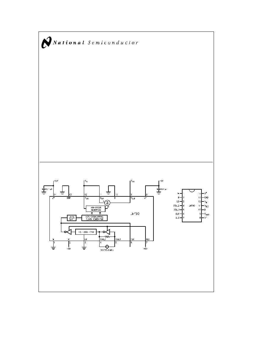
Typical Connection
60 Hz Notch Filter
TL H 10354 1
Connection
Diagram
Dual-In-Line and Small
Outline Packages
TL H 10354 2
Top View
Order Number LMF90CCN
LMF90CIWM
LMF90CCWM LMF90CIJ
LMF90CCJ LMF90CIN
LMF90CMJ or
LMF90CMJ 883
See NS Package Number
J14A M14B or N14A
C1995 National Semiconductor Corporation
RRD-B30M115 Printed in U S A
Absolute
Maximum
Ratings
(Note
s13
)
If
MilitaryAerospace
specified
devices
are
required
Soldering
Information
(Note
4)
please
contact
the
National
Semiconductor
Sales
N
Package
(Soldering
10
sec)
260
C
OfficeDistributors
for
availability
and
specifications
J
Package
(Soldering
10
sec)
300
C
Supply
Voltage
(V
S
e
V
a
b
V
b
)
b
03V
to
a
16V
Storage
Temperature
Range
b
65
Ct
o
a
150
C
Voltage
at
any
Input
or
Output
V
b
b
03V
to
V
a
a
03V
Junction
Temperature
150
C
Input
Current
at
any
Pin
(Note
10)
5
m
A
Operating
Ratings
(Note
s23
)
Package
Input
Current
(Note
10)
20
mA
Temperature
Range
T
MIN
s
T
A
s
T
MAX
Power
Dissipation
(Note
5)
500
mW
LMF90CCN
LMF90CCWM
ESD
Susceptability
(Note
6)
LMF90CCJ
0
C
s
T
A
s
a
70
C
Pin
9
1800V
LMF90CIJ
LMF90CIWM
LMF90CIN
All
Other
Pins
2000V
b
40
C
s
T
A
s
a
85
C
LMF90CMJ
LMF90CMJ883
b
55
C
s
T
A
s
a
125
C
Supply
Voltage
Range
40V
to
150V
AC
Electrical
Characteristics
The
following
specifications
apply
for
V
a
ea
5V
and
V
b
eb
5V
unless
otherwise
specified
Boldface
limits
apply
for
T
A
e
T
MIN
to
T
MAX
all
other
limits
T
A
e
T
J
e
25
C
LMF90CCJ
LMF90CCN
LMF90CIJ
LMF90CIWM
LMF90CCWM
LMF90CIN
LMF90CMJ
Units
Symbol
Parameter
Conditions
Typ
Tested
Design
Typ
Tested
Design
(Limit)
(Note
7)
Limit
Limit
(Note
7)
Limit
Limit
(Note
8)
(Note
9)
(Note
8)
(Note
9)
f
O
Center
Frequency
01
01
Hz
(Min)
Range
30
30
30
kHz
(Max)
f
CLK
Clock
Frequency
Pin
6
1
0
1
0
H
z
(Min)
Range
Pin
6
15
15
15
MHz
(Max)
Pins
4
and
5
40
40
40
MHz
(Max)
f
CLK
f
O1
Clock-to-Center-
W
e
D
e
V
b
R
e
V
a
335
g
1%
335
g
15%
335
g
15%
(Max)
Frequency
Ratio
f
CLK
e
167
kHz
f
CLK
f
O2
W
e
D
e
R
e
GND
5025
g
1%
5025
g
15%
5025
g
15%
(Max)
f
CLK
e
250
kHz
f
CLK
f
O3
W
e
V
a
D
e
GND
R
e
V
b
1005
g
1%
1005
g
15%
1005
g
15%
(Max)
f
CLK
e
500
kHz
H
ON
Passband
Gain
DC
and
20
kHz
W
e
D
e
V
b
R
e
V
a
0
g
02
g
02
0
g
02
dB
(Max)
f
CLK
e
167
kHz
W
e
D
e
R
e
GND
0
g
02
g
02
0
g
02
dB
(Max)
f
CLK
e
250
kHz
W
e
V
a
D
e
GND
R
e
V
b
0
g
02
g
02
0
g
02
dB
(Max)
f
CLK
e
500
kHz
2
AC
Electrical
Characteristics
The
following
specifications
apply
for
V
a
ea
5V
and
V
b
eb
5V
unless
otherwise
specified
Boldface
limits
apply
for
T
A
e
T
MIN
to
T
MAX
all
other
limits
T
A
e
T
J
e
25
C
(Continued)
LMF90CCJ
LMF90CCN
LMF90CIJ
LMF90CIWM
LMF90CCWM
LMF90CIN
LMF90CMJ
Units
Symbol
Parameter
Conditions
Typ
Tested
Design
Typ
Tested
Design
(Limit)
(Note
7)
Limit
Limit
(Note
7)
Limit
Limit
(Note
8)
(Note
9)
(Note
8)
(Note
9)
PBW
Ratio
of
Passband
W
e
D
e
V
b
R
e
V
a
01275
g
00175
01275
g
00175
01275
g
00175
(Max)
Width
to
Center
f
CLK
e
167
kHz
Frequency
W
e
D
e
R
e
GND
0265
g
0025
0265
g
0025
0265
g
0025
(Max)
f
CLK
e
250
kHz
W
e
V
a
D
e
GND
R
e
V
b
0550
g
005
0550
g
005
0550
g
005
(Max)
f
CLK
e
500
kHz
A
Min1
f
O1
Gain
at
W
e
D
e
V
b
R
e
V
a
b
39
b
30
b
30
b
39
b
30
dB
(Max)
Center
Frequency
f
CLK
e
167
kHz
A
Min2
f
O2
W
e
D
e
R
e
GND
b
48
b
365
b
365
b
48
b
365
dB
(Max)
f
CLK
e
250
kHz
A
Min3
f
O3
W
e
V
a
D
e
GND
R
e
V
b
b
48
b
365
b
365
b
48
b
365
dB
(Max)
f
CLK
e
500
kHz
Additional
Center
W
e
GND
D
e
V
b
R
e
V
a
b
36
b
30
b
30
b
36
b
30
dB
(Max)
Frequency
Gain
f
CLK
e
167
kHz
Tests
at
f
O1
W
e
V
a
D
e
V
b
R
e
V
a
b
36
b
30
b
30
b
36
b
30
dB
(Max)
f
CLK
e
167
kHz
W
e
V
b
D
e
GND
R
e
V
a
b
42
b
30
b
30
b
42
b
30
dB
(Max)
f
CLK
e
167
kHz
W
e
D
e
GND
R
e
V
a
b
48
b
35
b
35
b
48
b
35
dB
(Max)
f
CLK
e
167
kHz
W
e
V
a
D
e
GNDR
e
V
a
b
48
b
35
b
35
b
48
b
35
dB
(Max)
f
CLK
e
167
kHz
3
AC
Electrical
Characteristics
The
following
specifications
apply
for
V
a
ea
5V
and
V
b
eb
5V
unless
otherwise
specified
Boldface
limits
apply
for
T
A
e
T
MIN
to
T
MAX
all
other
limits
T
A
e
T
J
e
25
C
(Continued)
LMF90CCJ
LMF90CCN
LMF90CIJ
LMF90CIWM
LMF90CCWM
LMF90CIN
LMF90CMJ
Units
Symbol
Parameter
Conditions
Typ
Tested
Design
Typ
Tested
Design
(Limit)
(Note
7)
Limit
Limit
(Note
7)
Limit
Limit
(Note
8)
(Note
9)
(Note
8)
(Note
9)
Additional
Center
W
e
V
b
D
e
V
b
R
e
GND
b
36
b
30
b
30
b
36
b
30
dB
(Max)
Frequency
Gain
f
CLK
e
250
kHz
Tests
at
f
O2
W
e
GND
D
e
V
b
R
e
GND
b
36
b
30
b
30
b
36
b
30
dB
(Max)
f
CLK
e
250
kHz
W
e
V
a
D
e
V
b
R
e
GND
b
36
b
30
b
30
b
36
b
30
dB
(Max)
f
CLK
e
250
kHz
W
e
V
b
D
e
R
e
GND
b
42
b
30
b
30
b
42
b
30
dB
(Max)
f
CLK
e
250
kHz
W
e
V
a
D
e
R
e
GND
b
48
b
35
b
35
b
48
b
35
dB
(Max)
f
CLK
e
250
kHz
Additional
Center
W
e
D
e
R
e
V
b
b
36
b
30
b
30
b
36
b
30
dB
(Max)
Frequency
Gain
f
CLK
e
500
kHz
Tests
at
f
O3
W
e
GND
D
e
V
b
R
e
V
b
b
36
b
30
b
30
b
36
b
30
dB
(Max)
f
CLK
e
500
kHz
W
e
V
a
D
e
V
b
R
e
V
b
b
36
b
30
b
30
b
36
b
30
dB
(Max)
f
CLK
e
500
kHz
W
e
V
b
D
e
GND
R
e
V
b
b
42
b
30
b
30
b
42
b
30
dB
(Max)
f
CLK
e
500
kHz
W
e
D
e
GND
R
e
V
b
b
48
b
35
b
35
b
48
b
35
dB
(Max)
f
CLK
e
500
kHz
A
3a
Gain
at
f
3
e
0995
f
O1
W
e
D
e
V
b
R
e
V
a
b
41
b
30
b
30
b
41
b
30
dB
(Max)
A
4a
Gain
at
f
4
e
1005
f
O1
f
CLK
e
167
kHz
b
41
b
30
b
30
b
41
b
30
dB
(Max)
A
3b
Gain
at
f
3
e
0992
f
O2
W
e
D
e
R
e
GND
f
CLK
e
250
kHz
b
40
b
35
b
35
b
40
b
35
dB
(Max)
A
4b
Gain
at
f
4
e
1008
f
O2
b
40
b
35
b
35
b
40
b
35
dB
(Max)
A
3c
Gain
at
f
3
e
0982
f
O3
W
e
V
a
D
e
GND
R
e
V
b
b
41
b
35
b
35
b
41
b
35
dB
(Max)
A
4c
Gain
at
f
4
e
1018
f
O3
f
CLK
e
500
kHz
b
41
b
35
b
35
b
41
b
35
dB
(Max)
A
max1
Passband
Ripple
W
e
D
e
V
b
R
e
V
a
f
5
e
0914
f
O1
025
09
09
025
09
dB
(Max)
f
CLK
e
167
kHz
025
0
0
025
0
dB
(Min)
f
6
e
1094
f
O1
025
09
09
025
09
dB
(Max)
025
0
0
025
0
dB
(Min)
4
AC
Electrical
Characteristics
The
following
specifications
apply
for
V
a
ea
5V
and
V
b
eb
5V
unless
otherwise
specified
Boldface
limits
apply
for
T
A
e
T
MIN
to
T
MAX
all
other
limits
T
A
e
T
J
e
25
C
(Continued)
LMF90CCJ
LMF90CCN
LMF90CIJ
LMF90CIWM
LMF90CCWM
LMF90CIN
LMF90CMJ
Units
Symbol
Parameter
Conditions
Typ
Tested
Design
Typ
Tested
Design
(Limit)
(Note
7)
Limit
Limit
(Note
7)
Limit
Limit
(Note
8)
(Note
9)
(Note
8)
(Note
9)
A
Max2
Passband
Ripple
W
e
D
e
R
e
GND
f
5
e
0830
f
O2
025
09
09
026
09
dB
(Max)
f
CLK
e
250
kHz
025
0
0
025
0
dB
(Min)
f
6
e
1205
f
O2
025
09
09
025
09
dB
(Max)
025
0
0
025
0
dB
(Min)
A
Max3
Passband
Ripple
W
e
V
a
D
e
GND
R
e
V
b
f
5
e
0700
f
O3
025
09
09
025
09
dB
(Max)
f
CLK
e
500
kHz
025
0
0
025
0
dB
(Min)
f
6
e
1428
f
O3
025
09
09
025
09
dB
(Max)
025
0
0
025
0
dB
(Min)
E
n
Output
Noise
20
kHz
Bandwidth
W
e
D
e
V
b
R
e
V
a
f
CLK
e
167
kHz
670
670
m
Vrms
W
e
D
e
R
e
GND
f
CLK
e
250
kHz
370
370
m
Vrms
W
e
V
a
D
e
GND
R
e
V
b
250
250
m
Vrms
f
CLK
e
500
kHz
Clock
Feedthrough
50
50
mVp
p
GBW
Output
Buffer
1
1
MHz
Gain
Bandwidth
SR
Output
Buffer
33
V
m
s
Slew
Rate
C
L
Maximum
Capacitive
200
200
pF
Load
5