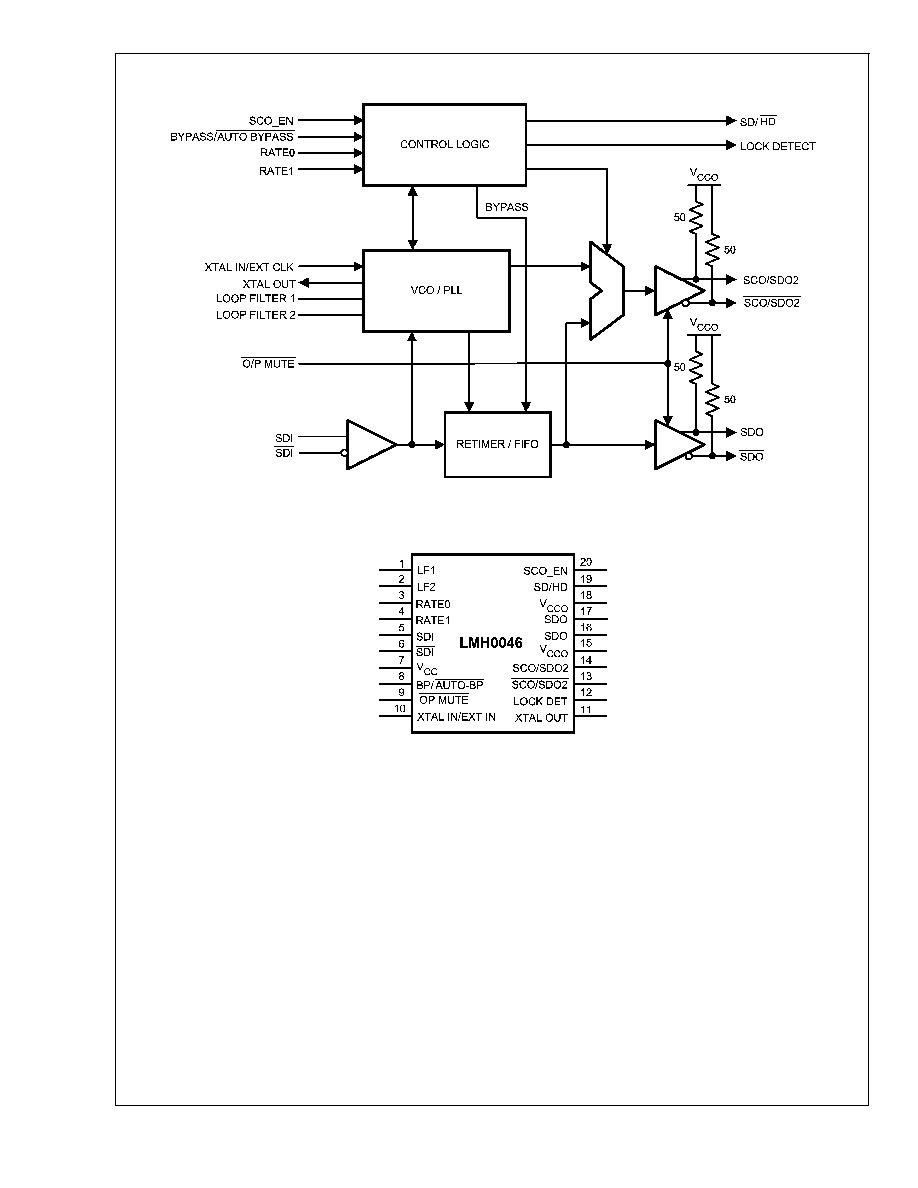
LMH0046
HD/SD Multi-Rate Serial Digital Video Data Reclocker
General Description
The LMH0046 HD/SD Multi-Rate Serial Digital Video Data
Reclocker is a monolithic integrated circuit that retimes bit-
serial digital video data conforming to the SMPTE 259M (A &
C) and SMPTE 292M standards. The LMH0046 operates at
serial data rates of 143 Mbps, 270 Mbps, 1.483 Gbps and
1.485 Gbps. The LMH0046 supports DVB-ASI operation at
270 Mbps.
The LMH0046 automatically detects the incoming data rate
and adjusts itself to retime the incoming data to suppress
accumulated jitter. The LMH0046 recovers the serial data-
rate clock and optionally provides it as an output. The
LMH0046 has two differential serial data outputs; the second
output may be selected as a low-jitter, data-rate clock output.
Controls and indicators are: serial clock or second serial
data output select, manual rate select input, SD/HD rate
indicator output, lock detect output, auto/manual data by-
pass and output mute. The serial data inputs, outputs, and
serial data-rate clock outputs are differential LVPECL com-
patible. The CML serial data and serial data-rate clock out-
puts are suitable for driving 100
differentially terminated
networks. The control logic inputs and outputs are LVCMOS
compatible.
The LMH0046 is powered from a single 3.3V supply. Power
dissipation is typically 330 mW. The device is housed in a
20-pin TSSOP package.
Features
n
Supports SMPTE 259M (A & C) and SMPTE 292M
serial digital video standards
n
Supports 143 Mbps, 270 Mbps, 1.483 Gbps, and 1.485
Gbps serial data rate operation
n
Supports DVB-ASI at 270 Mbps
n
Single 3.3V supply operation
n
330 mW typical power consumption
n
Two differential, reclocked outputs
n
Choice of second reclocked output or low-jitter,
differential, data-rate clock output
n
Single 27 MHz external crystal or reference clock input
n
Manual rate select input
n
SD/HD operating rate indicator output
n
Lock Detect indicator output
n
Output mute function for data and clock
n
Auto/Manual reclocker bypass
n
Differential LVPECL compatible serial data inputs and
outputs
n
LVCMOS control inputs and indicator outputs
n
20-Pin TSSOP package
n
Industrial temperature range: -40∞C to +85∞C
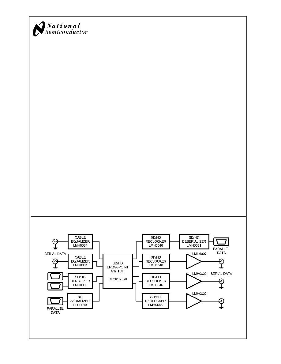
Applications
n
SDTV/HDTV serial digital video interfaces for:
-- Digital video routers and switchers
-- Digital video processing and editing equipment
-- DVB-ASI equipment
-- Video standards and format converters
Typical Application
20182601
PRELIMINARY
April 2006
LMH0046
HD/SD
Multi-Rate
Serial
Digital
V
ideo
Data
Reclocker
© 2006 National Semiconductor Corporation
DS201826
www.national.com

Pin Descriptions
TSSOP Pin
Name
Description
1
LF1
Loop Filter
2
LF2
Loop Filter
3
RATE 0
Data Rate Select Input
4
RATE 1
Data Rate Select Input
5
SDI
Data Input True
6
SDI
Data Input Complement
7
V
CC
Positive power supply input
8
BYPASS/AUTO BYPASS
Bypass/Auto Bypass mode select
9
OUTPUT MUTE
Data and Clock Output Mute Input (active LOW)
10
XTAL IN/EXT CLK
Crystal or External Oscillator Input
11
XTAL OUT
Crystal Oscillator Output
12
LOCK DETECT
PLL Lock Detect Output (active HIGH)
13
SCO/SDO2
Serial Clock or Serial Data Output 2 Complement
14
SCO/SDO2
Serial Clock or Serial Data Output 2 True
15
V
CCO
Positive power supply input (Output Driver)
16
SDO
Data Output Complement
17
SDO
Data Output True
18
V
CCO
Positive power supply input (Output Driver)
19
SD/HD
Data Rate Range Output
20
SCO_EN
Multiplexer control, Serial Clock or Serial Data 2 Output
LMH0046
www.national.com
3
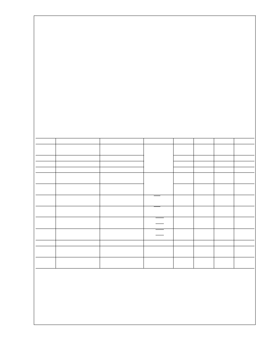
Absolute Maximum Ratings
(Note 1) It
is anticipated that this device will not be offered in a
military qualified version. If Military/Aerospace specified
devices are required, please contact the National Semicon-
ductor Sales Office/Distributors for availability and specifi-
cations.
Supply Voltage (V
CC
≠V
EE
)
4.0V
Logic Supply Voltage (Vi)
V
EE
-0.15V to
V
CC
+0.15V
Logic Input Current (single input):
Vi = V
EE
-0.15V
-5 mA
Vi = V
CC
+0.15V
+5 mA
Logic Output Voltage (Vo)
V
EE
-0.15V to
V
CC
+0.15V
Logic Output Source/Sink Current
±
8 mA
Serial Data Input Voltage (V
SDI
)
V
CC
to V
CC
-2.0V
Serial Data Output Sink Current (I
SDO
)
24 mA
Package Thermal Resistance, TSSOP
JA
36∞C/W
JC
6.4∞C/W
Storage Temp. Range
-65∞C to +150∞C
Junction Temperature
+150∞C
Lead Temperature (Soldering 4 Sec)
+260∞C (Pb-free)
ESD Rating (HBM)
2 kV
ESD Rating (MM)
250V
Recommended Operating
Conditions
Supply Voltage (V
CC
≠V
EE
)
3.3V
±
5%
Logic Input Voltage
V
EE
to V
CC
Differential Serial Input Voltage
800 mV
±
10%
Serial Data or Clock Output Sink
Current (I
SO
)
16 mA max.
Operating Free Air Temperature (T
A
)
-40∞C to +85∞C
DC Electrical Characteristics
Over Supply Voltage and Operating Temperature ranges, unless otherwise specified. (Notes 2, 3)
Symbol
Parameter
Conditions
Reference
Min
Typ
Max
Units
V
IH
Input Voltage High
Level
Logic level
inputs
2
V
CC
V
V
IL
Input Voltage Low Level
V
EE
0.8
V
I
IH
Input Current High Level V
IH
= V
CC
1
20
µA
I
IL
Input Current Low Level
V
IL
= V
EE
-1
-20
µA
V
OH
Output Voltage High
Level
I
OH
= -2 mA
All logic level
outputs
2
V
V
OL
Output Voltage Low
Level
I
OL
= +2 mA
V
EE
+ 0.6
V
V
SDID
Serial Input Voltage,
Differential
SDI, SDI
200
1600
mV
P-P
V
CMI
Input Common Mode
Voltage
SDI, SDI
V
CC
-1.6
V
CC
-0.2
V
V
SDOD
Serial Output Voltage,
Differential
100
differential load
SCO, SCO
720
800
880
mV
P-P
SDO, SDO
V
CMO
Output Common Mode
Voltage
100
differential load
SCO, SCO
V
CC
-
V
SDO, SDO
V
SDOD
/2
I
LEAK
Leakage Current
LF1, LF2
TBD
µA
I
CC
Power Supply Current,
3.3V supply, Total
270 Mbps, NTSC color
bar pattern
100
mA
I
CC
Power Supply Current,
3.3V supply, Total
1485 Mbps, NTSC color
bar pattern
100
mA
LMH0046
www.national.com
4
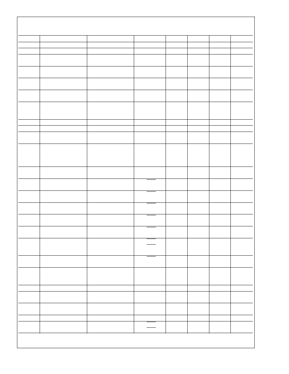
AC Electrical Characteristics
Over Supply Voltage and Operating Temperature ranges, unless otherwise specified. (Note 3)
Symbol
Parameter
Conditions
Reference
Min
Typ
Max
Units
BR
SD
Serial Data Rate
SMPTE 259M, A
SDI, SDO
143
Mbps
BR
SD
Serial Data Rate
SMPTE 259M, C
SDI, SDO
270
Mbps
BR
SD
Serial Data Rate
SMPTE 292M
SDI, SDO
1483,
1485
Mbps
TOL
JIT
Serial Input Jitter
Tolerance
143 or 270 Mbps,
(Notes 7, 8, 9)
SDI
>
6
UI
P-P
TOL
JIT
Serial Input Jitter
Tolerance
143 or 270 Mbps,
(Notes 7, 8, 10, 13)
SDI
>
0.6
UI
P-P
TOL
JIT
Serial Input Jitter
Tolerance
1483 Mbps or 1485
Mbps, (Notes 7, 8, 9)
SDI
>
6
UI
P-P
TOL
JIT
Serial Input Jitter
Tolerance
1483 Mbps or 1485
Mbps, (Notes 7, 8, 10,
13)
SDI
>
0.6
UI
P-P
t
JIT
Additive Output Jitter
143 Mbps, (Note 8)
SDO
0.02
0.08
UI
P-P
t
JIT
Additive Output Jitter
270 Mbps, (Note 8)
SDO
0.02
0.08
UI
P-P
t
JIT
Additive Output Jitter
1483 Mbps, 1485 Mbps,
(Note 8)
SDO
0.05
0.1
UI
P-P
BW
Jitter Transfer Function
-3 dB Bandwidth
(Fractional Loop
Bandwidth)
All supported data rates,
(Note 11)
0.1
0.25
0.35
%BR
SD
Jitter Transfer Function
Peaking
All supported data rates,
(Note 12)
0.05
0.1
dB
F
CO
Serial Clock Output
Frequency
143 Mbps data rate
SCO, SCO
143
MHz
F
CO
Serial Clock Output
Frequency
270 Mbps data rate
SCO, SCO
270
MHz
F
CO
Serial Clock Output
Frequency
1483 Mbps data rate
SCO, SCO
1483
MHz
F
CO
Serial Clock Output
Frequency
1485 Mbps data rate
SCO, SCO
1485
MHz
t
JIT
Serial Clock Output
Jitter
SCO, SCO
2
3
ps
RMS
Serial Clock Output
Alignment with respect
to Data Interval
SDO, SDO,
SCO, SCO
35
65
%
Serial Clock Output
Duty Cycle
SCO, SCO
40
60
%
T
ACQ
Acquisition Time
Color bar pattern or
PRBS 23 sequence.
(Note 6)
10
ms
t
r
, t
f
Input rise/fall time
10%≠90%
Logic inputs
1.5
3
ns
t
r
, t
f
Input rise/fall time
20%≠80%, 143 or 270
Mbps
SDI
400
1500
ps
t
r
, t
f
Input rise/fall time
20%≠80%, 1483 or
1485 Mbps
SDI
80
120
170
ps
t
r
, t
f
Output rise/fall time
10%≠90%, C
L
= 5 pF
Logic outputs
1.5
3
ns
t
r
, t
f
Output rise/fall time
20%≠80%,1483 or 1485
Mbps, (Note 5)
SDO, SDO,
SCO, SCO
90
130
ps
LMH0046
www.national.com
5