 | –≠–ª–µ–∫—Ç—Ä–æ–Ω–Ω—ã–π –∫–æ–º–ø–æ–Ω–µ–Ω—Ç: LMH1251 | –°–∫–∞—á–∞—Ç—å:  PDF PDF  ZIP ZIP |
LMH1251
YP
B
P
R
to RGB Decoder and 2:1 Video Switch
General Description
The LMH
TM
1251 is a wideband 2:1 analog video switch with
an integrated YP
B
P
R
to RGB decoder. The device accepts
one set of YP
B
P
R
inputs and one set of RGB/HSYNC/
VSYNC inputs. Based on the input selected, the output will
be either a decoded TV or buffered PC video signal.
The LMH1251 has a SYNC separator and processor that is
capable of extracting sync timing information from both Stan-
dard Definition Television (SDTV) and High Definition Tele-
vision (HDTV) inputs. It provides bi-level sync, and tri-level
sync separation.
The color space conversion from YP
B
P
R
to RGB in the
LMH1251 is realized with a very high precision fully analog
dematrixer that provides chrominance accuracy that is less
than 2.5% of amplitude & 1.5∞ of phase error on a vector-
scope. It is equipped with a smart video detection circuit
which automatically senses SDTV and HDTV video formats
and applies the appropriate color space conversion.
The LMH1251 is capable of handling SDTV, HDTV, XGA,
SXGA, and UXGA video formats, which makes it an ideal
solution for enhancing value in applications ranging from
LCD monitors, to set-top boxes, to projectors. The LMH1251
is available in a TSSOP-24 package.
Features
n
YP
B
P
R
to RGB decoding
n
YP
B
P
R
path: 70 MHz, -3 dB, 700 mV
PP
bandwidth
n
RGB path: 400 MHz, -3 dB, 700 mV
PP
bandwidth
n
Supports PC video display resolutions up to UXGA
(1600 x 1200
@
75 Hz)
n
Supports 480i, 480p, 576i, 576p, 720p, 1080i, and
1080p
n
Smart video format detection for SD and HD
n
Power save mode
Applications
n
TFT LCD monitor
n
CRT monitor
n
Set-top box
n
Display projector
Connection Diagram
24-Pin TSSOP
20151927
Top View
LMH
TM
is a trademark of National Semiconductor Corporation.
August 2005
LMH1251
YP
B
P
R
to
RGB
Decoder
and
2:1
V
ideo
Switch
© 2005 National Semiconductor Corporation
DS201519
www.national.com
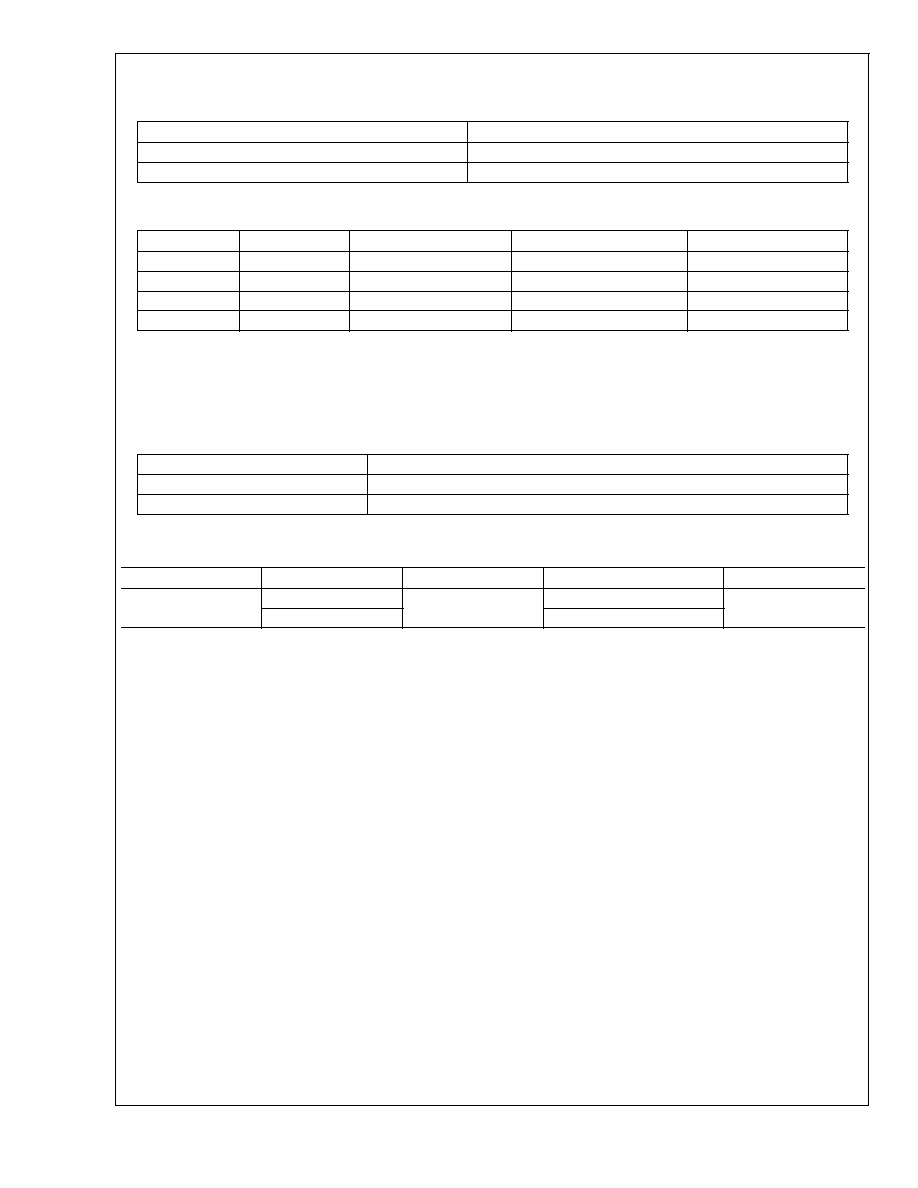
Truth Table
TABLE 1. Input Select
Pin 24
OUT
0
RGBhv input Ch
1
YP
B
P
R
input Ch
TABLE 2.
Pin 23
Pin 22
SYNC
Format Detection
Decoding Scheme
0
0
Bi-Level
Manual
480p
0
1
Tri-Level
Manual
720p/180i
1
*Outputs 0
Bi-Level
Auto
480p
1
*Outputs 1
Tri-Level
Auto
720p/1080i
Note: * When Pin 23 is set high, the LMH1251 is in Auto Mode, in which it can
detect the incoming video format (SD or HD) and apply the appropriate
color decoding and sync processing. With Auto Mode, Pin 22 becomes
an output pin, and will either output a logic high or low to notify the user
of the format that is being detected by the LMH1251. If Pin 23 is set
low, the LMH1251 is in Manual Mode, in which the user must specify
the format with Pin 22. With Manual Mode, Pin 22 is an input pin. Since
Pin 22 is a bi-directional pin, care must be taken to not apply any
voltages to it when it is in the Auto Mode, in which it functions as an
output pin. The use of the Auto Mode with Pin 22 left floating is typically
recommended.
TABLE 3. Power Save
Pin 21
Low Power Mode
0
Disable
1
Enabled
Ordering Information
Package
Part Number
Package Marking
Transport Media
NSC Drawing
24-Pin TSSOP
LMH1251MT
LMH1251MT
61 Units/Rail
MTC24
LMH1251MTX
2.5k Units Tape and Reel
LMH1251
www.national.com
2
Absolute Maximum Ratings
(Notes 1, 3)
If Military/Aerospace specified devices are required,
please contact the National Semiconductor Sales Office/
Distributors for availability and specifications.
ESD Tolerance
Susceptibility(Note 4)
4.0 kV
Machine Model (Note 11)
400V
Supply Voltage V
CC
, Pins 7
and 17
5.5V
Voltage at any Input Pin (V
IN
)
V
CC
-0.5
V
IN
0V
Video Inputs (pk-pk)
0.0V
V
IN
1.2V
Thermal Resistance to Ambient
(
JA
)
110∞C/W
Thermal Resistance to Case
(
JC
)
25∞C/W
Junction Temperature (T
J
)
+150∞C
Storage Temperature Range
-65∞C to +150∞C
Lead Temperature (soldering 10
sec.)
265∞C
Operating Ratings
(Note 2)
Operating Temperature Range
0∞C to +70∞C
Supply Voltage (V
CC
)
4.75V
V
CC
5.25V
RGB Video Inputs (pk-pk)
0.0V
V
IN
0.7V
Y Video Inputs (incl. Sync)
-0.3V
V
IN
0.7V
P
B
P
R
Video Inputs
-0.35V
V
IN
0.35V
Video Signal Electrical Characteristics
Unless otherwise noted: T
A
= 25∞C, V
CC
= +5.0V, RGB Video
IN
= 0.70, Y Video
IN
= 0.7 V
PP
, P
B
P
R
Video
IN
=
±
350 VmV,
C
L
= 8 pF, Video Outputs = 0.7 V
PP
. See (Note 7) for Min and Max parameters and (Note 6) for typicals.
Symbol
Parameter
Conditions (Note 2)
Min
Typ
Max
Units
I
S, RGB
Supply Current
No Output Loading, 80 kHz
28
34
41
mA
I
S
, YP
B
P
R
Supply Current
No Output Loading, 480p
see (Note 8)
60
70
80
mA
I
S-PS
Supply Current, Power Save
Mode
Power Save Mode, No Output
Loading, 80 kHz, see (Note 8)
4
8
12
mA
I
OUT
Output Current
3
mA
V
O BLK
Typical DC Active Video Black
Level Output Voltage
No AC Input Signal
1.8
2.1
2.4
VDC
Gain
RGB
RGB Video Unity Gain
RGB Video
IN
= 0.7 V
PP
0.07
dB
Ch-Ch
Match
RGB
RGB Ch to Ch Matching
RGB Video
IN
= 0.7 V
PP
0.02
dB
LE
RGB
RGB Input: Linearity Error
Staircase Input Signal
see (Note 9)
0
%
Video Time Domain Response
RGB t
r
RGB Input:
Video Rise Time
10% to 90%, AC Input Signal
(Note 5)
1.55
ns
RGB OS
R
RGB Input:
Rising Edge Overshoot
AC Input Signal
(Note 5)
3
%
RGB t
f
RGB Input:
Video Fall Time
90% to 10%, AC Input Signal
(Note 5)
1.55
ns
RGB OS
F
RGB Input:
Rising Edge Overshoot
AC Input Signal
(Note 5)
3
%
SD YP
B
P
R
t
r
SD YP
B
P
R
Input:
Video Rise Time
10% to 90%, AC Input Signal
(Note 5)
1.54
ns
RGB OSF
RGB Input:
Falling Edge Overshoot
(Note 5), AC Input Signal
3
%
SD YP
B
P
R
t
r
SD YP
B
P
R
Input:
Video Rise Time
10% to 90%, AC Input Signal
(Note 5)
15.4
ns
SD YP
B
P
R
OS
R
SD YP
B
P
R
Input:
Rising Edge Overshoot
AC Input Signal
(Note 5)
3
%
SD YP
B
P
R
t
f
SD YP
B
P
R
:
Video Fall Time
90% to 10%, AC Input Signal
(Note 5)
15.4
ns
SD YP
B
P
R
OS
F
SD YP
B
P
R
:
Falling Edge Overshoot
AC Input Signal
(Note 5)
3
%
LMH1251
www.national.com
3
Video Signal Electrical Characteristics
(Continued)
Unless otherwise noted: T
A
= 25∞C, V
CC
= +5.0V, RGB Video
IN
= 0.70, Y Video
IN
= 0.7 V
PP
, P
B
P
R
Video
IN
=
±
350 VmV,
C
L
= 8 pF, Video Outputs = 0.7 V
PP
. See (Note 7) for Min and Max parameters and (Note 6) for typicals.
Symbol
Parameter
Conditions (Note 2)
Min
Typ
Max
Units
HD YP
B
P
R
t
r
HD YP
B
P
R
Input:
Video Rise Time
10% to 90%, AC Input Signal
(Note 5)
8.4
ns
HD YP
B
P
R
OS
R
HD YP
B
P
R
Input:
Rising Edge Overshoot
AC Input Signal
(Note 5)
3
%
HD YP
B
P
R
t
f
HD YP
B
P
R
:
Video Fall Time
90% to 10%, AC Input Signal
(Note 5)
8.4
ns
HD YP
B
P
R
OS
F
HD YP
B
P
R
:
Falling Edge Overshoot
AC Input Signal
(Note 5)
3
%
Video Frequency Domain Response
RGB BW
RGB Input:
Channel Bandwidth (-3 dB)
Large Signal BW
400
MHz
YP
B
P
R
BW
YP
B
P
R
Input (SD & HD):
Channel Bandwidth (-3 dB)
Large Signal BW
70
MHz
V
SEP Ch-Ch
10 MHz
Video Amplifier 10 MHz Isolation
Channel to Channel
(Note 12)
-50
dB
V
SEP
INPUT-INPUT
10 MHz
Video Amplifier 10 MHz Isolation
RGB Input to YP
B
P
R
Input
(Note 12)
-55
dB
SNR
Signal to Noise Ratio
AC Input Signal, C
L
= 8 pF
(Note 12)
55
dB
Color Decoding Accuracy
Unless otherwise noted: T
A
= 25∞C, V
CC
= +5.0V, Y Video
IN
= 0.7 V
PP
, P
B
P
R
Video
IN
=
±
350 VmV, C
L
= 8 pF, Video Outputs = 0.7 V
PP
. See (Note 7) for Min and Max parameters and (Note 6) for typi-
cals.
Symbol
Parameter
Conditions
Min
Typ
Max
Units
V
COLOR ERROR
|P
B
P
R
| Amplitude
(Calculated from RGB Outputs)
YP
B
P
R
Video Input,
100% Color Bar (any 3 colors),
(Note 13)
±
0.3
±
2.5
%
COLOR ERROR
P
B
P
R
Phase Angle Calculated
from RGB Outputs)
YP
B
P
R
Video Input,
100% Color Bar (any 3 colors),
(Note 13)
±
0.2
±
1.5
deg
Sync Signal Electrical Characteristics
Unless otherwise noted: T
A
= 25∞C, V
CC
= +5.0V, Y Video
IN
= 0.7 V
PP
, P
B
P
R
Video
IN
=
±
350 VmV, C
L
= 8 pF,
Video Outputs = 0.7 V
PP
. See (Note 7) for Min and Max parameters and (Note 6) for typicals.
Symbol
Parameter
Conditions
Min
Typ
Max
Units
V
SYNCL
H & V SYNC Low Input
Pins 1 & 2
-0.5
1.5
V
V
SYNCH
H & V SYNC High Input
Pins 1 & 2
3.0
V
CC
+0.5
V
I
O-SYNCH
H & V SYNC Current
Sink/Source Capability
5 k
Load
3
mA
t
R/F-SYNC
H & V SYNC Rise/Fall Time
15
ns
t
SYNC-WIDTH
H & V SYNC Width Error
Relative to H & V SYNC Input
H & V SYNC Input
5
%
t
Y-SYNC-WIDTH
H & V SYNC Width Error
Relative to Composite SYNCS
on Y
Composite SYNC on Y Input
5
%
t
SYNC-DELAY
50% of H & V SYNC Input to
Output
H & V SYNC Input
40
ns
LMH1251
www.national.com
4
Sync Signal Electrical Characteristics
(Continued)
Unless otherwise noted: T
A
= 25∞C, V
CC
= +5.0V, Y Video
IN
= 0.7 V
PP
, P
B
P
R
Video
IN
=
±
350 VmV, C
L
= 8 pF,
Video Outputs = 0.7 V
PP
. See (Note 7) for Min and Max parameters and (Note 6) for typicals.
Symbol
Parameter
Conditions
Min
Typ
Max
Units
t
Y-HSYNC-DELAY
50% of H SYNC Input to Output
Composite SYNC on Y Input
(Not During Vertical Period)
70
ns
System Interface Signal Characteristics
Unless otherwise noted:
TA
= 25∞C, V
CC
= +5.0V, Y Video
IN
= 0.7 V
PP
, P
B
P
R
Video
IN
=
±
350 VmV, C
L
= 8 pF,
Video Outputs = 0.7 V
PP
. See (Note 7) for Min and Max parameters and (Note 6) for typicals
Symbol
Parameter
Conditions
Min
Typ
Max
Units
V
IL
Logic Low Input Voltage
(Pins 24, 23, 22, 21)
-0.5
1.5
V
V
IH
Logic High Input Voltage
(Pins 24, 23, 22, 21)
3.0
V
CC
+0.5
V
I
L
Logic Low Input Current
(Pins 24, 23, 22, 21)
Input Voltage = 0.4V
±
10
µA
I
H
Logic High Input Voltage
(Pins 24, 23, 22, 21)
Input Voltage = 0.4V
±
10
µA
V
OL
Logic Low Output Voltage
(Pins 24, 23, 22, 21)
IO = 3 mA
0.5
V
Note 1: Absolute Maximum Ratings indicate limits beyond which damage to the device may occur. Operating Ratings indicate conditions for which the device is
intended to be functional, but specific performance is not guaranteed. For guaranteed specifications, see the Electrical Characteristics tables.
Note 2: Operating Ratings indicate conditions for which the device is functional, but do not guarantee specific performance limits. All video inputs must be properly
terminated.
Note 3: All voltages are measured with respect to GND, unless otherwise specified.
Note 4: Human Body Model: 100 pF discharged through a 1.5 k
resistor.
Note 5: Input from RGB signal generator: t
r
, t
f
= 1.5 ns. Input from SDTV YP
B
P
R
signal generator: t
r
, t
f
= 15 ns. Input from HDTV YP
B
P
R
signal generator: t
r
, t
f
= 8 ns.
Note 6: Typical specifications are specified at +25∞C and represent the most likely parametric norm.
Note 7: Datasheet min/max specification limits are guaranteed by design, test, or statistical analysis. The guaranteed specifications apply only for the test conditions
listed. Some performance characteristics may change when the device is not operated under the listed test conditions.
Note 8: The supply current specified is the quiescent current for V
CC
and 5V with R
L
=
. Load resistors are not required and are not used in the test circuit;
therefore, all the supply current is used by the device.
Note 9: Linearity Error is the maximum variation in step height of a 16 step staircase input signal waveform with a 0.7 V
PP
level at the input. All 16 are steps equal,
with each at least 100 ns in duration.
Note 10:
A
V
track is a measure of the ability of any two amplifiers to track each other and quantifies the matching of the three gain stages. It is the difference in
gain change between any two amplifiers with the contrast set to A
V
C-50% and measured relative to the A
V
max condition. For example, at A
V
max the three
amplifiers' gains might be 12.1 dB, 11.9 dB, and 11.8 dB and change to 2.2 dB, 1.9 dB and 1.7 dB respectively for contrast set to A
V
C-50%. This yields a typical gain
change of 10.0 dB with a tracking change of
±
0.2 dB.
Note 11: The Machine Model ESD test is covered by specification EIAJ IC-121-1981. A 200 pF cap is charged to the specific voltage, then discharged directly into
the IC with no external series resistor (resistance of discharge path must be under 50
).
Note 12: Measure output levels of the other two undriven amplifiers relative to the driven amplifier to determine channel separation. Terminate the undriven amplifier
inputs to simulate generator loading. Repeat test at f
IN
= 10 MHz for V
SEP
10 MHz.
Note 13: Any three color bar signals can be used as test signals. The RGB outputs shall be used to calculate the amplitudes and phases of the chrominance results.
These should fall within the limits specified.
LMH1251
www.national.com
5