LMH6551
Differential, High Speed Op Amp
General Description
The LMH
TM
6551 is a high performance voltage feedback
differential amplifier. The LMH6551 has the high speed and
low distortion necessary for driving high performance ADCs
as well as the current handling capability to drive signals
over balanced transmission lines like CAT 5 data cables. The
LMH6551 can handle a wide range of video and data for-
mats.
With external gain set resistors, the LMH6551 can be used
at any desired gain. Gain flexibility coupled with high speed
makes the LMH6551 suitable for use as an IF amplifier in
high performance communications equipment.
The LMH6551 is available in the space saving SOIC and
MSOP packages.
Features
n
370 MHz -3 dB bandwidth (V
OUT
= 0.5 V
PP
)
n
50 MHz 0.1 dB bandwidth
n
2400 V/µs slew Rate
n
18 ns settling time to 0.05%
n
-94/-96 dB HD2/HD3
@
5 MHz
Applications
n
Differential AD driver
n
Video over twisted pair
n
Differential line driver
n
Single end to differential converter
n
High speed differential signaling
n
IF/RF amplifier
n
SAW filter buffer/driver
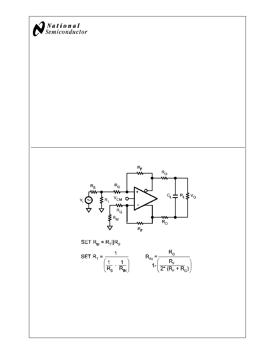
Typical Application
20133210
Single Ended Input Differential Output.
Gain = A
V
=R
F
/R
G
Where V
IN
is measured single ended and V
OUT
is measured differentially. (Each individual output will equal
±
V
IN
/2.)
LMH
TM
is a trademark of National Semiconductor Corporation.
February 2005
LMH6551
Differential,
High
Speed
Op
Amp
© 2005 National Semiconductor Corporation
DS201332
www.national.com
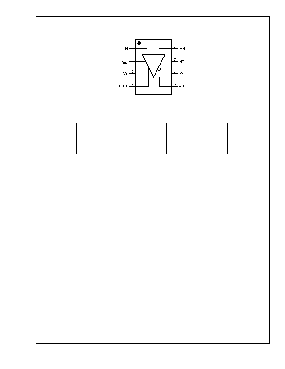
Connection Diagram
8-Pin SOIC & MSOP
20133208
Top View
Ordering Information
Package
Part Number
Package Marking
Transport Media
NSC Drawing
8-Pin SOIC
LMH6551MA
LMH6551MA
95/Rails
M08A
LMH6551MAX
2.5k Units Tape and Reel
8≠Pin MSOP
LMH6551MM
AU1A
1k Units Tape and Reel
MUA08A
LMH6551MMX
3.5k Units Tape and Reel
LMH6551
www.national.com
2
Absolute Maximum Ratings
(Note 1)
If Military/Aerospace specified devices are required,
please contact the National Semiconductor Sales Office/
Distributors for availability and specifications.
ESD Tolerance (Note 5)
Human Body Model
2000V
Machine Model
200V
Supply Voltage
13.2V
Common Mode Input Voltage
±
Vs
Maximum Input Current (pins 1, 2,
7, 8)
30mA
Maximum Output Current (pins 4, 5)
(Note 3)
Soldering Information
Infrared or Convection (20 sec)
235∞C
Wave Soldering (10 sec)
260∞C
Operating Ratings
(Note 1)
Operating Temperature Range
-40∞C to +125∞C
Storage Temperature Range
-65∞C to +150∞C
Total Supply Voltage
3V to 12V
Package Thermal Resistance (
JA
) (Note 4)
8-Pin MSOP
235∞C/W
8-Pin SOIC
150∞C/W
±
5V Electrical Characteristics
(Note 2)
Single ended in differential out, T
A
= 25∞C, G = +1, V
S
=
±
5V, V
CM
= 0V, R
F
= R
G
= 365
, R
L
= 500
;; Unless specified Bold-
face limits apply at the temperature extremes.
Symbol
Parameter
Conditions
Min
(Note 8)
Typ
(Note 7)
Max
(Note 8)
Units
AC Performance (Differential)
SSBW
Small Signal -3 dB Bandwidth
V
OUT
= 0.5 V
PP
370
MHz
LSBW
Large Signal -3 dB Bandwidth
V
OUT
= 2 V
PP
340
MHz
Large Signal -3 dB Bandwidth
V
OUT
= 4 V
PP
320
MHz
0.1 dB Bandwidth
V
OUT
= 2 V
PP
50
MHz
Slew Rate
4V Step(Note 6)
2400
V/µs
Rise/Fall Time
2V Step
1.8
ns
Settling Time
2V Step, 0.05%
18
ns
V
CM
Pin AC Performance (Common Mode Feedback Amplifier)
Common Mode Small Signal
Bandwidth
V
CM
bypass capacitor removed
200
MHz
Distortion and Noise Response
HD2
V
O
= 2 V
PP
, f = 5 MHz, R
L
=800
-94
dBc
HD2
V
O
= 2 V
PP
, f = 20MHz, R
L
=800
-85
dBc
HD3
V
O
= 2 V
PP
, f = 5 MHz, R
L
=800
-96
dBc
HD3
V
O
= 2 V
PP
, f = 20 MHz, R
L
=800
-72
dBc
e
n
Input Referred Voltage Noise
Freq
1 MHz
6.0
nV/
i
n
Input Referred Noise Current
Freq
1 MHz
1.5
pA/
Input Characteristics (Differential)
V
OSD
Input Offset Voltage
Differential Mode, V
ID
= 0, V
CM
= 0
0.5
±
4
±
6
mV
Input Offset Voltage Average
Temperature Drift
(Note 10)
-0.8
µV/∞C
I
BI
Input Bias Current
(Note 9)
-4
0
-10
µA
Input Bias Current Average
Temperature Drift
(Note 10)
-2.6
nA/∞C
Input Bias Difference
Difference in Bias currents
between the two inputs
0.03
µA
CMRR
Common Mode Rejection Ratio
DC, V
CM
= 0V, V
ID
= 0V
72
80
dBc
R
IN
Input Resistance
Differential
5
M
C
IN
Input Capacitance
Differential
1
pF
CMVR
Input Common Mode Voltage
Range
CMRR
>
53dB
+3.1
-4.6
+3.2
-4.7
V
V
CM
Pin Input Characteristics (Common Mode Feedback Amplifier)
LMH6551
www.national.com
3
±
5V Electrical Characteristics
(Note 2) (Continued)
Single ended in differential out, T
A
= 25∞C, G = +1, V
S
=
±
5V, V
CM
= 0V, R
F
= R
G
= 365
, R
L
= 500
;; Unless specified Bold-
face limits apply at the temperature extremes.
Symbol
Parameter
Conditions
Min
(Note 8)
Typ
(Note 7)
Max
(Note 8)
Units
V
OSC
Input Offset Voltage
Common Mode, V
ID
= 0
0.5
±
5
±
8
mV
Input Offset Voltage Average
Temperature Drift
(Note 10)
8.2
µV/∞C
Input Bias Current
(Note 9)
-2
µA
V
CM
CMRR
V
ID
= 0V, 1V step on V
CM
pin,
measure V
OD
70
75
dB
Input Resistance
25
k
Common Mode Gain
V
O,CM
/
V
CM
0.995
0.999
1.005
V/V
Output Performance
Output Voltage Swing
Single Ended, Peak to Peak
±
7.38
±
7.18
±
7.8
V
Output Common Mode Voltage
Range
V
ID
= 0 V,
±
3.69
±
3.8
V
I
OUT
Linear Output Current
V
OUT
= 0V
±
50
±
65
mA
I
SC
Short Circuit Current
Output Shorted to Ground
V
IN
= 3V Single Ended(Note 3)l
140
mA
Output Balance Error
V
OUT
Common Mode
/
V
OUT
DIfferential , V
OUT
= 0.5
Vpp Differential, f = 10 MHz
-70
dB
Miscellaneous Performance
A
VOL
Open Loop Gain
Differential
70
dB
PSRR
Power Supply Rejection Ratio
DC,
V
S
=
±
1V
74
90
dB
Supply Current
R
L
=
11
12.5
14.5
16.5
mA
5V Electrical Characteristics
(Note 2)
Single ended in differential out, T
A
= 25∞C, G = +1, V
S
= 5V, V
CM
= 2.5V, R
F
= R
G
= 365
, R
L
= 500
; ; Unless specifiedBold-
face limits apply at the temperature extremes.
Symbol
Parameter
Conditions
Min
(Note 8)
Typ
(Note 7)
Max
(Note 8)
Units
SSBW
Small Signal -3 dB Bandwidth
R
L
= 500
, V
OUT
= 0.5 V
PP
350
MHz
LSBW
Large Signal -3 dB Bandwidth
R
L
= 500
, V
OUT
= 2 V
PP
300
MHz
0.1 dB Bandwidth
V
OUT
= 2 V
PP
50
MHz
Slew Rate
4V Step(Note 6)
1800
V/µs
Rise/Fall Time, 10% to 90%
4V Step
2
ns
Settling Time
4V Step, 0.05%
17
ns
V
CM
Pin AC Performance (Common Mode Feedback Amplifier)
Common Mode Small Signal
Bandwidth
170
MHz
Distortion and Noise Response
HD2
2
nd
Harmonic Distortion
V
O
= 2 V
PP
, f = 5 MHz, R
L
=800
-84
dBc
HD2
V
O
= 2 V
PP
, f = 20 MHz, R
L
=800
-69
dBc
HD3
3
rd
Harmonic Distortion
V
O
= 2 V
PP
, f = 5 MHz, R
L
=800
-93
dBc
HD3
V
O
= 2 V
PP
, f = 20 MHz, R
L
=800
-67
dBc
e
n
Input Referred Noise Voltage
Freq
1 MHz
6.0
nV/
i
n
Input Referred Noise Current
Freq
1 MHz
1.5
pA/
Input Characteristics (Differential)
LMH6551
www.national.com
4
5V Electrical Characteristics
(Note 2) (Continued)
Single ended in differential out, T
A
= 25∞C, G = +1, V
S
= 5V, V
CM
= 2.5V, R
F
= R
G
= 365
, R
L
= 500
; ; Unless specifiedBold-
face limits apply at the temperature extremes.
Symbol
Parameter
Conditions
Min
(Note 8)
Typ
(Note 7)
Max
(Note 8)
Units
V
OSD
Input Offset Voltage
Differential Mode, V
ID
= 0, V
CM
= 0
0.5
±
4
±
6
mV
Input Offset Voltage Average
Temperature Drift
(Note 10)
-0.8
µV/∞C
I
BIAS
Input Bias Current
(Note 9)
-4
0
-10
µA
Input Bias Current Average
Temperature Drift
(Note 10)
-3
nA/∞C
Input Bias Current Difference
Difference in Bias currents between
the two inputs
0.03
µA
CMRR
Common-Mode Rejection Ratio
DC, V
ID
= 0V
70
78
dBc
Input Resistance
Differential
5
M
Input Capacitance
Differential
1
pF
V
ICM
Input Common Mode Range
CMRR
>
53 dB
+3.1
+0.4
+3.2
+0.3
V
CM
Pin Input Characteristics (Common Mode Feedback Amplifier)
Input Offset Voltage
Common Mode, V
ID
= 0
0.5
±
5
±
8
mV
Input Offset Voltage Average
Temperature Drift
5.8
µV/∞C
Input Bias Current
3
µA
V
CM
CMRR
V
ID
= 0,
1V step on V
CM
pin, measure V
OD
70
75
dB
Input Resistance
V
CM
pin to ground
25
k
Common Mode Gain
V
O,CM
/
V
CM
0.995
0.991
1.005
V/V
Output Performance
V
OUT
Output Voltage Swing
Single Ended, Peak to Peak, V
S
=
±
2.5V, V
CM
= 0V
±
2.4
±
2.8
V
I
OUT
Linear Output Current
V
OUT
= 0V Differential
±
45
±
60
mA
I
SC
Output Short Circuit Current
Output Shorted to Ground
V
IN
= 3V Single Ended(Note 3)
230
mA
CMVR
Output Common Mode Voltage
Range
V
ID
= 0, V
CM
pin = 1.2V and 3.8V
3.72
1.23
3.8
1.2
V
Output Balance Error
V
OUT
Common Mode
/
V
OUT
DIfferential , V
OUT
= 1Vpp
Differential, f = 10 MHz
-65
dB
Miscellaneous Performance
Open Loop Gain
DC, Differential
70
dB
PSRR
Power Supply Rejection Ratio
DC,
V
S
=
±
0.5V
72
88
dB
I
S
Supply Current
R
L
=
10
11.5
13.5
15.5
mA
3.3V Electrical Characteristics
(Note 2)
Single ended in differential out, T
A
= 25∞C, G = +1, V
S
= 3.3V, V
CM
= 1.65V, R
F
= R
G
= 365
, R
L
= 500
; ; Unless specified-
Boldface limits apply at the temperature extremes.
Symbol
Parameter
Conditions
Min
(Note 8)
Typ
(Note 7)
Max
(Note 8)
Units
SSBW
Small Signal -3 dB Bandwidth
R
L
= 500
, V
OUT
= 0.5 V
PP
320
MHz
LMH6551
www.national.com
5