 | –≠–ª–µ–∫—Ç—Ä–æ–Ω–Ω—ã–π –∫–æ–º–ø–æ–Ω–µ–Ω—Ç: LMH6559MF | –°–∫–∞—á–∞—Ç—å:  PDF PDF  ZIP ZIP |
LMH6559
High-Speed, Closed-Loop Buffer
General Description
The LMH6559 is a high-speed, closed-loop buffer designed
for applications requiring the processing of very high fre-
quency signals. While offering a small signal bandwidth of
1750MHz, and an ultra high slew rate of 4580V/µs the
LMH6559 consumes only 10mA of quiescent current. Total
harmonic distortion into a load of 100
at 20MHz is -52dBc.
The LMH6559 is configured internally for a loop gain of one.
Input resistance is 200k
and output resistance is but 1.2.
These characteristics make the LMH6559 an ideal choice for
the distribution of high frequency signals on printed circuit
boards. Differential gain and phase specifications of 0.06%
and 0.02∞ respectively at 3.58MHz make the LMH6559 well
suited for the buffering of video signals.
The device is fabricated on National's high-speed VIP10
process using National's proven high performance circuit
architectures.
Features
n
Closed-loop buffer
n
1750MHz small signal bandwidth
n
4580V/µs slew rate
n
0.06% / 0.02∞ differential gain/phase
n
-52dBc THD at 20MHz
n
Single supply operation (3V min.)
n
75mA output current
Applications
n
Video switching and routing
n
Test point drivers
n
High frequency active filters
n
Wideband DC clamping buffers
n
High-speed peak detector circuits
n
Transmission systems
n
Telecommunications
n
Test equipment and instrumentation
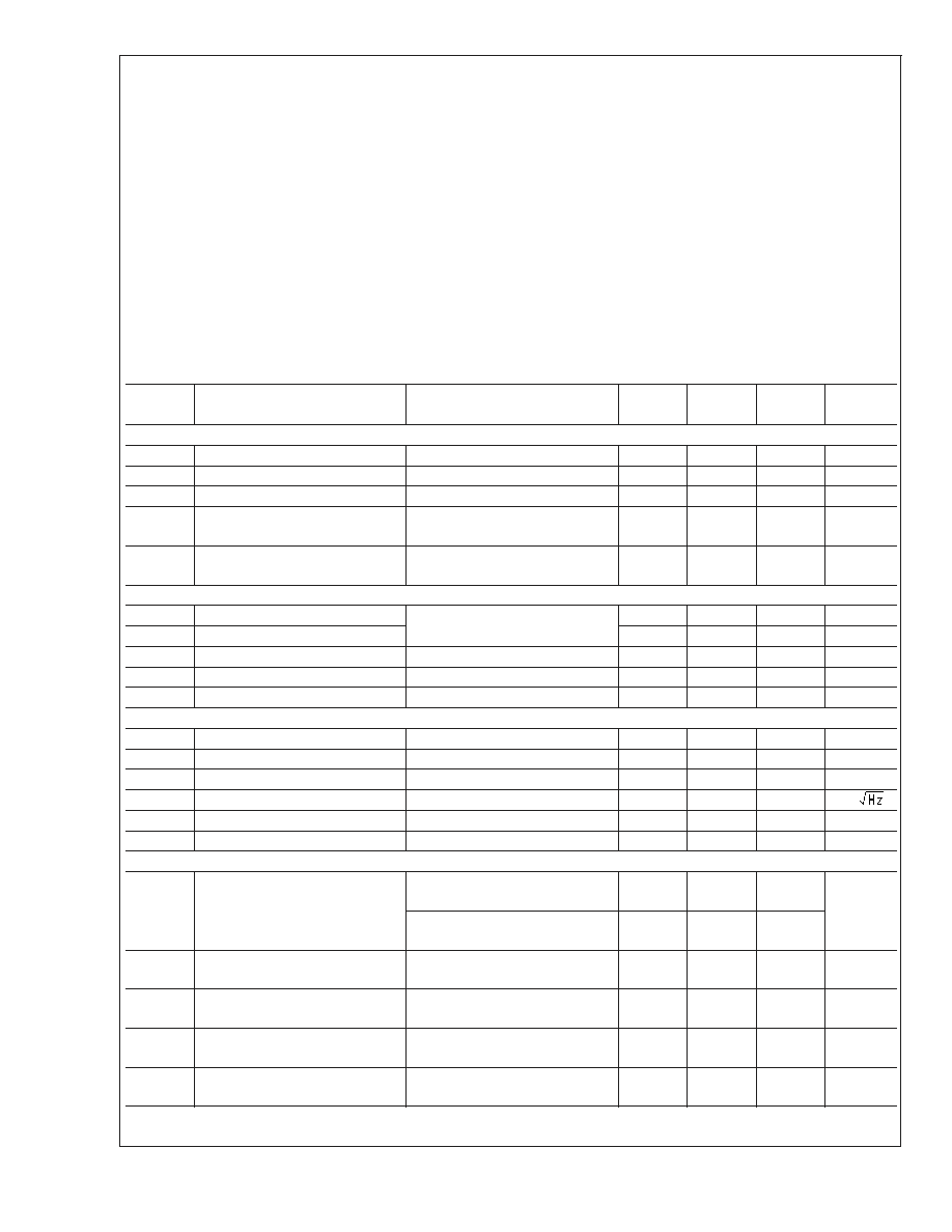
Typical Schematic
20064133
April 2003
LMH6559
High-Speed,
Closed-Loop
Buffer
© 2003 National Semiconductor Corporation
DS200641
www.national.com
Absolute Maximum Ratings
(Note 1)
If Military/Aerospace specified devices are required,
please contact the National Semiconductor Sales Office/
Distributors for availability and specifications.
ESD Tolerance
Human Body Model
2000V (Note 2)
Machine Model
200V (Note 3)
Output Short Circuit Duration
(Note 4), (Note 5)
Supply Voltage (V
+
≠ V
-
)
13V
Voltage at Input/Output Pins
V
+
+0.8V, V
-
-0.8V
Soldering Information
Infrared or Convection (20 sec.)
235∞C
Wave Soldering (10 sec.)
260∞C
Storage Temperature Range
-65∞C to +150∞C
Junction Temperature
+150∞C
Operating Ratings
(Note 1)
Supply Voltage (V
+
- V
-
)
3 - 10V
Operating Temperature
Range (Note 6), (Note 7)
-40∞C to +85∞C
Package Thermal Resistance (Note 6), (Note 7)
8-Pin SOIC
172∞C/W
5-Pin SOT23
235∞C/W
±
5V Electrical Characteristics
Unless otherwise specified, all limits guaranteed for T
J
= 25∞C, V
+
= +5V, V
-
= -5V, V
O
= V
CM
= 0V and R
L
= 100
to 0V.
Boldface limits apply at the temperature extremes.
Symbol
Parameter
Conditions
Min
(Note 9)
Typ
(Note 8)
Max
(Note 9)
Units
Frequency Domain Response
SSBW
Small Signal Bandwidth
V
O
<
0.5V
PP
1750
MHz
GFN
Gain Flatness
<
0.1dB
V
O
<
0.5V
PP
200
MHz
FPBW
Full Power Bandwidth (-3dB)
V
O
= 2V
PP
(+10dBm)
1050
MHZ
DG
Differential Gain
R
L
= 150
to 0V;
f = 3.58 MHz
0.06
%
DP
Differential Phase
R
L
= 150
to 0V;
f = 3.58 MHz
0.02
deg
Time Domain Response
t
r
Rise Time
3.3V Step (20-80%)
0.4
ns
t
f
Fall Time
0.5
ns
t
s
Settling Time to
±
0.1%
3.3V Step
9
ns
OS
Overshoot
1V Step
4
%
SR
Slew Rate
(Note 11)
4580
V/µs
Distortion And Noise Performance
HD2
2
nd
Harmonic Distortion
V
O
= 2V
PP
; f = 20MHz
-58
dBc
HD3
3
rd
Harmonic Distortion
V
O
= 2V
PP
; f = 20MHz
-53
dBc
THD
Total Harmonic Distortion
V
O
= 2V
PP
; f = 20MHz
-52
dBc
e
n
Input-Referred Voltage Noise
f = 1MHz
2.8
nV/
CP
1dB Compression point
f = 10MHz
+23
dBm
SNR
Signal to Noise Ratio
f = 5MHz; V
O
= 1V
PP
120
dB
Static, DC Performance
A
CL
Small Signal Voltage Gain
V
O
= 100mV
PP
R
L
= 100
to 0V
.97
.996
V/V
V
O
= 100mV
PP
R
L
= 2k
to 0V
.99
.998
V
OS
Input Offset Voltage
3
20
25
mV
TC V
OS
Temperature Coefficient Input
Offset Voltage
(Note 12)
23
µV/∞C
I
B
Input Bias Current
(Note 10)
-10
-14
-3
µA
TC I
B
Temperature Coefficient Input
Bias Current
(Note 12)
-3.6
nA/∞C
LMH6559
www.national.com
2
±
5V Electrical Characteristics
(Continued)
Unless otherwise specified, all limits guaranteed for T
J
= 25∞C, V
+
= +5V, V
-
= -5V, V
O
= V
CM
= 0V and R
L
= 100
to 0V.
Boldface limits apply at the temperature extremes.
Symbol
Parameter
Conditions
Min
(Note 9)
Typ
(Note 8)
Max
(Note 9)
Units
R
OUT
Output Resistance
R
L
= 100
to 0V; f = 100kHz
1.2
R
L
= 100
to 0V; f = 10MHz
1.3
PSRR
Power Supply Rejection Ratio
V
S
=
±
5V to V
S
=
±
5.25V
48
44
63
dB
I
S
Supply Current
No Load
10
14
17
mA
Miscellaneous Performance
R
IN
Input Resistance
200
k
C
IN
Input Capacitance
1.7
pF
V
O
Output Swing Positive
R
L
= 100
to 0V
3.20
3.18
3.45
V
R
L
= 2k
to 0V
3.55
3.54
3.65
Output Swing Negative
R
L
= 100
to 0V
-3.45
-3.20
-3.18
V
R
L
= 2k
to 0V
-3.65
-3.55
-3.54
I
SC
Output Short Circuit Current
Sourcing: V
IN
= +V
S
; V
O
= 0V
-83
mA
Sinking: V
IN
= -V
S
; V
O
= 0V
83
I
O
Linear Output Current
Sourcing: V
IN
- V
O
= 0.5V
(Note 10)
-50
-43
-74
mA
Sinking: V
IN
- V
O
= -0.5V
(Note 10)
50
43
74
5V Electrical Characteristics
Unless otherwise specified, all limits guaranteed for T
J
= 25∞C, V
+
= 5V, V
-
= 0V, V
O
= V
CM
= V
+
/2 and R
L
= 100
to V
+
/2.
Boldface limits apply at the temperature extremes.
Symbol
Parameter
Conditions
Min
(Note 9)
Typ
(Note 8)
Max
(Note 9)
Units
Frequency Domain Response
SSBW
Small Signal Bandwidth
V
O
<
0.5V
PP
745
MHz
GFN
Gain Flatness
<
0.1dB
V
O
<
0.5V
PP
90
MHz
FPBW
Full Power Bandwidth (-3dB)
V
O
= 2V
PP
(+10dBm)
485
MHZ
DG
Differential Gain
R
L
= 150
to V
+
/2;
f = 3.58 MHz
0.29
%
DP
Differential Phase
R
L
= 150
to V
+
/2;
f = 3.58 MHz
0.06
deg
Time Domain Response
t
r
Rise Time
2.3V
PP
Step (20-80%)
0.6
ns
t
f
Fall Time
0.9
ns
t
s
Settling Time to
±
0.1%
2.3V Step
9.6
ns
OS
Overshoot
1V Step
3
%
SR
Slew Rate
(Note 11)
2070
V/µs
Distortion And Noise Performance
HD2
2
nd
Harmonic Distortion
V
O
= 2V
PP
; f = 20MHz
-53
dBc
HD3
3
rd
Harmonic Distortion
V
O
= 2V
PP
; f = 20MHz
-56
dBc
THD
Total Harmonic Distortion
V
O
= 2V
PP
; f = 20MHz
-52
dBc
e
n
Input-Referred Voltage Noise
f = 1MHz
2
nV/
LMH6559
www.national.com
3

5V Electrical Characteristics
(Continued)
Unless otherwise specified, all limits guaranteed for T
J
= 25∞C, V
+
= 5V, V
-
= 0V, V
O
= V
CM
= V
+
/2 and R
L
= 100
to V
+
/2.
Boldface limits apply at the temperature extremes.
Symbol
Parameter
Conditions
Min
(Note 9)
Typ
(Note 8)
Max
(Note 9)
Units
CP
1dB Compression point
f = 10MHz
+7
dBm
SNR
Signal to Noise Ratio
f = 5MHz; V
O
= 1V
PP
123
dB
Static, DC Performance
A
CL
Small Signal Voltage Gain
V
O
= 100mV
PP
R
L
= 100
to V
+
/2
.97
.996
V/V
V
O
= 100mV
PP
R
L
= 2k
to V
+
/2
.99
.998
V
OS
Input Offset Voltage
1.52
12
16
mV
TC V
OS
Temperature Coefficient Input
Offset Voltage
(Note 12)
23
µV/∞C
I
B
Input Bias Current
(Note 10)
-5
-8
-2.7
µA
TC I
B
Temperature Coefficient Input
Bias Current
(Note 12)
1.6
nA/∞C
R
OUT
Output Resistance
R
L
= 100
to V
+
/2; f = 100kHz
1.4
R
L
= 100
to V
+
/2; f = 10MHz
1.6
PSRR
Power Supply Rejection Ratio
V
S
= +5V to V
S
= +5.5V;
V
IN
= V
S
/2
48
44
68
dB
I
S
Supply Current
No Load
4.7
7
8.5
mA
Miscellaneous Performance
R
IN
Input Resistance
22
k
C
IN
Input Capacitance
2.0
pF
V
O
Output Swing Positive
R
L
= 100
to V
+
/2
3.80
3.75
3.88
V
R
L
= 2k
to V
+
/2
3.94
3.92
3.98
Output Swing Negative
R
L
= 100
to V
+
/2
1.12
1.20
1.25
V
R
L
= 2k
to V
+
/2
1.03
1.06
1.09
I
SC
Output short circuit Current
Sourcing: V
IN
= +V
S
; V
O
= V
+
/2
-57
mA
Sinking: V
IN
= -V
S
; V
O
= V
+
/2
26
I
O
Linear Output Current
Sourcing: V
IN
- V
O
= 0.5V
(Note 10)
-50
-43
-64
mA
Sinking: V
IN
- V
O
= -0.5V
(Note 10)
30
23
42
3V Electrical Characteristics
Unless otherwise specified, all limits guaranteed for T
J
= 25∞C, V
+
= 3V, V
-
= 0V, V
O
= V
CM
= V
+
/2 and R
L
= 100
to V
+
/2.
Boldface limits apply at the temperature extremes.
Symbol
Parameter
Conditions
Min
(Note 9)
Typ
(Note 8)
Max
(Note 9)
Units
Frequency Domain Response
SSBW
Small Signal Bandwidth
V
O
<
0.5V
PP
315
MHz
GFN
Gain Flatness
<
0.1dB
V
O
<
0.5V
PP
44
MHz
FPBW
Full Power Bandwidth (-3dB)
V
O
= 1V
PP
(+4.5dBm)
265
MHZ
LMH6559
www.national.com
4
3V Electrical Characteristics
(Continued)
Unless otherwise specified, all limits guaranteed for T
J
= 25∞C, V
+
= 3V, V
-
= 0V, V
O
= V
CM
= V
+
/2 and R
L
= 100
to V
+
/2.
Boldface limits apply at the temperature extremes.
Symbol
Parameter
Conditions
Min
(Note 9)
Typ
(Note 8)
Max
(Note 9)
Units
Time Domain Response
t
r
Rise Time
1.0V Step (20-80%)
0.8
ns
t
f
Fall Time
1.2
ns
t
s
Settling Time to
±
0.1%
1V Step
10
ns
OS
Overshoot
0.5V Step
0
%
SR
Slew Rate
(Note 11)
770
V/µs
Distortion And Noise Performance
HD2
2
nd
Harmonic Distortion
V
O
= 2V
PP
; f = 20MHz
-74
dBc
HD3
3
rd
Harmonic Distortion
V
O
= 2V
PP
; f = 20MHz
-57
dBc
THD
Total Harmonic Distortion
V
O
= 2V
PP
; f = 20MHz
-56
dBc
e
n
Input-Referred Voltage Noise
f = 1MHz
2
nV/
CP
1dB Compression point
f = 10MHz
+4
dBm
SNR
Signal to Noise Ratio
f = 5MHz; V
O
= 1V
PP
124
dB
Static, DC Performance
A
CL
Small Signal Voltage Gain
V
O
= 100mV
PP
R
L
= 100
to V
+
/2
.97
.995
V/V
V
O
= 100mV
PP
R
L
= 2k
to V
+
/2
.99
.998
V
OS
Input Offset Voltage
1
7
9
mV
TC V
OS
Temperature Coefficient Input
Offset Voltage
(Note 12)
3.5
µV/∞C
I
B
Input Bias Current
(Note 10)
-3
-3.5
-1.5
µA
TC I
B
Temperature Coefficient Input
Bias Current
(Note 12)
0.46
nA/∞C
R
OUT
Output Resistance
R
L
= 100
to V
+
/2; f = 100kHz
1.8
R
L
= 100
to V
+
/2; f = 10MHz
2.3
PSRR
Power Supply Rejection Ratio
V
S
= +3V to V
S
= +3.5V;
V
IN
= V
+
/2
48
46
68
dB
I
S
Supply Current
No Load
2.4
3.5
4.5
mA
Miscellaneous Performance
R
IN
Input Resistance
23
k
C
IN
Input Capacitance
2.3
pF
V
O
Output Swing Positive
R
L
= 100
to V
+
/2
2.02
1.95
2.07
V
R
L
= 2k
to V
+
/2
2.12
2.02
2.17
Output Swing Negative
R
L
= 100
to V
+
/2
.930
.970
1.050
V
R
L
= 2k
to V
+
/2
.830
.880
.980
I
SC
Output Short Circuit Current
Sourcing: V
IN
= +V
S
; V
O
= V
+
/2
-32
mA
Sinking: V
IN
= -V
S
; V
O
= V
+
/2
15
LMH6559
www.national.com
5