 | –≠–ª–µ–∫—Ç—Ä–æ–Ω–Ω—ã–π –∫–æ–º–ø–æ–Ω–µ–Ω—Ç: LMH6572 | –°–∫–∞—á–∞—Ç—å:  PDF PDF  ZIP ZIP |
LMH6572
Triple 2:1 High Speed Video Multiplexer
General Description
The LMH
TM
6572 is a high performance analog mulitplexer
optimized for professional grade video and other high fidelity
high bandwidth analog applications. The LMH6572 provides
a 290MHz bandwidth at 2 V
PP
output signal levels. The 140
MHz of .1 dB bandwidth and a 1500 V/µs slew rate make this
part suitable for High Definition Television (HDTV) and High
Resolution Multimedia Video applications.
The LMH6572 supports composite video applications with its
0.02% and 0.02∞ differential gain and phase errors for NTSC
and PAL video signals while driving a single, back terminated
75
load. The LMH6572 can deliver 80 mA linear output
current for driving multiple video load applications.
The LMH6572 has an internal gain of two for driving back
terminated transmission lines at a net gain of one.
The LMH6572 is available in the SSOP package.
Features
n
350 MHz, 250 mV -3 dB bandwidth
n
290 MHz, 2 V
PP
-3 dB bandwidth
n
10 ns channel switching time
n
90 dB channel to channel isolation
@
5 MHz
n
0.02%, 0.02∞ diff. gain, phase
n
.1 dB gain flatness to 140 MHz
n
1400 V/µs slew rate
n
Wide supply voltage range: 6V (
±
3V) to 12V (
±
6V)
n
-78 dB HD2
@
10MHz
n
-75 dB HD3
@
10MHz
Applications
n
RGB video router
n
Multi input video monitor
n
Fault tolerant data switch
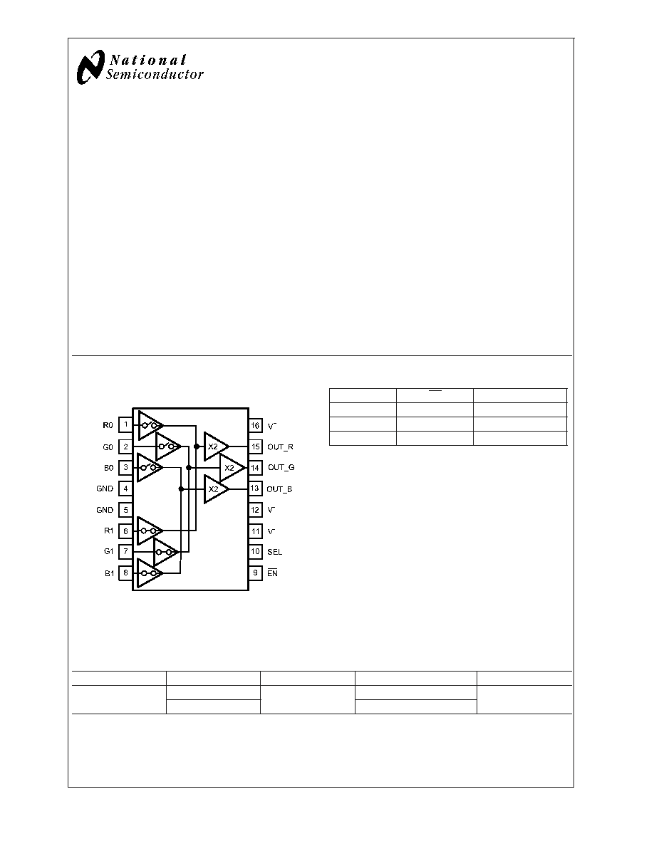
Connection Diagram
16-Pin SSOP
20109605
Top View
Truth Table
SEL
EN
OUT
0
0
CH 1
1
0
CH 0
X
1
Disable
Ordering Information
Package
Part Number
Package Marking
Transport Media
NSC Drawing
16-Pin SSOP
LMH6572MQ
LH6572MQ
95 Units/Rail
MQA16
LMH6572MQX
2.5 Units Tape and Reel
LMH
TM
is a trademark of National Semiconductor Corporation.
August 2004
LMH6572
T
riple
2:1
High
Speed
V
ideo
Multiplexer
© 2004 National Semiconductor Corporation
DS201096
www.national.com
Absolute Maximum Ratings
(Note 1)
If Military/Aerospace specified devices are required,
please contact the National Semiconductor Sales Office/
Distributors for availability and specifications.
ESD Tolerance
(Note 4)
Human Body Model
2000V
Machine Model
200V
Supply Voltage (V
+
- V
-
)
13.2V
I
OUT
(Note 3)
130 mA
IInput Voltage Range
±
V
S
Maximum Junction Temperature
+150∞C (Note 4)
Storage Temperature Range
-65∞C to +150∞C
Soldering Information
Infrared or Convection (20 sec)
235∞C
Wave Soldering (10 sec)
260∞C
Operating Ratings
(Note 1)
Operating Temperature
-40∞C
to
85∞C
Supply Voltage Range
6V
to
12V
Thermal Resistance
Package
(
JA
)
(
JC
)
16-Pin SSOP
125∞C/W
36∞C/W
±
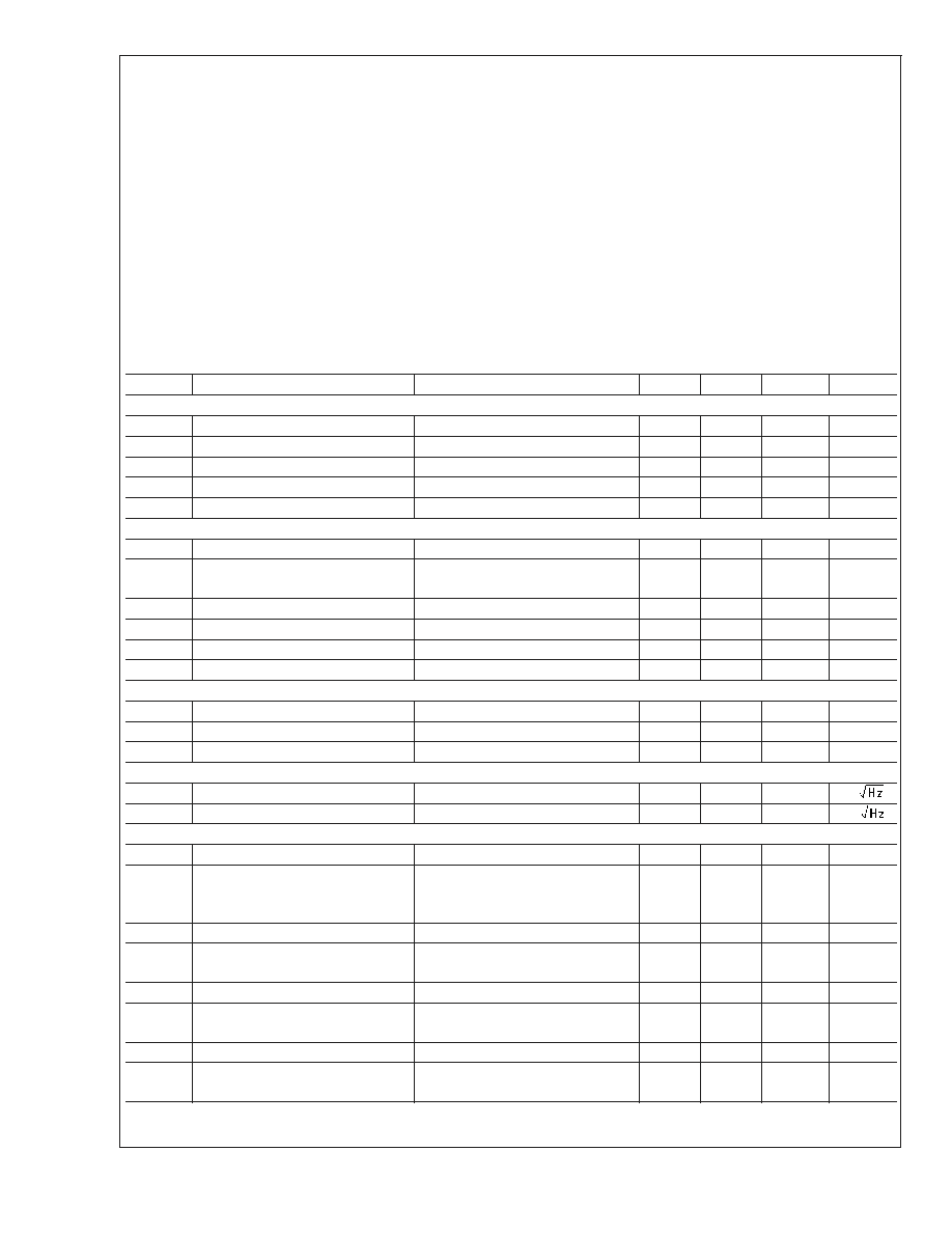
5V Electrical Characteristics
V
S
=
±
5V, R
L
= 100
, Unless otherwise specified.
Symbol
Parameter
Conditions(Note 2)
Min
Typ
Max
Units
Frequency Domain Performance
SSBW
-3 dB Bandwidth
V
OUT
= 0.25 V
PP
350
MHz
LSBW
≠3 dB Bandwidth (Note 6)
V
OUT
= 2 V
PP
250
290
MHz
.1 dBBW
. 1 dB Bandwidth
V
OUT
= 0.25 V
PP
140
MHz
DG
Differential Gain
R
L
= 150
, f=4.43 MHz
0.02
%
DP
Differential Phase
R
L
= 150
, f=4.43 MHz
0.02
deg
Time Domain Response
TRS
Channel to Channel Switching Time
Logic transition to 90% output
10
ns
Enable and Disable Times
Logic transition to 90% or 10%
output.
11
ns
TRL
Rise and Fall Time
2V Step
1.5
ns
TSS
Settling Time to 0.05%
2V Step
17
ns
OS
Overshoot
4V Step
5
%
SR
Slew Rate(Note 6)
4V Step
1200
1400
V/µs
Distortion
HD2
2
nd
Harmonic Distortion
2 V
PP
, 10 MHz
-78
dBc
HD3
3
rd
Harmonic Distortion
2 V
PP
, 10 MHz
-75
dBc
IMD
3
rd
Order Intermodulation Products
10 MHz, Two tones 2Vpp at output
-80
dBc
Equivalent Input Noise
VN
Voltage
>
1 MHz, Input Referred
5
nV
ICN
Current
>
1 MHz, Input Referred
5
pA/
Static, DC Performance
GAIN
Voltage Gain (Note 5)
No Load
1.9
2.0
2.1
V/V
Gain Error(Note 5)
No Load, channel to channel
±
0.3
±
0.5
±
0.7
%
Gain Error
R
L
= 50
0.3
%
VIO
Output Offset Voltage (Note 5)
V
IN
= 0V
1
±
14
±
17.5
mV
DVIO
Average Drift
27
µV/∞C
IBN
Input Bias Current (Notes 7, 5)
V
IN
= 0V
-1.4
±
2.8
±
3.5
µA
DIBN
Average Drift
7
nA/∞C
PSRR
Power Supply Rejection Ratio
(Note 5)
DC, Input referred
50
48
54
dB
LMH6572
www.national.com
2
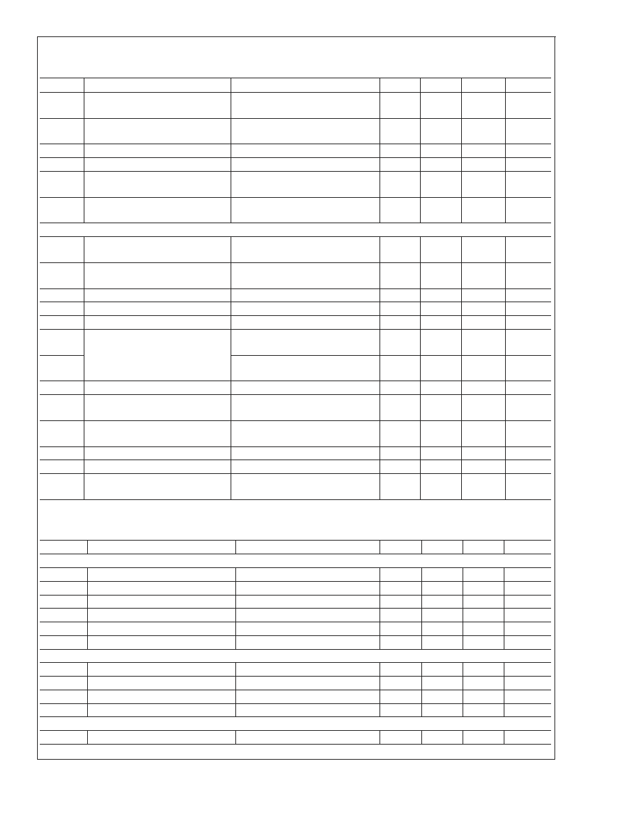
±
5V Electrical Characteristics
(Continued)
V
S
=
±
5V, R
L
= 100
, Unless otherwise specified.
Symbol
Parameter
Conditions(Note 2)
Min
Typ
Max
Units
ICC
Supply Current (Note 5)
No Load
20
23
25
28.5
mA
Supply Current Disabled(Note 5)
No Load
2.0
2.2
2.3
mA
VIH
Logic High Threshold(Note 5)
Select & Enable Pins
2.0
V
VIL
Logic Low Threshold (Note 5)
Select & Enable Pins
0.8
V
IiL
Logic Pin Input Current Low(Note 7) Logic Input = 0V
-1
±
2.5
±
10
µA
IiH
Logic Pin Input Current High(Note
7)
Logic Input = 2.0V
112
100
150
200
210
µA
Miscellaneous Performance
RF
Internal Feedback and Gain Set
resistor Values
650
620
800
940
1010
RODIS
Disabled Output Resistance
Internal Feedback and Gain Set
resistors in series to ground.
1.3
1.6
1.88
k
RIN+
Input Resistance
100
k
CIN
Input Capacitance
0.9
pF
ROUT
Output Resistance
0.26
VO
Output Voltage Range
No Load
±
3.83
±
3.80
±
3.9
V
VOL
R
L
= 100
±
3.52
±
3.5
±
3.53
V
CMIR
Input Voltage Range
±
2
±
2.5
V
IO
Linear Output Current (Notes 5, 7)
V
IN
= 0V,
+70
-40
±
80
mA
ISC
Short Circuit Current
V
IN
=
±
2V, Output shorted to
ground
±
230
mA
XTLK
Channel to Channel Crosstalk
V
IN
= 2 V
PP
@
5 MHz
-90
dBc
XTLK
Channel to Channel Crosstalk
V
IN
= 2 V
PP
@
100 MHZ
-54
dBc
XTLK
All Hostile Crosstalk
In A, C. Out B, V
IN
= 2 V
PP
@
5
MHz
-95
dBc
±
3.3V Electrical Characteristics
V
S
=
±
3.3V, R
L
= 100
; Unless otherwise specified.
Symbol
Parameter
Conditions(Note 2)
Min
Typ
Max
Units
Frequency Domain Performance
SSBW
-3 dB Bandwidth
V
OUT
= 0.25 V
PP
360
MHz
LSBW
-3 dB Bandwidth
V
OUT
= 2.0 V
PP
270
MHz
.1 dBBW
.1 dB Bandwidth
V
OUT
= 0.5 V
PP
80
MHz
GFP
Peaking
DC to 200 MHz
0.3
dB
DG
Differential Gain
R
L
= 150
, f=4.43 MHz
0.02
%
DP
Differential Phase
R
L
= 150
, f=4.43 MHz
0.03
deg
Time Domain Response
TRS
Rise and Fall Time
2V Step
2.0
ns
TSS
Settling Time to 0.05%
2V Step
15
ns
OS
Overshoot
2V Step
5
%
SR
Slew Rate
2V Step
1000
V/µs
Distortion
HD2
2
nd
Harmonic Distortion
2 V
PP
, 10MHz
-70
dBc
LMH6572
www.national.com
3
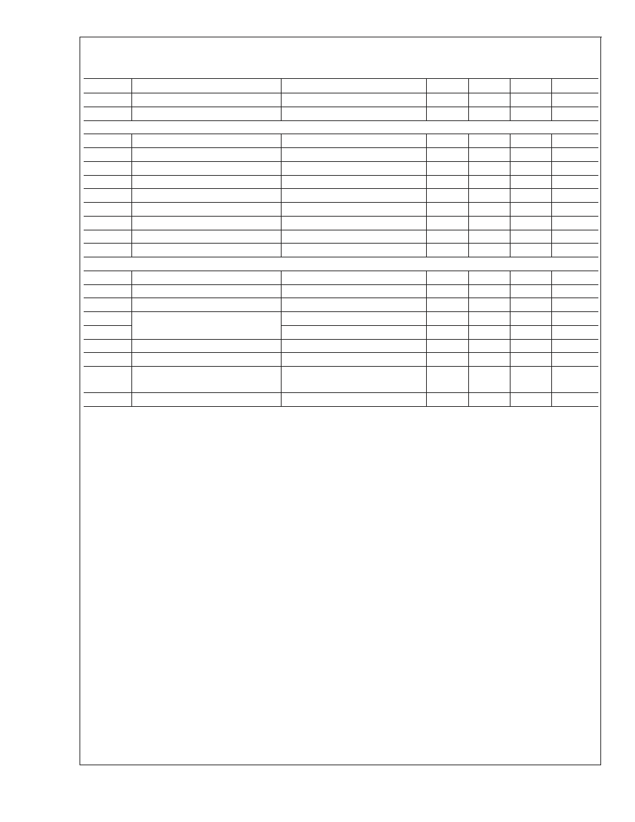
±
3.3V Electrical Characteristics
(Continued)
V
S
=
±
3.3V, R
L
= 100
; Unless otherwise specified.
Symbol
Parameter
Conditions(Note 2)
Min
Typ
Max
Units
HD3
3
rd
Harmonic Distortion
2 V
PP
, 10MHz
-74
dBc
IMD
3
rd
Order Intermodulation Products
10 MHz, Two tones 2Vpp at output
-79
dBc
Static, DC Performance
GAIN
Voltage Gain
2.0
V/V
VIO
Output Offset Voltage
V
IN
= 0V
1
mV
DVIO
Average Drift
36
µV/∞C
IBN
Input Bias Current (Note 7)
V
IN
= 0V
2
µA
DIBN
Average Drift
24
nA/∞C
PSRR
Power Supply Rejection Ratio
DC, Input Referred
54
dB
ICC
Supply Current
R
L
=
20
mA
VIH
Logic High Threshold
Select & Enable Pins
1.3
V
VIL
Logic Low Threshold
Select & Enable Pins
0.4
V
Miscellaneous Performance
RIN+
Input Resistance
100
k
CIN
Input Capacitance
0.9
pF
ROUT
Output Resistance
0.27
VO
Output Voltage Range
No Load
±
2.5
V
VOL
R
L
= 100
±
2.2
V
CMIR
Input Voltage Range
±
1.2
V
IO
Linear Output Current
V
IN
= 0V
±
60
mA
ISC
Short Circuit Current
V
IN
=
±
1V, Output shorted to
ground
±
150
mA
XTLK
Channel to Channel Crosstalk
5 MHz
-90
dBc
Note 1: Absolute Maximum Ratings indicate limits beyond which damage to the device may occur. Operating Ratings indicate conditions for which the device is
intended to be functional, but specific performance is not guaranteed. For guaranteed specifications, see the Electrical Characteristics tables.
Note 2: Electrical Table values apply only for factory testing conditions at the temperature indicated. Factory testing conditions result in very limited self-heating of
the device such that T
J
= T
A
. No guarantee of parametric performance is indicated in the electrical tables under conditions of internal self heating where T
J
>
T
A
.
See Applications Section for information on temperature de-rating of this device. Min/Max ratings are based on product testing, characterization and simulation.
Individual parameters are tested as noted.
Note 3: The maximum output current (I
OUT
) is determined by device power dissipation limitations. See the Power Dissipation section of the Application Section for
more details. A short circuit condition should be limited to 5 seconds or less.
Note 4: Human Body model, 1.5 k
in series with 100 pF. Machine model, 0 In series with 200 pF
Note 5: Parameters guaranteed by electrical testing at 25∞ C.
Note 6: Parameters guaranteed by design.
Note 7: Positive Value is current into device.
LMH6572
www.national.com
4
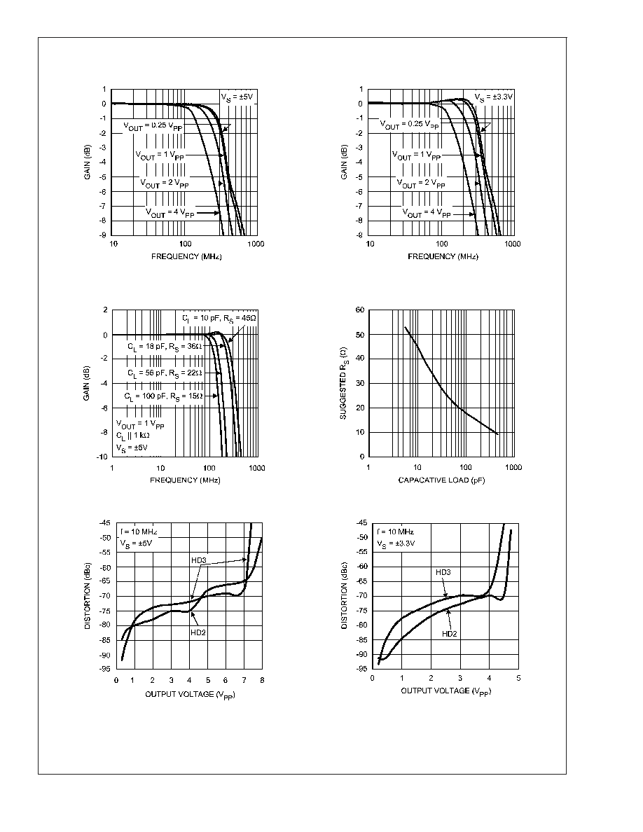
Typical Performance Characteristics
V
s
=
±
5V, R
L
= 100
; unless otherwise specified.
Frequency Response vs. V
OUT
Frequency Response vs. V
OUT
20109602
20109601
Frequency Response vs. Capacitive Load
Suggested R
S
vs. Capacitive Load
Load= 1k
i C
L
20109613
20109604
Harmonic Distortion vs. Output Voltage
Harmonic Distortion vs. Output Voltage
20109611
20109612
LMH6572
www.national.com
5