 | –≠–ª–µ–∫—Ç—Ä–æ–Ω–Ω—ã–π –∫–æ–º–ø–æ–Ω–µ–Ω—Ç: LMH6574 | –°–∫–∞—á–∞—Ç—å:  PDF PDF  ZIP ZIP |
LMH6574
4:1 High Speed Video Multiplexer
General Description
The LMH
TM
6574 is a high performance analog multiplexer
optimized for professional grade video and other high fidelity
high bandwidth analog applications. The output amplifier
selects any one of four buffered input signals based on the
state of the two address bits. The LMH6574 provides a 400
MHz bandwidth at 2 V
PP
output signal levels. Multimedia and
high definition television (HDTV) applications can benefit
from the LMH6574's 0.1 dB bandwidth of 150 MHz and its
2200 V/µs slew rate.
The LMH6574 supports composite video applications with its
0.02% and 0.05∞ differential gain and phase errors for NTSC
and PAL video signals while driving a single, back terminated
75
load. An 80 mA linear output current is available for
driving multiple video load applications.
The LMH6574 gain is set by external feedback and gain set
resistors for maximum flexibility.
The LMH6574 is available in the 14 pin SOIC package.
Features
n
500 MHz, 500 mV -3 dB bandwidth, A
V
=2
n
400 MHz, 2V
PP
-3 dB bandwidth, A
V
=2
n
8 ns channel switching time
n
70 dB channel to channel isolation
@
10 MHz
n
0.02%, 0.05∞ diff. gain, phase
n
0.1 dB gain flatness to 150 MHz
n
2200 V/µs slew rate
n
Wide supply voltage range: 6V (
±
3V) to 12V (
±
6V)
n
-68 dB HD2
@
5 MHz
n
-84 dB HD3
@
5 MHz
Applications
n
Video router
n
Multi input video monitor
n
Instrumentation / Test equipment
n
Receiver IF diversity switch
n
Multi Channel A/D Driver
n
Picture in Picture video switch
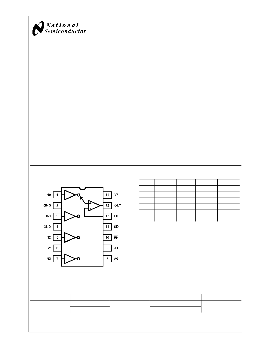
Connection Diagram
14-Pin SOIC
20119705
Top View
Truth Table
A1
A0
EN
SD
OUT
1
1
0
0
CH 3
1
0
0
0
CH2
0
1
0
0
CH1
0
0
0
0
CH 0
X
X
1
0
Disable
X
X
X
1
Shutdown
Ordering Information
Package
Part Number
Package Marking
Transport Media
NSC Drawing
14-Pin SOIC
LMH6574MA
LH6574MA
55 Units/Rail
M14A
LMH6574MAX
2.5k Units Tape and Reel
LMH
TM
is a trademark of National Semiconductor Corporation.
November 2004
LMH6574
4:1
High
Speed
V
ideo
Multiplexer
© 2004 National Semiconductor Corporation
DS201197
www.national.com
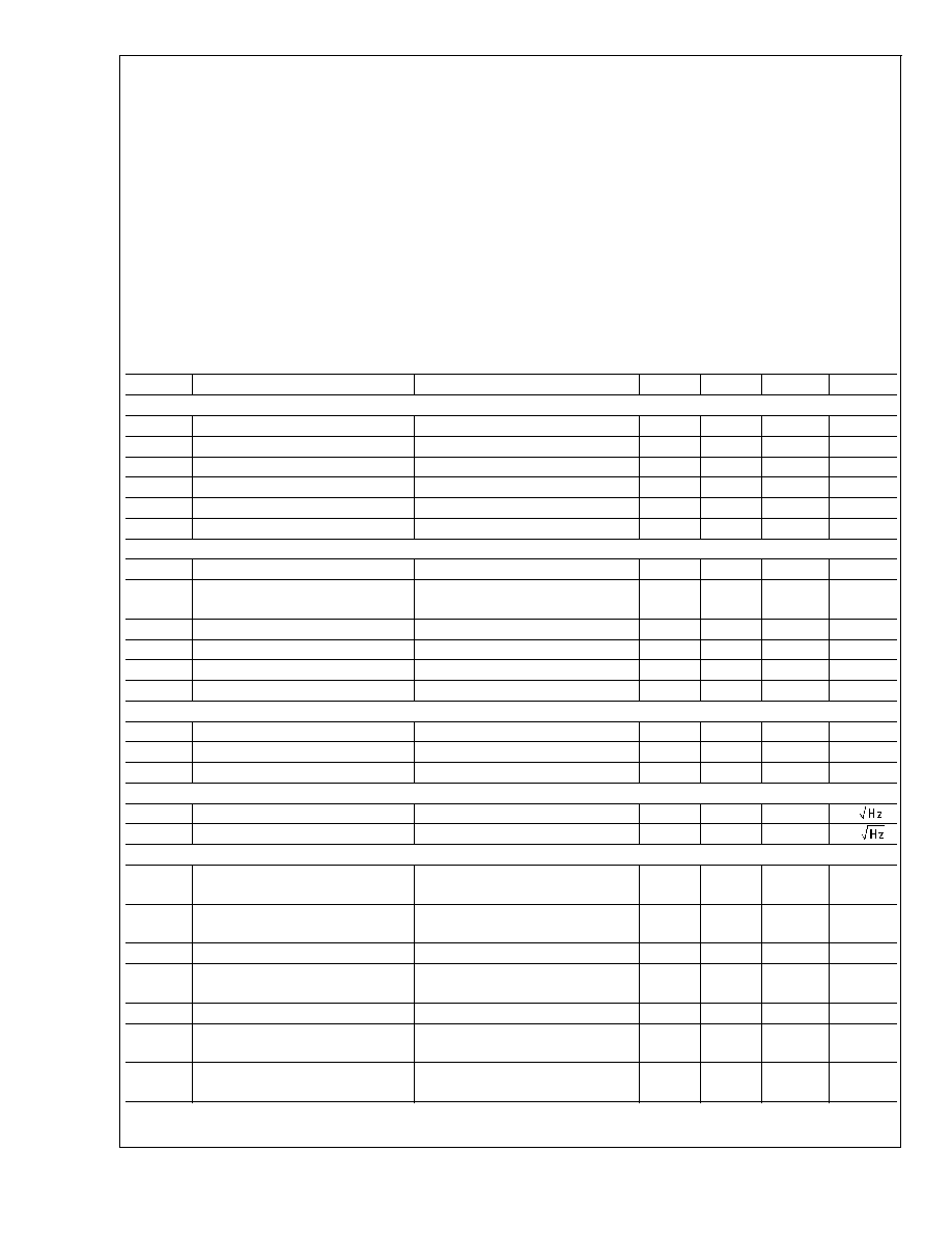
Absolute Maximum Ratings
(Note 1)
If Military/Aerospace specified devices are required,
please contact the National Semiconductor Sales Office/
Distributors for availability and specifications.
ESD Tolerance
(Note 4)
Human Body Model
2000V
Machine Model
200V
Supply Voltage (V
+
- V
-
)
13.2V
I
OUT
(Note 3)
130 mA
Signal & Logic Input Pin Voltage
±
(V
S
+0.6V)
Signal & Logic Input Pin Current
±
20 mA
Maximum Junction Temperature
+150∞C
Storage Temperature Range
-65∞C to +150∞C
Soldering Information
Infrared or Convection (20 sec)
235 ∞C
Wave Soldering (10 sec)
260 ∞C
Operating Ratings
(Note 1)
Operating Temperature
-40 ∞C to 85 ∞C
Supply Voltage Range
6V to 12V
Thermal Resistance
Package
(
JA
)
(
JC
)
14-Pin SOIC
130∞C/W
40∞C/W
±
5V Electrical Characteristics
V
S
=
±
5V, R
L
= 100
, A
V
=2 V/V, T
J
=25 ∞C, Unless otherwise specified. Bold numbers specify limits at temperature extremes.
Symbol
Parameter
Conditions (Note 2)
Min
Typ
Max
Units
Frequency Domain Performance
SSBW
-3 dB Bandwidth
V
OUT
= 0.5V
PP
500
MHz
LSBW
≠3 dB Bandwidth
V
OUT
= 2V
PP
400
MHz
.1 dBBW
0. 1 dB Bandwidth
V
OUT
= 0.25V
PP
150
MHz
DG
Differential Gain
R
L
= 150
, f=4.43 MHz
0.02
%
DP
Differential Phase
R
L
= 150
, f=4.43MHz
0.05
deg
XTLK
Channel to Channel Crosstalk
All Hostile, 5MHz
-85
dB
Time Domain Response
TRS
Channel to Channel Switching Time
Logic transition to 90% output
8
ns
Enable and Disable Times
Logic transition to 90% or 10%
output.
10
ns
TRL
Rise and Fall Time
4V Step
2.4
ns
TSS
Settling Time to 0.05%
2V Step
17
ns
OS
Overshoot
2V Step
5
%
SR
Slew Rate
4V Step
2200
V/µs
Distortion
HD2
2
nd
Harmonic Distortion
2V
PP
, 5 MHz
-68
dBc
HD3
3
rd
Harmonic Distortion
2V
PP
, 5 MHz
-84
dBc
IMD
3
rd
Order Intermodulation Products
10MHz, Two tones 2Vpp at output
-80
dBc
Equivalent Input Noise
VN
Voltage
>
1MHz, Input Referred
5
nV
ICN
Current
>
1MHz, Input Referred
5
pA/
Static, DC Performance
CHGM
Channel to Channel Gain
Difference
DC, Difference in gain between
channels
±
0.005
±
0.032
±
0.035
%
VIO
Input Offset Voltage (Note 5)
V
IN
= 0V
1
±
20
±
25
mV
DVIO
Offset Voltage Drift
30
µV/∞C
IBN
Input Bias Current (Notes 7, 5)
V
IN
= 0V
-3
±
5
±
5.6
µA
DIBN
Bias Current Drift
11
nA/∞C
Inverting Input Bias Current
Pin 12, Feedback point,
V
IN
= 0V
-7
±
10
±
13
PSRR
Power Supply Rejection Ratio
(Note 5)
DC, Input referred
47
45
54
dB
LMH6574
www.national.com
2
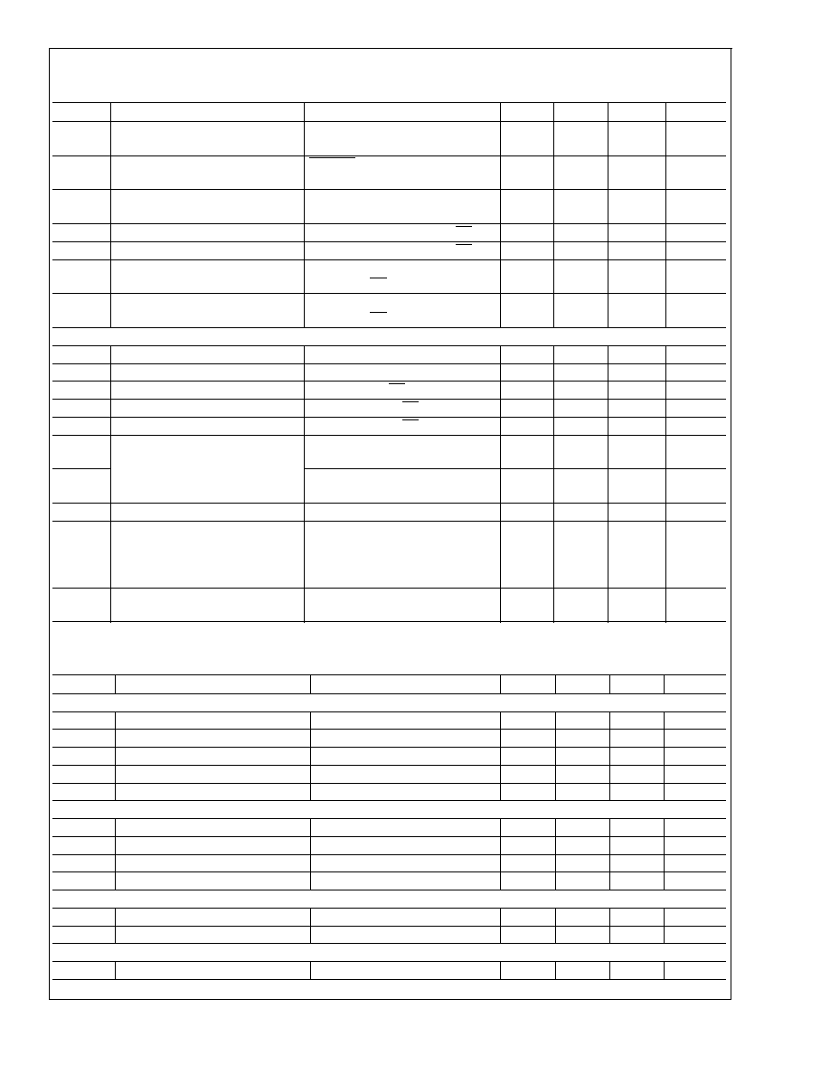
±
5V Electrical Characteristics
(Continued)
V
S
=
±
5V, R
L
= 100
, A
V
=2 V/V, T
J
=25 ∞C, Unless otherwise specified. Bold numbers specify limits at temperature extremes.
Symbol
Parameter
Conditions (Note 2)
Min
Typ
Max
Units
ICC
Supply Current (Note 5)
No Load
13
16
18
mA
Supply Current Disabled(Note 5)
ENABLE
>
2V
4.7
5.8
5.9
mA
Supply Current Shutdown
SHUTDOWN
>
2V
1.8
2.5
2.6
mA
VIH
Logic High Threshold(Note 5)
Select & Enable Pins (SD & EN)
2.0
V
VIL
Logic Low Threshold (Note 5)
Select & Enable Pins (SD & EN)
0.8
V
IiL
Logic Pin Input Current Low (Note
7)
Logic Input = 0V Select & Enable
Pins (SD & EN)
-2.9
-8.5
-1
µA
IiH
Logic Pin Input Current High (Note
7)
Logic Input = 2.0V, Select & Enable
Pins (SD & EN)
47
68
72.5
µA
Miscellaneous Performance
RIN+
Input Resistance
5
k
CIN
Input Capacitance
0.8
pF
ROUT
Output Resistance
Output Active, (EN and SD
<
0.8 V)
0.04
ROUT
Output Resistance
Output Disabled, (EN or SD
>
2V)
3000
COUT
Output Capacitance
Output Disabled, (EN or SD
>
2V)
3.1
pF
VO
Output Voltage Range
No Load
±
3.54
±
3.53
±
3.7
V
VOL
R
L
= 100
±
3.18
±
3.17
±
3.5
V
CMIR
Input Voltage Range
±
2.5
±
2.6
V
IO
Linear Output Current (Notes 5, 7)
V
IN
= 0V,
+60
-70
+50
-60
±
80
mA
ISC
Short Circuit Current(Note 3)
V
IN
=
±
2V, Output shorted to
ground
±
230
mA
±
3.3V Electrical Characteristics
V
S
=
±
3.3V, R
L
= 100
, A
V
=2 V/V; Unless otherwise specified.
Symbol
Parameter
Conditions (Note 2)
Min
Typ
Max
Units
Frequency Domain Performance
SSBW
-3 dB Bandwidth
V
OUT
= 0.5V
PP
475
MHz
LSBW
-3 dB Bandwidth
V
OUT
= 2.0V
PP
375
MHz
0.1 dBBW
0.1 dB Bandwidth
V
OUT
= 0.5V
PP
100
MHz
GFP
Peaking
DC to 200MHz
0.4
dB
XTLK
Channel to Channel Crosstalk
All Hostile, f=5MHz
-85
dBc
Time Domain Response
TRL
Rise and Fall Time
2V Step
2
ns
TSS
Settling Time to 0.05%
2V Step
20
ns
OS
Overshoot
2V Step
5
%
SR
Slew Rate
2V Step
1400
V/µs
Distortion
HD2
2
nd
Harmonic Distortion
2 V
PP
, 10MHz
-67
dBc
HD3
3
rd
Harmonic Distortion
2 V
PP
, 10MHz
-87
dBc
Static, DC Performance
VIO
Input Offset Voltage
V
IN
= 0V
-5
mV
LMH6574
www.national.com
3
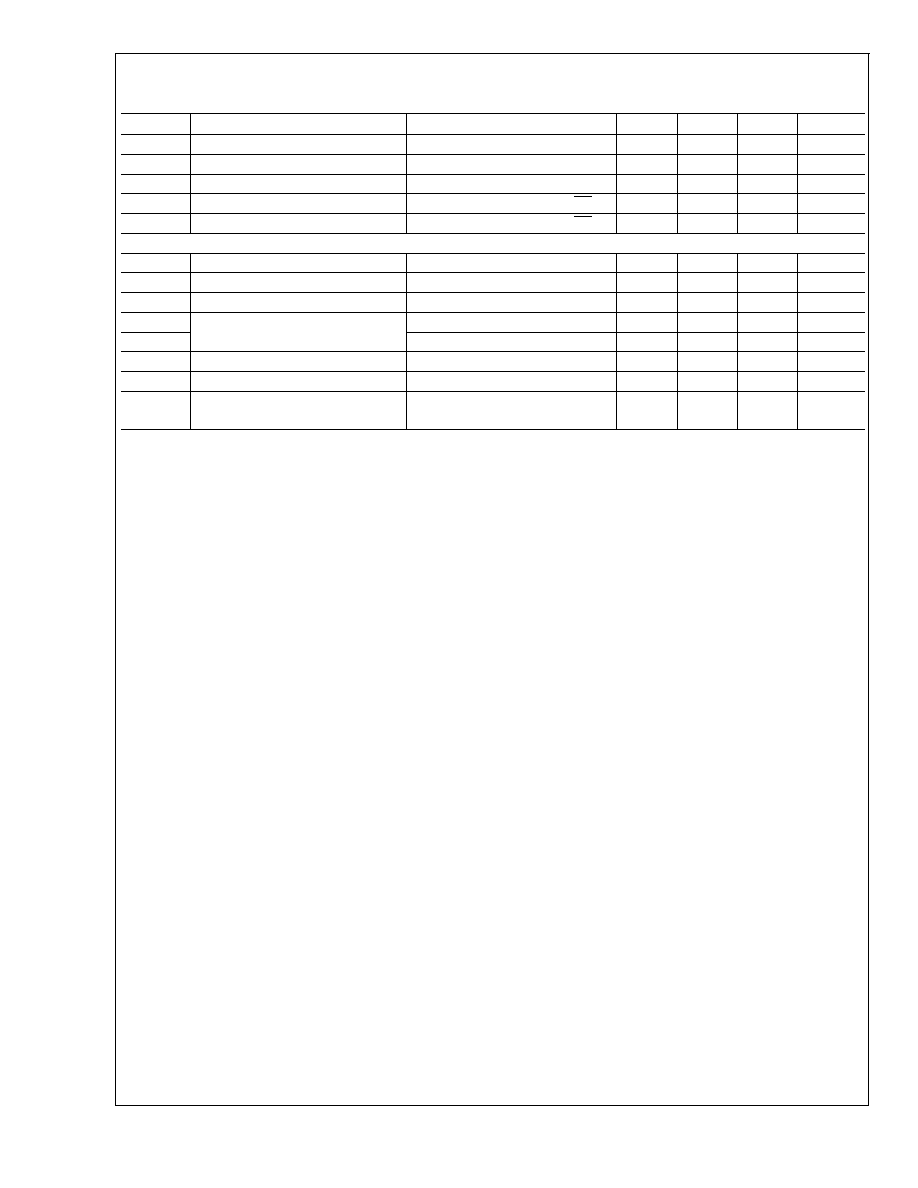
±
3.3V Electrical Characteristics
(Continued)
V
S
=
±
3.3V, R
L
= 100
, A
V
=2 V/V; Unless otherwise specified.
Symbol
Parameter
Conditions (Note 2)
Min
Typ
Max
Units
IBN
Input Bias Current (Note 7)
V
IN
= 0V
-3
µA
PSRR
Power Supply Rejection Ratio
DC, Input Referred
49
dB
ICC
Supply Current
No Load
12
mA
VIH
Logic High Threshold
Select & Enable Pins (SD & EN)
1.3
V
VIL
Logic Low Threshold
Select & Enable Pins (SD & EN)
0.4
V
Miscellaneous Performance
RIN+
Input Resistance
5
k
CIN
Input Capacitance
0.8
pF
ROUT
Output Resistance
0.06
VO
Output Voltage Range
No Load
±
2
V
VOL
R
L
= 100
±
1.8
V
CMIR
Input Voltage Range
±
1.2
V
IO
Linear Output Current
V
IN
= 0V
±
60
mA
ISC
Short Circuit Current
V
IN
=
±
1V, Output shorted to
ground
±
150
mA
Note 1: Absolute Maximum Ratings indicate limits beyond which damage to the device may occur. Operating Ratings indicate conditions for which the device is
intended to be functional, but specific performance is not guaranteed. For guaranteed specifications, see the Electrical Characteristics tables.
Note 2: Electrical Table values apply only for factory testing conditions at the temperature indicated. Factory testing conditions result in very limited self-heating of
the device such that T
J
= T
A
. No guarantee of parametric performance is indicated in the electrical tables under conditions of internal self heating where T
J
>
T
A
.
See Applications Section for information on temperature de-rating of this device. Min/Max ratings are based on product testing, characterization and simulation.
Individual parameters are tested as noted.
Note 3: The maximum output current (I
OUT
) is determined by the device power dissipation limitations (The junction temperature cannot be allowed to exceed
150∞C). See the Power Dissipation section of the Application Section for more details. A short circuit condition should be limited to 5 seconds or less.
Note 4: Human Body model, 1.5k
in series with 100pF. Machine model, 0 In series with 200pF
Note 5: Parameters guaranteed by electrical testing at 25∞C.
Note 6: Parameters guaranteed by design.
Note 7: Positive Value is current into device.
LMH6574
www.national.com
4
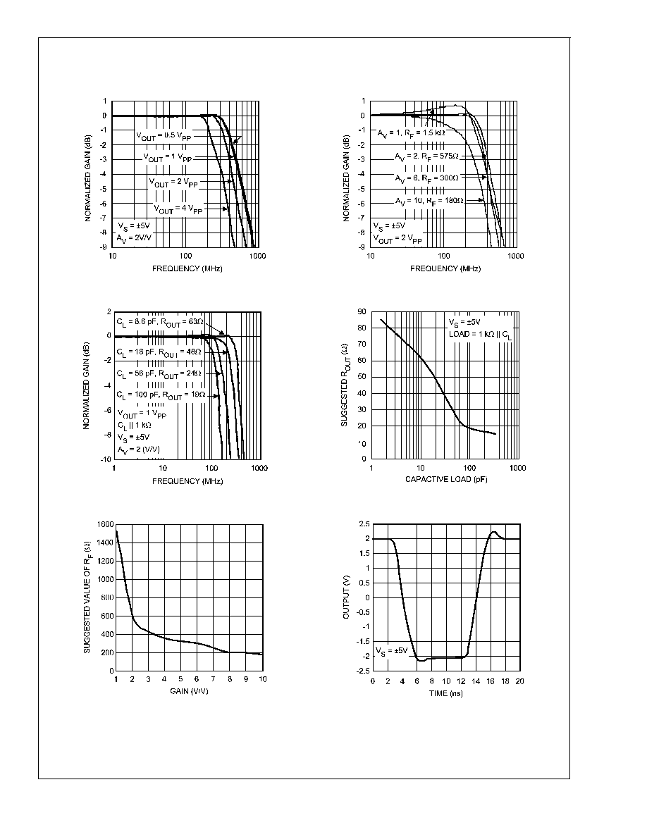
Typical Performance Characteristics
V
s
=
±
5V, R
L
= 100
, A
V
=2, R
F
=R
G
=575
; unless otherwise
specified.
Frequency Response vs. V
OUT
Frequency Response vs. Gain
20119702
20119703
Frequency Response vs. Capacitive Load
Suggested R
OUT
vs. Capacitive Load
20119714
20119715
Suggested Value of R
F
vs. Gain
Pulse Response 4V
PP
20119701
20119725
LMH6574
www.national.com
5