 | ÐлекÑÑоннÑй компоненÑ: LMH6601 | СкаÑаÑÑ:  PDF PDF  ZIP ZIP |
LMH6601 250 MHz, 2.4V CMOS Op Amp with Shutdown
LMH6601
250 MHz, 2.4V CMOS Op Amp with Shutdown
General Description
The LMH6601 is a low voltage (2.4V 5.5V), high speed
voltage feedback operational amplifier suitable for use in a
variety of consumer and industrial applications. With a band-
width of 125 MHz at a gain of +2 and guaranteed high output
current of 100 mA, the LMH6601 is an ideal choice for video
line driver applications including HDTV. Low input bias cur-
rent (50 pA maximum), rail-to-rail output, and low current
noise allow the LMH6601 to be used in various industrial
applications such as transimpedance amplifiers, active fil-
ters, or high-impedance buffers. The LMH6601 is an attrac-
tive solution for systems which require high performance at
low supply voltages. The LMH6601 is available in a 6-pin
SC70 package, and includes a micropower shutdown fea-
ture.
Features
V
S
= 3.3V, T
A
= 25°C, A
V
= 2 V/V, R
L
= 150
to V
-
, unless
specified.
n
125 MHz -3 dB small signal bandwidth
n
75 MHz -3 dB large signal bandwidth
n
30 MHz large signal 0.1 dB gain flatness
n
260 V/µs slew rate
n
0.25%/0.25° differential gain/differential phase
n
Rail-to-rail output
n
2.4V 5.5V single supply operating range
n
SC70-6 Package
Applications
n
Video amplifier
n
Charge amplifier
n
Set-top box
n
Sample & hold
n
Transimpedance amplifier
n
Line driver
n
High impedance buffer
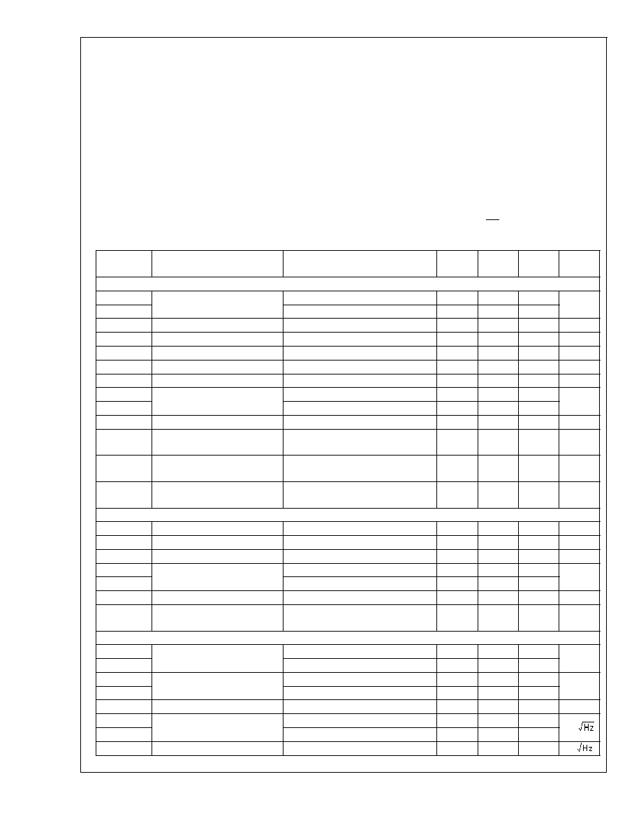
Response at a Gain of +2 for Various Supply Voltages
20136441
June 2006
LMH6601
250
MHz,
2.4V
CMOS
Op
Amp
with
Shutdown
© 2006 National Semiconductor Corporation
DS201364
www.national.com
Absolute Maximum Ratings
(Note 1)
If Military/Aerospace specified devices are required,
please contact the National Semiconductor Sales Office/
Distributors for availability and specifications.
ESD Tolerance (Note 4)
Human Body Model
2 kV
Machine Model
200V
V
IN
Differential
±
2.5V
Input Current
±
10 mA
Output Current
200 mA (Note 3)
Supply Voltage (V
+
V
-
)
6.0V
Voltage at Input/Output Pins
V
+
+0.5V, V
-
-0.5V
Storage Temperature Range
-65°C to +150°C
Junction Temperature
+150°C
Soldering Information
Infrared or Convection (20 sec.)
235°C
Wave Soldering (10 sec.)
260°C
Operating Ratings
(Note 1)
Supply Voltage (V
+
V
-
)
2.4V to 5.5V
Operating Temperature Range
-40°C to +85°C
Package Thermal Resistance (
JA
)
6-pin SC70
414°C/W
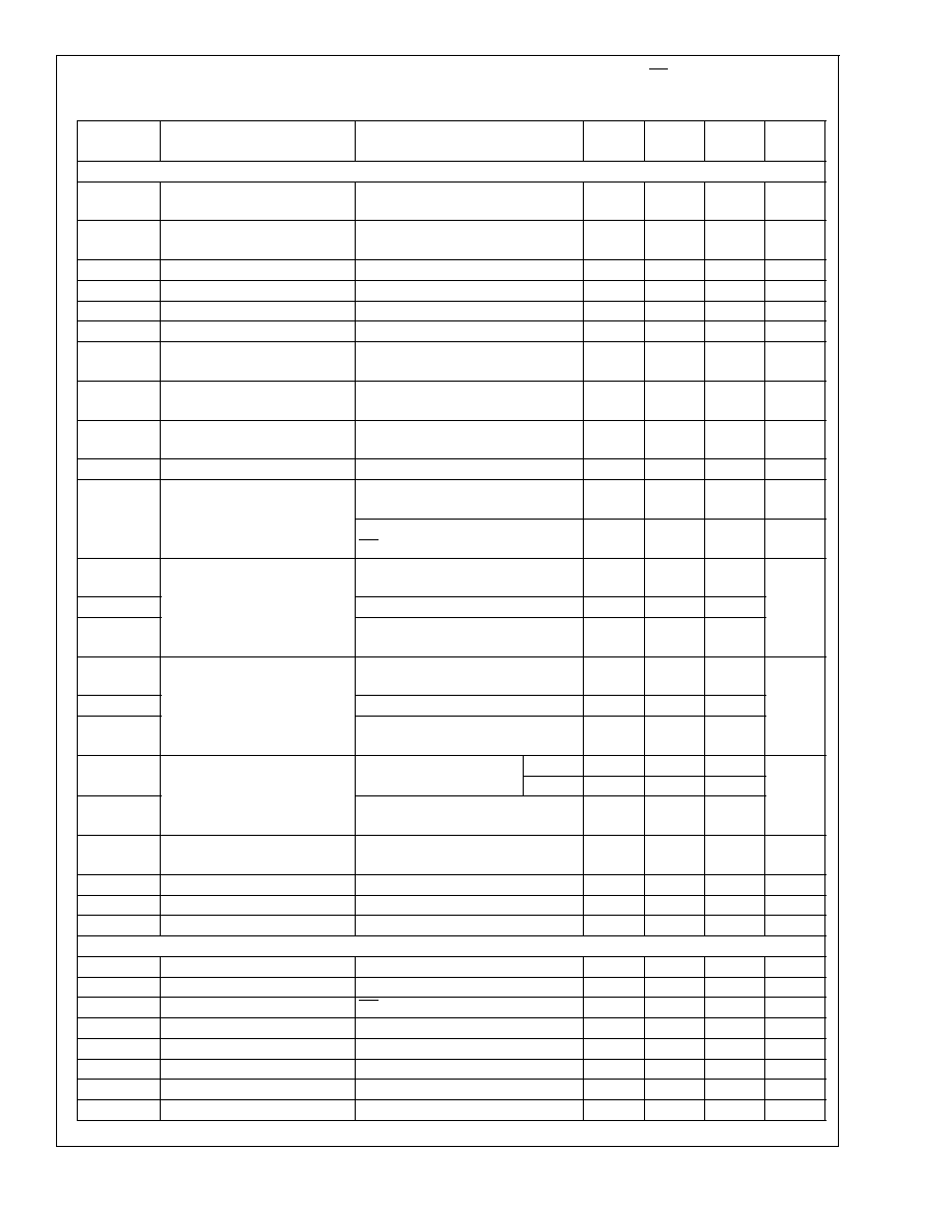
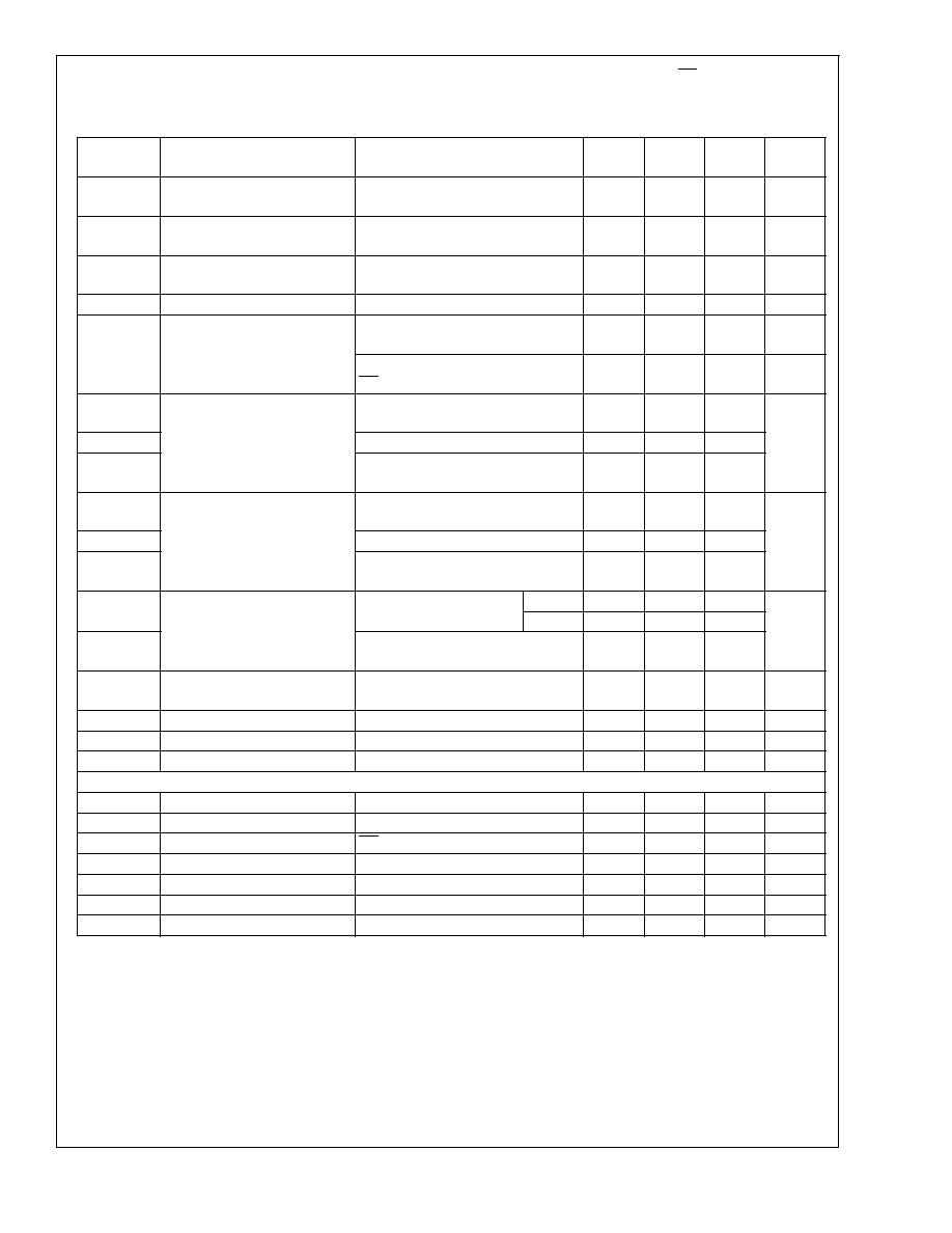
5V Electrical Characteristics
Single Supply with V
S
= 5V, A
V
= +2, R
F
= 604
, SD tied to V
+
, V
OUT
=
V
S
/2, R
L
= 150
to V
-
unless otherwise specified. Boldface limits apply at temperature extremes. (Note 2)
Symbol
Parameter
Condition
Min
(Note 6)
Typ
(Note 6)
Max
(Note 6)
Units
Frequency Domain Response
SSBW
3 dB Bandwidth Small Signal
V
OUT
= 0.25 V
PP
130
MHz
SSBW_1
V
OUT
= 0.25 V
PP
, A
V
= +1
250
Peak
Peaking
V
OUT
= 0.25 V
PP
, A
V
= +1
2.5
dB
Peak_1
Peaking
V
OUT
= 0.25 V
PP
0
dB
LSBW
3 dB Bandwidth Large Signal
V
OUT
= 2 V
PP
81
MHz
Peak_2
Peaking
V
OUT
= 2 V
PP
0
dB
0.1 dB BW
0.1 dB Bandwidth
V
OUT
= 2 V
PP
30
MHz
GBWP_1k
Gain Bandwidth Product
Unity Gain, R
L
= 1 k
to V
S
/2
155
MHz
GBWP_150
Unity Gain, R
L
= 150
to V
S
/2
125
A
VOL
Large Signal Open Loop Gain
0.5V
<
V
OUT
<
4.5V
56
66
dB
PBW
Full Power BW
1 dB, A
V
= +4, V
OUT
= 4.2 V
PP
,
R
L
= 150
to V
S
/2
30
MHz
DG
Differential Gain
4.43 MHz, 1.7V
V
OUT
3.3V,
R
L
= 150
to V
-
0.06
%
DP
Differential Phase
4.43 MHz, 1.7V
V
OUT
3.3V
R
L
= 150
to V
-
0.10
deg
Time Domain Response
TRS/TRL
Rise & Fall Time
0.25V Step
2.6
ns
OS
Overshoot
0.25V Step
10
%
SR
Slew Rate
2V Step
275
V/µs
T
S
Settling Time
1V Step,
±
0.1%
50
ns
T
S_1
1V Step,
±
0.02%
220
PD
Propagation Delay
Input to Output, 250 mV Step, 50%
2.4
ns
C
L
Cap Load Tolerance
A
V
= -1, 10% Overshoot, 75
in
Series
50
pF
Distortion & Noise Performance
HD2
Harmonic Distortion (2
nd
)
2 V
PP
, 10 MHz
-56
dBc
HD2_1
4 V
PP
, 10 MHz, R
L
= 1 k
to V
S
/2
-61
HD3
Harmonic Distortion (3
rd
)
2 V
PP
, 10 MHz
-73
dBc
HD3_1
4 V
PP
, 10 MHz, R
L
= 1 k
to V
S
/2
-64
THD
Total Harmonic Distortion
4 V
PP
, 10 MHz, R
L
= 1 k
to V
S
/2
-58
V
N1
Input Voltage Noise
>
10 MHz
7
nV/
V
N2
1 MHz
10
I
N
Input Current Noise
>
1 MHz
50
fA/
LMH6601
www.national.com
2
5V Electrical Characteristics
Single Supply with V
S
= 5V, A
V
= +2, R
F
= 604
, SD tied to V
+
, V
OUT
= V
S
/2,
R
L
= 150
to V
-
unless otherwise specified. Boldface limits apply at temperature extremes. (Note 2) (Continued)
Symbol
Parameter
Condition
Min
(Note 6)
Typ
(Note 6)
Max
(Note 6)
Units
Static, DC Performance
V
IO
Input Offset Voltage
±
1
±
2.4
±
5.0
mV
DV
IO
Input Offset Voltage Average
Drift
(Note 8)
-5
µV/°C
I
B
Input Bias Current
(Note 9)
5
50
pA
I
OS
Input Offset Current
(Note 9)
2
25
pA
R
IN
Input Resistance
>
100
G
C
IN
Input Capacitance
1.3
pF
+PSRR
Positive Power Supply
Rejection Ratio
DC
55
51
59
dB
-PSRR
Negative Power Supply
Rejection Ratio
DC
53
50
61
dB
CMRR
Common Mode Rejection Ratio DC
56
53
68
dB
CMVR
Input Voltage Range
CMRR
>
50 dB
V
-
-0.20
V
+
- 1.5
V
I
CC
Supply Current
Normal Operation
V
OUT
= V
S
/2
9.6
11.5
13.5
mA
Shutdown
SD tied to
0.5V (Note 5)
100
nA
VOH1
Output High Voltage
(Relative to V
+
)
R
L
= 150
to V
210
480
190
mV
VOH2
R
L
= 75
to V
S
/2
190
VOH3
R
L
= 10 k
to V
60
110
12
VOL1
Output Low Voltage
(Relative to V
)
R
L
= 150
to V
+5
+45
+125
mV
VOL2
R
L
= 75
to V
S
/2
+120
VOL3
R
L
= 10 k
to V
+5
+45
+125
I
O
Output Current
V
OUT
<
0.6V from
Respective Supply
Source
150
mA
Sink
180
I
O
_1
V
OUT
= V
S
/2,
V
ID
=
±
18 mV (Note 10)
±
100
Load
Output Load Rating
THD
<
-30 dBc, f = 200 kHz,
R
L
tied to V
S
/2, V
OUT
= 4 V
PP
20
R
O
_Enabled Output Resistance
Enabled, A
V
= +1
0.2
R
O
_Disabled Output Resistance
Shutdown
>
100
M
C
O
_Disabled Output Capacitance
Shutdown
5.0
pF
Miscellaneous Performance
VDMAX
Voltage Limit for Disable (Pin 5) (Note 5)
0
0.5
V
VDMIN
Voltage Limit for Enable (Pin 5) (Note 5)
4.5
5.0
V
I
i
Logic Input Current (Pin 5)
SD = 5V (Note 5)
10
pA
V
_glitch
Turn-on Glitch
2.2
V
T
on
Turn-on Time
1.4
µs
T
off
Turn-off Time
520
ns
Isolation
OFF
Off Isolation
1 MHz, R
L
= 1 k
60
dB
T_OL
Overload Recovery
<
20
ns
LMH6601
www.national.com
3
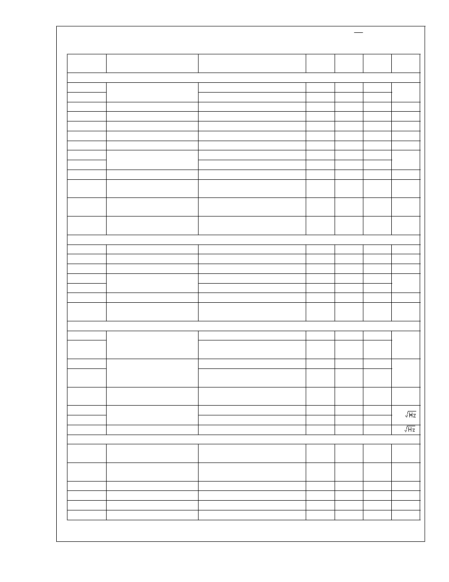
3.3V Electrical Characteristics
Single Supply with V
S
= 3.3V, A
V
= +2, R
F
= 604
, SD tied to V
+
,
V
OUT
= V
S
/2, R
L
= 150
to V
-
unless otherwise specified. Boldface limits apply at temperature extremes. (Note 2)
Symbol
Parameter
Condition
Min
(Note 6)
Typ
(Note 6)
Max
(Note 6)
Units
Frequency Domain Response
SSBW
3 dB Bandwidth Small Signal
V
OUT
= 0.25 V
PP
125
MHz
SSBW_1
V
OUT
= 0.25 V
PP
, A
V
= +1
250
Peak
Peaking
V
OUT
= 0.25 V
PP
, A
V
= +1
3
dB
Peak_1
Peaking
V
OUT
= 0.25 V
PP
0.05
dB
LSBW
3 dB Bandwidth Large Signal
V
OUT
= 2 V
PP
75
MHz
Peak_2
Peaking
V
OUT
= 2 V
PP
0
dB
0.1 dB BW
0.1 dB Bandwidth
V
OUT
= 2 V
PP
30
MHz
GBWP_1k
Gain Bandwidth Product
Unity Gain, R
L
= 1 k
to V
S
/2
115
MHz
GBWP_150
Unity Gain, R
L
= 150
to V
S
/2
105
A
VOL
Large Signal Open Loop Gain
0.3V
<
V
OUT
<
3V
56
67
dB
PBW
Full Power BW
1 dB, A
V
= +4, V
OUT
= 2.8V
PP
,
R
L
= 150
to V
S
/2
30
MHz
DG
Differential Gain
4.43 MHz, 0.85V
V
OUT
2.45V,
R
L
= 150
to V
-
0.0.6
%
DP
Differential Phase
4.43 MHz, 0.85V
V
OUT
2.45V
R
L
= 150
to V
-
0.23
deg
Time Domain Response
TRS/TRL
Rise & Fall Time
0.25V Step
2.7
ns
OS
Overshoot
0.25V Step
10
%
SR
Slew Rate
2V Step
260
V/µs
T
S
Settling Time
1V Step,
±
0.1%
70
ns
T
S_1
1V Step,
±
0.02%
300
PD
Propagation Delay
Input to Output, 250 mV Step, 50%
2.6
ns
C
L
Cap Load Tolerance
A
V
= -1, 10% Overshoot, 82
in
Series
50
pF
Distortion & Noise Performance
HD2
Harmonic Distortion (2
nd
)
2 V
PP
, 10 MHz
-61
dBc
HD2_1
2 V
PP
, 10 MHz
R
L
= 1 k
to V
S
/2
-79
HD3
Harmonic Distortion (3
rd
)
2 V
PP
, 10 MHz
-53
dBc
HD3_2
2 V
PP
, 10 MHz
R
L
= 1 k
to V
S
/2
-69
THD
Total Harmonic Distortion
2 V
PP
, 10 MHz
R
L
= 1 k
to V
S
/2
-66
dBc
V
N1
Input Voltage Noise
>
10 MHz
7
nV/
V
N2
1 MHz
10
I
N
Input Current Noise
>
1 MHz
50
fA/
Static, DC Performance
V
IO
Input Offset Voltage
±
1
±
2.6
±
5.5
mV
DV
IO
Input Offset Voltage Average
Drift
(Note 8)
-4.5
µV/°C
I
B
Input Bias Current
(Note 9)
5
50
pA
I
OS
Input Offset Current
(Note 9)
2
25
pA
R
IN
Input Resistance
>
100
G
C
IN
Input Capacitance
1.4
pF
LMH6601
www.national.com
4
3.3V Electrical Characteristics
Single Supply with V
S
= 3.3V, A
V
= +2, R
F
= 604
, SD tied to V
+
,
V
OUT
= V
S
/2, R
L
= 150
to V
-
unless otherwise specified. Boldface limits apply at temperature extremes. (Note
2) (Continued)
Symbol
Parameter
Condition
Min
(Note 6)
Typ
(Note 6)
Max
(Note 6)
Units
+PSRR
Positive Power Supply
Rejection Ratio
DC
61
51
80
dB
-PSRR
Negative Power Supply
Rejection Ratio
DC
57
52
72
dB
CMRR
Common Mode Rejection Ratio DC
58
55
73
dB
CMVR
Input Voltage Range
CMRR
>
50 dB
V
-
-0.20
V
+
-1.5
V
I
CC
Supply Current
Normal Operation
V
OUT
= V
S
/2
9.2
11
13
mA
Shutdown
SD tied to
0.33V (Note 5)
100
nA
VOH1
Output High Voltage
(Relative to V
+
)
R
L
= 150
to V
210
360
190
mV
VOH2
R
L
= 75
to V
S
/2
190
VOH3
R
L
= 10 k
to V
-
50
100
10
VOL1
Output Low Voltage
(Relative to V
)
R
L
= 150
to V
+4
+45
+125
mV
VOL2
R
L
= 75
to V
S
/2
+105
VOL3
R
L
= 10 k
to V
+4
+45
+125
I
O
Output Current
V
OUT
<
0.6V from
Respective Supply
Source
50
mA
Sink
75
I
O
_1
V
OUT
= V
S
/2, V
ID
=
±
18 mV
(Note 10)
±
75
Load
Output Load Rating
THD
<
-30 dBc, f = 200 kHz,
R
L
tied to V
S
/2, V
OUT
= 2.6 V
PP
25
R
O
_Enabled Output Resistance
Enabled, A
V
= +1
0.2
R
O
_Disabled Output Resistance
Shutdown
>
100
M
C
O
_Disabled Output Capacitance
Shutdown
5.6
pF
Miscellaneous Performance
VDMAX
Voltage Limit for Disable (Pin 5) (Note 5)
0
0.33
V
VDMIN
Voltage Limit for Enable (Pin 5) (Note 5)
2.97
3.3
V
I
i
Logic Input Current (Pin 5)
SD = 3.3V (Note 5)
8
pA
V
_glitch
Turn-on Glitch
1.6
V
T
on
Turn-on Time
3.5
µs
T
off
Turn-off Time
500
ns
Isolation
OFF
Off Isolation
1 MHz, R
L
= 1 k
60
dB
LMH6601
www.national.com
5
Document Outline