 | –≠–ª–µ–∫—Ç—Ä–æ–Ω–Ω—ã–π –∫–æ–º–ø–æ–Ω–µ–Ω—Ç: LMH6609 | –°–∫–∞—á–∞—Ç—å:  PDF PDF  ZIP ZIP |
LMH6609
900MHz Voltage Feedback Op Amp
General Description
The LMH6609 is an ultra wideband, unity gain stable, low
power, voltage feedback op amp that offers 900MHz band-
width at a gain of 1, 1400V/µs slew rate and 90mA of linear
output current.
The LMH6609 is designed with voltage feedback architec-
ture for maximum flexibility especially for active filters and
integrators. The LMH6609 has balanced, symmetrical inputs
with well-matched bias currents and minimal offset voltage.
With Differential Gain of .01 and Differential Phase of .026
the LMH6609 is suited for video applications. The 90mA of
linear output current makes the LMH6609 suitable for mul-
tiple video loads and cable driving applications as well.
The recommended supply voltage range of 6V to 12V and is
specified at 6.6 and 10V. A low supply current of 7mA (at 10V
supply) makes the LMH6609 useful in a wide variety of
platforms, including portable or remote equipment that must
run from battery power.
The LMH6609 is available in the industry standard 8-pin
SOIC package and in the space-saving 5-pin SOT package.
The LMH6609 is specified for operation over the -40∞C to
+85∞C temperature range. The LMH6609 is manufactured in
National Semiconductor's state-of-the-art VIP10
TM
technol-
ogy for high performance.
Features
n
900MHz -3dB bandwidth (A
V
= 1)
n
Large signal bandwidth and slew rate 100% tested
n
280MHz -3dB bandwidth (A
V
= +2, V
OUT
= 2V
PP
)
n
90mA linear output current
n
1400V/µs slew rate
n
Unity gain stable
n
<
1mV input Offset voltage
n
7mA Supply current (no load)
n
6V to 12V supply voltage range
n
.01/ .026 differential gain/phase PAL
n
3.1nV/
voltage noise
n
Improved replacement for CLC440, 420, 426
Applications
n
Test equipment
n
IF/RF amplifier
n
A/D Input driver
n
Active filter
n
Integrator
n
DAC output buffer
n
Transimpedance amplifier
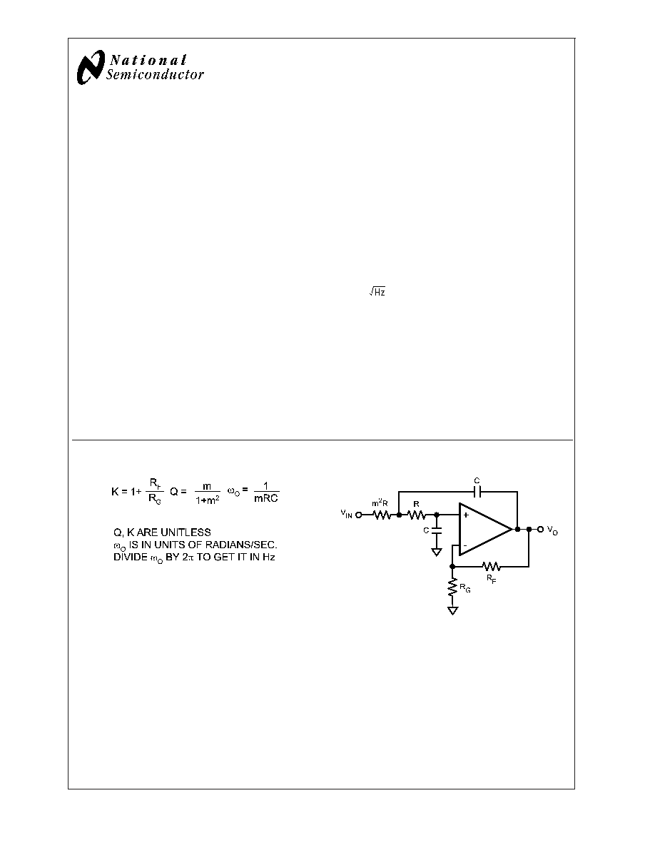
Typical Application
20079037
20079038
Sallen Key Low Pass Filter
August 2003
LMH6609
900MHz
V
oltage
Feedback
Op
Amp
© 2003 National Semiconductor Corporation
DS200790
www.national.com
Absolute Maximum Ratings
(Note 1)
If Military/Aerospace specified devices are required,
please contact the National Semiconductor Sales Office/
Distributors for availability and specifications.
V
S
(V
+
- V
-
)
±
6.6V
I
OUT
(Note 3)
Common Mode Input Voltage
V+ to V-
Maximum Junction Temperature
+150∞C
Storage Temperature Range
-65∞C to +150∞C
Lead Temperature Range
+300∞C
ESD Tolerance (Note 4)
Human Body Model
2000V
Machine Model
200V
Operating Ratings
(Note 3)
Thermal Resistance
Package
(
JC
)
(
JA
)
8-Pin SOIC
65∞C/W
145∞C/W
5-Pin SOT23
120∞C/W
187∞C/W
Operating Temperature
-40∞C
+85∞C
Nominal Supply Voltage
(Note 6)
±
3.3V
±
6V
±
5V Electrical Characteristics
Unless specified, A
V
= +2, R
F
= 250
: V
S
=
±
5V, R
L
= 100
; unless otherwise specified. Boldface limits apply over tempera-
ture Range. (Note 2)
Symbol
Parameter
Conditions
Min
Typ
Max
Units
Frequency Domain Response
SSBW
-3dB Bandwidth
V
OUT
= 0.5V
PP
260
MHz
LSBW
-3dB Bandwidth
V
OUT
= 4.0V
PP
150
170
MHz
SSBWG1
-3dB Bandwidth A
V
= 1
V
OUT
= 0.25V
PP
900
MHz
GFP
.1dB Bandwidth
Gain is Flat to .1dB
130
MHz
DG
Differential Gain
R
L
= 150
, 4.43MHz
0.01
%
DP
Differential Phase
R
L
= 150
, 4.43MHz
0.026
deg
Time Domain Response
TRS
Rise and Fall Time
1V Step
1.6
ns
TRL
4V Step
2.6
ns
t
s
Settling Time to 0.05%
2V Step
15
ns
SR
Slew Rate
4V Step (Note 5)
1200
1400
V/µs
Distortion and Noise Response
HD2
2
nd
Harmonic Distortion
2V
PP
, 20MHz
-63
dBc
HD3
3
rd
Harmonic Distortion
2V
PP
, 20MHz
-57
dBc
Equivalent Input Noise
VN
Voltage Noise
>
1MHz
3.1
nV/
CN
Current Noise
>
1MHz
1.6
pA/
Static, DC Performance
V
IO
Input Offset Voltage
±
0.8
±
2.5
±
3.5
mV
I
BN
Input Bias Current
-2
±
5
±
8
µA
I
BI
Input Offset Current
.1
±
1.5
±
3
µA
PSRR
Power Supply Rejection Ratio
DC, 1V Step
67
65
73
dB
CMRR
Common Mode Rejection Ratio
DC, 2V Step
67
65
73
dB
I
CC
Supply Current
R
L
=
7.0
7.8
8.5
mA
Miscellaneous Performance
R
IN
Input Resistance
1
M
C
IN
Input Capacitance
1.2
pF
R
OUT
Output Resistance
Closed Loop
0.3
LMH6609
www.national.com
2
±
5V Electrical Characteristics
(Continued)
Unless specified, A
V
= +2, R
F
= 250
: V
S
=
±
5V, R
L
= 100
; unless otherwise specified. Boldface limits apply over tempera-
ture Range. (Note 2)
Symbol
Parameter
Conditions
Min
Typ
Max
Units
V
O
Output Voltage Range
R
L
=
±
3.6
±
3.3
±
3.9
V
V
OL
R
L
= 100
±
3.2
±
3.0
±
3.5
V
CMIR
Input Voltage Range
Common Mode, CMRR
>
60dB
±
2.8
±
2.5
±
3.0
V
I
O
Linear Output Current
V
OUT
±
60
±
50
±
90
mA
±
3.3V Electrical Characteristics
Unless specified, A
V
= +2, R
F
= 250
: V
S
=
±
3.3V, R
L
= 100
; unless otherwise specified. Boldface limits apply over tem-
perature Range. (Note 2)
Symbol
Parameter
Conditions
Min
Typ
Max
Units
Frequency Domain Response
SSBW
-3dB Bandwidth
V
OUT
= 0.5V
PP
180
MHz
LSBW
-3dB Bandwidth
V
OUT
= 3.0V
PP
110
MHz
SSBWG1
-3dB Bandwidth A
V
= 1
V
OUT
= 0.25V
PP
450
MHz
GFP
.1dB Bandwidth
V
OUT
= 1V
PP
40
MHz
DG
Differential Gain
R
L
= 150
, 4.43MHz
.01
%
DP
Differential Phase
R
L
= 150
, 4.43MHz
.06
deg
Time Domain Response
TRL
1V Step
2.2
ns
SR
Slew Rate
2V Step (Note 5)
800
V/µs
Distortion and Noise Response
HD2
2
nd
Harmonic Distortion
2V
PP
, 20MHz
-63
dBc
HD3
3
rd
Harmonic Distortion
2V
PP
, 20MHz
-43
dBc
Equivalent Input Noise
VN
Voltage Noise
>
1MHz
3.7
nV/
CN
Current Noise
>
1MHz
1.1
pA/
Static, DC Performance
V
IO
Input Offset Voltage
0.8
±
2.5
±
3.5
mV
I
BN
Input Bias Current
-1
±
3
±
6
µA
I
BI
Input Offset Current
0
±
1.5
±
3
µA
PSRR
Power Supply Rejection Ratio
DC, .5V Step
67
73
dB
CMRR
Common Mode Rejection Ratio
DC, 1V Step
67
75
dB
I
CC
Supply Current
R
L
=
3.6
5
6
mA
Miscellaneous Performance
R
OUT
Input Resistance
Close Loop
.05
V
O
Output Voltage Range
R
L
=
±
2.1
±
2.3
V
V
OL
R
L
= 100
±
1.9
±
2.0
V
CMIR
Input Voltage Range
Common Mode
±
1.3
V
I
O
Linear Output Current
V
OUT
±
30
±
45
mA
LMH6609
www.national.com
3
±
3.3V Electrical Characteristics
(Continued)
Note 1: Absolute Maximum Ratings indicate limits beyond which damage to the device may occur. Operating Ratings indicate conditions for which the device is
intended to be functional, but specific performance is not guaranteed. For guaranteed specifications, see the Electrical Characteristics tables.
Note 2: Electrical Table values apply only for factory testing conditions at the temperature indicated. Factory testing conditions result in very limited self-heating of
the device such that T
J
= T
A
. No guarantee of parametric performance is indicated in the electrical tables under conditions of internal self heating where T
J
>
T
A
.
See Applications Section for information on temperature derating of this device. Min/Max ratings are based on product characterization and simulation. Individual
parameters are tested as noted.
Note 3: The maximum output current (I
OUT
) is determined by device power dissipation limitations. See the Power Dissipation section of the Application Section for
more details.
Note 4: Human body model, 1.5k
in series with 100pF. Machine model, 0 In series with 200pF.
Note 5: rate is Average of Rising and Falling 40-60% slew rates.
Note 6: Nominal Supply voltage range is for supplies with regulation of 10% or better.
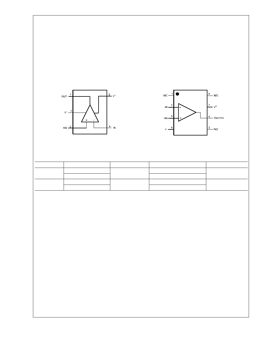
Connection Diagrams
5-Pin SOT23
8-Pin SOIC
20079039
Top View
20079040
Top View
Ordering Information
Package
Part Number
Package Marking
Transport Media
NSC Drawing
8-Pin SOIC
LMH6609MA
LMH6609MA
95 Units/Rails
M08A
LMH6609MAX
2.5k Units Tape and Reel
5-SOT23
LMH6609MF
A89A
1k Units Tape and Reel
MF05A
LMH6609MFX
2.5k Units Tape and Reel
LMH6609
www.national.com
4

Typical Performance Characteristics
Small Signal Non-Inverting Frequency Response
Large Signal Non-Inverting Frequency Response
20079004
20079003
Small Signal Inverting Frequency Response
Large Signal Inverting Frequency Response
20079002
20079010
Frequency Response vs. V
OUT
A
V
= 2
Frequency Response vs. V
OUT
A
V
= 2
20079009
20079001
LMH6609
www.national.com
5