 | ÐлекÑÑоннÑй компоненÑ: LMH6640 | СкаÑаÑÑ:  PDF PDF  ZIP ZIP |
Äîêóìåíòàöèÿ è îïèñàíèÿ www.docs.chipfind.ru
LMH6640
TFT-LCD Single, 16V Rail-to-Rail High Output
Operational Amplifier
General Description
The LMH
TM
6640 is a voltage feedback operational amplifier
with a rail-to-rail output drive capability of 100 mA. Employ-
ing National's patented VIP10 process, the LMH6640 deliv-
ers a bandwidth of 190 MHz at a current consumption of only
4mA. An input common mode voltage range extending to
0.3V below the V- and to within 0.9V of V
+
, makes the
LMH6640 a true single supply op-amp. The output voltage
range extends to within 100 mV of either supply rail providing
the user with a dynamic range that is especially desirable in
low voltage applications.
The LMH6640 offers a slew rate of 170 V/µs resulting in a full
power bandwidth of approximately 28 MHz with 5V single
supply (2 V
PP
, -1 dB). Careful attention has been paid to
ensure device stability under all operating voltages and
modes. The result is a very well behaved frequency re-
sponse characteristic for any gain setting including +1, and
excellent specifications for driving video cables including
total harmonic distortion of -64 dBc
@
5 MHz, differential
gain of 0.12% and differential phase of 0.12°.
Features
(V
S
= 16V, R
L
= 2 k
to V
+
/2, 25°C, Typical Values Unless
Specified)
n
Supply current (no load)
4 mA
n
Output resistance (closed loop 1 MHz)
0.35
n
-3 dB BW (A
V
= 1)
190 MHz
n
Settling time (
±
0.1%, 2 V
PP
)
35 ns
n
Input common mode voltage
-0.3V to 15.1V
n
Output voltage swing
100 mV from rails
n
Linear output current
±
100 mA
n
Total harmonic distortion (2 V
PP
, 5 MHz)
-64 dBc
n
Fully characterized for:
5V & 16V
n
No output phase reversal with CMVR exceeded
n
Differential gain (R
L
= 150
)
0.12%
n
Differential phase (R
L
= 150
)
0.12°
Applications
n
TFT panel V
COM
buffer amplifier
n
Active filters
n
CD/DVD ROM
n
ADC buffer amplifier
n
Portable video
n
Current sense buffer
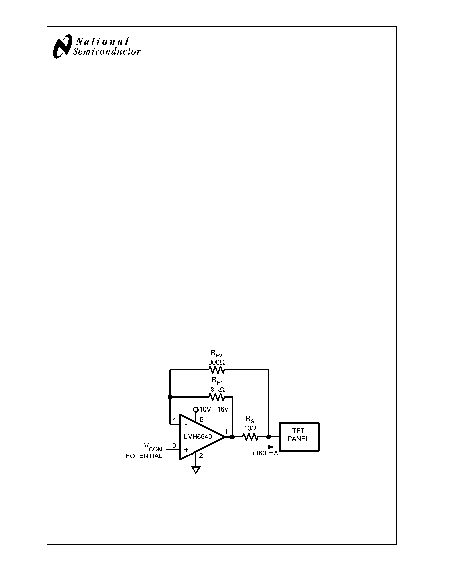
Typical Application
20086234
Typical Application as a TFT Panel V
COM
Driver
LMH
TM
is a trademark of National Semiconductor Corporation.
November 2004
LMH6640
TFT
-LCD
Single,
16V
Rail-to-Rail
High
Output
Operational
Amplifier
© 2004 National Semiconductor Corporation
DS200862
www.national.com
Absolute Maximum Ratings
(Note 1)
If Military/Aerospace specified devices are required,
please contact the National Semiconductor Sales Office/
Distributors for availability and specifications.
ESD Tolerance (Note 2)
Human Body Model
2 KV
Machine Model
200V
V
IN
Differential
±
2.5V
Input Current
±
10 mA
Supply Voltages (V
+
V
-
)
18V
Voltage at Input/Output Pins
V
+
+0.8V, V
-
-0.8V
Storage Temperature Range
-65°C to +150°C
Junction Temperature (Note 4)
+150°C
Soldering Information
Infrared or Convection (20 sec.)
235°C
Wave Soldering (10 sec.)
260°C
Operating Ratings
(Note 3)
Supply Voltage (V
+
V
-
)
4.5V to 16V
Operating Temperature Range
(Note 4)
-40°C to +85°C
Package Thermal Resistance (Note 4)
5-Pin SOT23
265°C/W
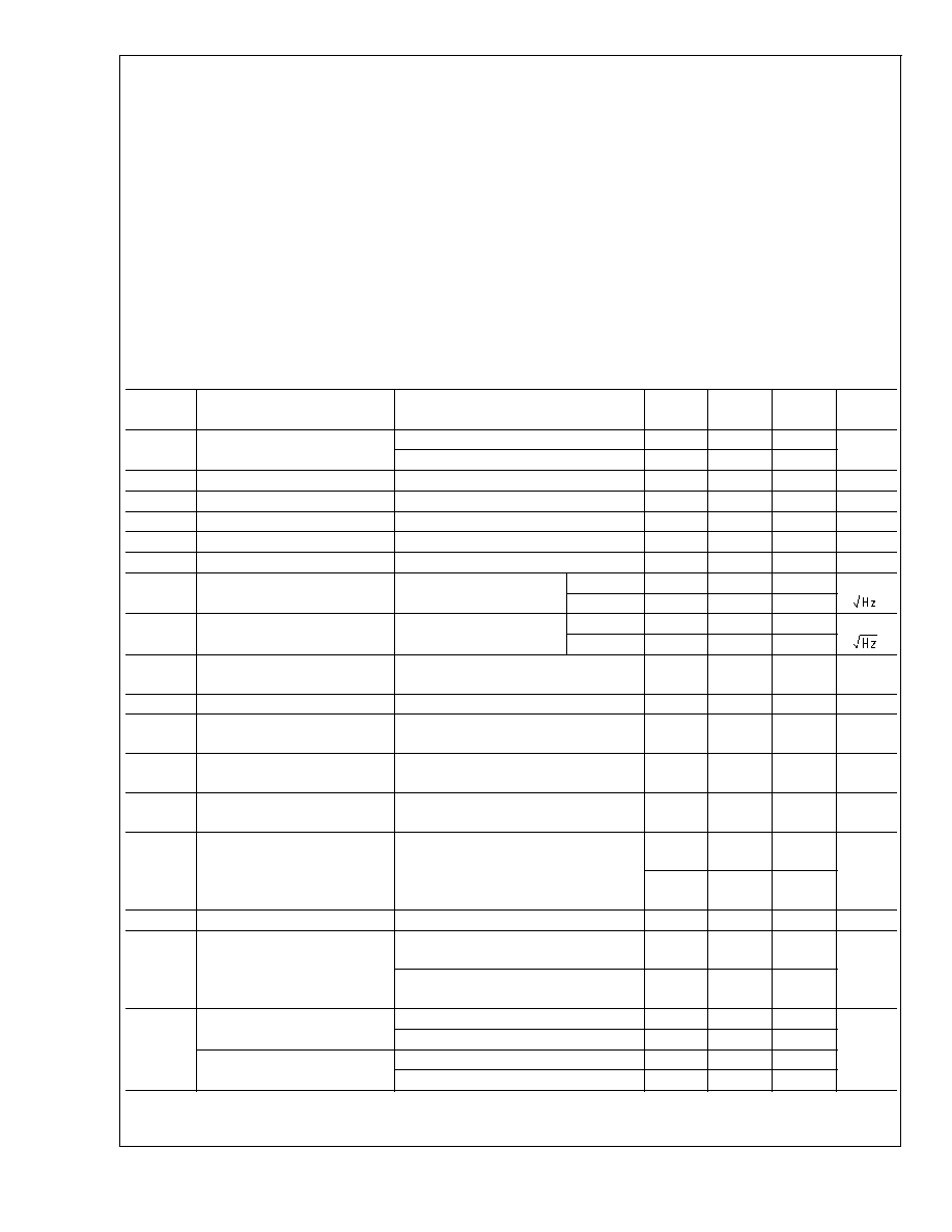
5V Electrical Characteristics
Unless otherwise specified, All limits guaranteed for T
J
= 25°C, V
+
= 5V, V
-
= 0V, V
O
= V
CM
= V
+
/2 and R
L
= 2 k
to V
+
/2.
Boldface limits apply at temperature extremes. (Note 9)
Symbol
Parameter
Conditions
Min
(Note 6)
Typ
(Note 5)
Max
(Note 6)
Units
BW
-3 dB Bandwidth
A
V
= +1 (R
L
= 100
)
150
MHz
A
V
= -1 (R
L
= 100
)
58
BW
0.1 dB
0.1 dB Gain Flatness
A
V
= -3
18
MHz
FPBW
Full Power Bandwidth
A
V
= +1, V
OUT
= 2 V
PP
, -1 dB
28
MHz
LSBW
-3 dB Bandwidth
A
V
= +1, V
O
= 2 V
PP
(R
L
= 100
)
32
MHz
GBW
Gain Bandwidth Product
A
V
= +1, (R
L
= 100
)
59
MHz
SR
Slew Rate (Note 8)
A
V
= -1
170
V/µs
e
n
Input Referred Voltage Noise
f = 10 kHz
23
nV/
f = 1 MHz
15
i
n
Input Referred Current Noise
f = 10 kHz
1.1
pA/
f = 1 MHz
0.7
THD
Total Harmonic Distortion
f = 5 MHz, V
O
= 2 V
PP
, A
V
= +2
R
L
= 1 k
to V
+
/2
65
dBc
t
s
Settling Time
V
O
= 2 V
PP
,
±
0.1%, A
V
= -1
35
ns
V
OS
Input Offset Voltage
1
5
7
mV
I
B
Input Bias Current (Note 7)
-1.2
-2.6
-3.25
µA
I
OS
Input Offset Current
34
800
1400
nA
CMVR
Common Mode Input Voltage
Range
CMRR
50 dB
0.3
0.2
0.1
V
4.0
3.6
4.1
CMRR
Common Mode Rejection Ratio
V
-
V
CM
V
+
-1.5V
72
90
dB
A
VOL
Large Signal Voltage Gain
V
O
= 4 V
PP
, R
L
= 2 k
to V
+
/2
86
82
95
dB
V
O
= 3.75 V
PP
, R
L
= 150
to V
+
/2
74
70
78
V
O
Output Swing High
R
L
= 2 k
to V
+
/2
4.90
4.94
V
R
L
= 150
to V
+
/2
4.75
4.80
Output Swing Low
R
L
= 2 k
to V
+
/2
0.06
0.10
R
L
= 150
to V
+
/2
0.20
0.25
LMH6640
www.national.com
2
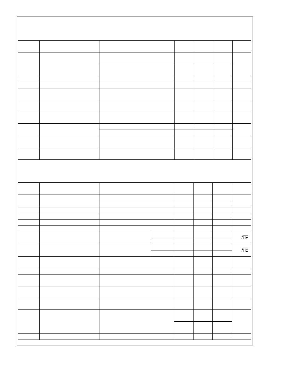
5V Electrical Characteristics
(Continued)
Unless otherwise specified, All limits guaranteed for T
J
= 25°C, V
+
= 5V, V
-
= 0V, V
O
= V
CM
= V
+
/2 and R
L
= 2 k
to V
+
/2.
Boldface limits apply at temperature extremes. (Note 9)
Symbol
Parameter
Conditions
Min
(Note 6)
Typ
(Note 5)
Max
(Note 6)
Units
I
SC
Output Short Circuit Current
(Note 3)
Sourcing to V
+
/2
100
75
130
mA
Sinking from V
+
/2
100
70
130
I
OUT
Output Current
V
O
= 0.5V from either Supply
+75/-90
mA
PSRR
Power Supply Rejection Ratio
4V
V
+
6V
72
80
dB
I
S
Supply Current
No Load
3.7
5.5
8.0
mA
R
IN
Common Mode Input
Resistance
A
V
= +1, f = 1 kHz, R
S
= 1 M
15
M
C
IN
Common Mode Input
Capacitance
A
V
= +1, R
S
= 100 k
1.7
pF
R
OUT
Output Resistance Closed Loop
R
F
= 10 k
, f = 1 kHz, A
V
= -1
0.1
R
F
= 10 k
, f = 1 MHz, A
V
= -1
0.4
DG
Differential Gain
NTSC, A
V
= +2
R
L
= 150
to V
+
/2
0.13
%
DP
Differential Phase
NTSC, A
V
= +2
R
L
= 150
to V
+
/2
0.10
deg
16V Electrical Characteristics
Unless otherwise specified, All limits guaranteed for T
J
= 25°C, V
+
= 16V, V
-
= 0V, V
O
= V
CM
= V
+
/2 and R
L
= 2 k
to V
+
/2.
Boldface limits apply at temperature extremes. (Note 9)
Symbol
Parameter
Conditions
Min
(Note 6)
Typ
(Note 5)
Max
(Note 6)
Units
BW
-3 dB Bandwidth
A
V
= +1 (R
L
= 100
)
190
MHz
A
V
= -1 (R
L
= 100
)
60
BW
0.1 dB
0.1 dB Gain Flatness
A
V
= -2.7
20
MHz
LSBW
-3 dB Bandwidth
A
V
= +1, V
O
= 2 V
PP
(R
L
= 100
)
35
MHz
GBW
Gain Bandwidth Product
A
V
= +1, (R
L
= 100
)
62
MHz
SR
Slew Rate (Note 8)
A
V
= -1
170
V/µs
e
n
Input Referred Voltage Noise
f = 10 kHz
23
nV/
f = 1 MHz
15
i
n
Input Referred Current Noise
f = 10 kHz
1.1
pA/
f = 1 MHz
0.7
THD
Total Harmonic Distortion
f = 5 MHz, V
O
= 2 V
PP
, A
V
= +2
R
L
= 1 k
to V
+
/2
64
dBc
t
s
Settling Time
V
O
= 2 V
PP
,
±
0.1%, A
V
= -1
35
ns
V
OS
Input Offset Voltage
1
5
7
mV
I
B
Input Bias Current (Note 7)
-1
-2.6
-3.5
µA
I
OS
Input Offset Current
34
800
1800
nA
CMVR
Common Mode Input Voltage
Range
CMRR
50 dB
0.3
-0.2
-0.1
V
15.0
14.6
15.1
CMRR
Common Mode Rejection Ratio
V
-
V
CM
V
+
-1.5V
72
90
dB
LMH6640
www.national.com
3
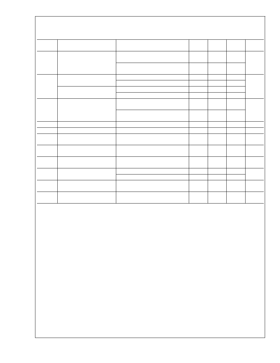
16V Electrical Characteristics
(Continued)
Unless otherwise specified, All limits guaranteed for T
J
= 25°C, V
+
= 16V, V
-
= 0V, V
O
= V
CM
= V
+
/2 and R
L
= 2 k
to V
+
/2.
Boldface limits apply at temperature extremes. (Note 9)
Symbol
Parameter
Conditions
Min
(Note 6)
Typ
(Note 5)
Max
(Note 6)
Units
A
VOL
Large Signal Voltage Gain
V
O
= 15 V
PP
, R
L
= 2 k
to V
+
/2
86
82
95
dB
V
O
= 14 V
PP
, R
L
= 150
to V
+
/2
74
70
78
V
O
Output Swing High
R
L
= 2 k
to V
+
/2
15.85
15.90
V
R
L
= 150
to V
+
/2
15.45
15.78
Output Swing Low
R
L
= 2 k
to V
+
/2
0.10
0.15
R
L
= 150
to V
+
/2
0.21
0.55
I
SC
Output Short Circuit Current
(Note 3)
Sourcing to V
+
/2
60
30
95
mA
Sinking from V
+
/2
50
15
75
I
OUT
Output Current
V
O
= 0.5V from either Supply
±
100
mA
PSRR
Power Supply Rejection Ratio
15V
V
+
17V
72
80
dB
I
S
Supply Current
No Load
4
6.5
7.8
mA
R
IN
Common Mode Input
Resistance
A
V
= +1, f = 1 kHz, R
S
= 1 M
32
M
C
IN
Common Mode Input
Capacitance
A
V
= +1, R
S
= 100 k
1.7
pF
R
OUT
Output Resistance Closed Loop R
F
= 10 k
, f = 1 kHz, A
V
= -1
0.1
R
F
= 10 k
, f = 1 MHz, A
V
= -1
0.3
DG
Differential Gain
NTSC, A
V
= +2
R
L
= 150
to V
+
/2
0.12
%
DP
Differential Phase
NTSC, A
V
= +2
R
L
= 150
to V
+
/2
0.12
deg
Note 1: Absolute maximum Ratings indicate limits beyond which damage to the device may occur. Operating Ratings indicate conditions for which the device is
intended to be functional, but specific performance is not guaranteed. For guaranteed specifications and the test conditions, see the Electrical Characteristics.
Note 2: Human body model, 1.5 k
in series with 100 pF. Machine Model, 0 in series with 200 pF.
Note 3: Applies to both single-supply and split-supply operation. Continuous short circuit operation at elevated ambient temperature can result in exceeding the
maximum allowed junction temperature of 150 °C Short circuit test is a momentary test. Output short circuit duration is infinite for V
S
<
6V at room temperature and
below. For V
S
>
6V, allowable short circuit duration is 1.5 ms.
Note 4: The maximum power dissipation is a function of T
J(MAX)
,
JA
, and T
A
. The maximum allowable power dissipation at any ambient temperature is
P
D
= (T
J(MAX)
-T
A
) /
JA
. All numbers apply for packages soldered directly onto a PC board.
Note 5: Typical Values represent the most likely parametric norm.
Note 6: All limits are guaranteed by testing or statistical analysis.
Note 7: Positive current corresponds to current flowing into the device.
Note 8: Slew rate is the average of the rising and falling slew rates
Note 9: Electrical Table values apply only for factory testing conditions at the temperature indicated. Factory testing conditions result in very limited self-heating of
the device such that T
J
= T
A
. No guarantee of parametric performance is indicated in the electrical tables under conditions of internal self-heating where T
J
>
T
A
.
LMH6640
www.national.com
4
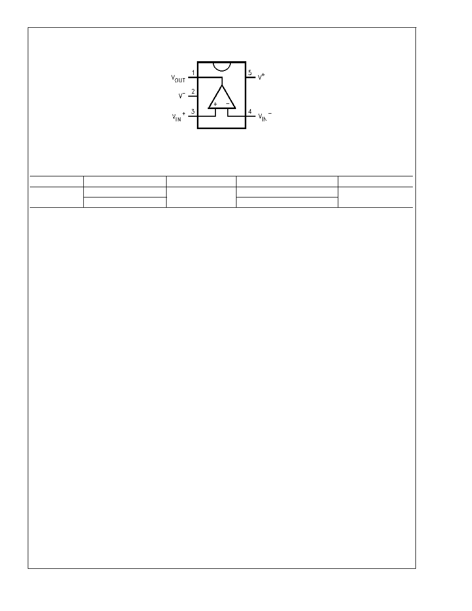
Connection Diagram
5-Pin SOT23
20086223
Top View
Ordering Information
Package
Part Number
Package Marking
Transport Media
NSC Drawing
5-Pin SOT23
LMH6640MF
AH1A
1k Units Tape and Reel
MF05A
LMH6640MFX
3k Units Tape and Reel
LMH6640
www.national.com
5
Document Outline