LMH6678
Low Power 2-Channel Central-Office xDSL Driver
General Description
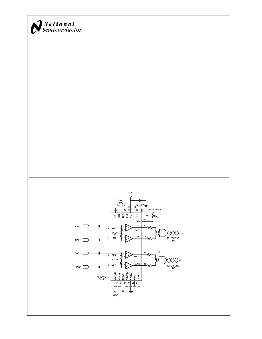
The LMH6678 is a low power 2-channel differential output
driver utilizing dual current feedback op amps with a fixed
gain of A
V
= +5.4.
The LMH6678 utilizes high integration with low power con-
sumption to provide 580 mW at 19.8 dBm line output. The
LMH6678 can also be put into a listen mode to maintain the
termination for receive signals with 100 mW/Ch power dis-
sipation.
The LMH6678 has two separate 2-bit power control inputs
compatible with 3.3V CMOS for each channel that enable
independent control of line status. When the drivers for both
channels are shut off, power consumption drops to only 6
mW.
Thermal Shutdown function protects the IC from a shorted
line fault or system over temperature.
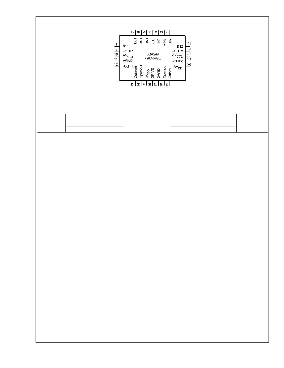
The LMH6678 is available in a 5mm x 4mm 24-lead LLP
package.
Features
AV
CC1
= AV
CC2
= +12V, AV
DD
= DV
DD
= +3.3V, T
A
= 25°C,
2/3 Power Mode, Typical values unless specified.
n
Low power consumption
-- Line power P
LINE
= 100 mW
580 mW/Ch
-- No signal
185 mW/Ch
-- Listen mode
100 mW/Ch
-- Shutdown mode
3 mW/Ch
n
Power Supply
-- Analog (AV
CC1
, AV
CC2
)
+12V
-- Digital (DV
DD
, AV
DD
)
+3.3V
n
Output voltage swing
@
R
L
= 31
-- Single ended
11.5 V
PP
-- Differential
23 V
PP
n
Multi tone power ratio, f = 500 kHz
72 dB
n
Output current
580 mA
n
Thermal shutdown protection
n
5mm x 4mm LLP package
n
Low thermal resistance
36°C/W (
JA
)
n
Small PCB footprint
Application
n
Full rate ADSL, ADSL+, ADSL++ or G. Lite linecard
n
Remote DSLAMs
Block Diagram
20084037
December 2003
LMH6678
Low
Power
2-Channel
Central-Office
xDSL
Driver
© 2003 National Semiconductor Corporation
DS200840
www.national.com
Absolute Maximum Ratings
(Note 1)
If Military/Aerospace specified devices are required,
please contact the National Semiconductor Sales Office/
Distributors for availability and specifications.
ESD Tolerance
Human Body Model
2KV (Note 2)
Machine Model
200V (Note 8)
V
IN
Differential
±
3V
Supply Voltages
AV
CC1
AGND or AV
CC2
AGND
+13.2V
DV
DD
DGND
+3.6V
AV
DD
AGND
+3.6V
DGND - AGND
±
0.2V
AV
CC1
AV
CC2
±
0.2V
AV
DD
DV
DD
±
0.2V
Voltage at Input Pin
Analog Input
AV
CC1
(AV
CC2
) +0.8V,
AGND -0.8V
Digital Control Input
DV
DD
+0.8V,
DGND -0.8V
Soldering Information
Infrared or Convection (20 sec.)
235°C
Storage Temperature Range
-65°C to +150°C
Junction Temperature (Note 4)
+150°C
Operating Ratings
(Note 1)
Supply Voltage
AV
CC1
to AGND
+12V
±
10%
AV
CC2
to AGND
+12V
±
10%
DV
DD
to DGND
+3.3V
±
10%
AV
DD
to AGND
+3.3V
±
10%
Operating Temperature Range
(Note 3), (Note 4)
-40°C to +85°C
Package Thermal Resistance (
JA
)
(Note 4)
36°C/W
Electrical Characteristics
Unless otherwise specified, all limits guaranteed for T
J
= 25°C, AV
CC1
= AV
CC2
=
+12V, DV
DD
= AV
DD
= +3.3V. DGND = AGND = 0V, 2/3 Power Mode. See (Note 9).
Symbol
Parameter
Conditions
Min
(Note 6)
Typ
(Note 5)
Max
(Note 6)
Units
Dynamic Performance
f
CL
-3 dB BW
R
L
= 100
50
MHZ
SR
Slew Rate (Note 7)
V
IN_DIFF
=
±
2.4V, R
L
= 100
700
V/µs
Distortion and Noise Response
HD2
2nd Harmonic Distortion
fc = 1 MHz, V
O
= 2 V
PP
, R
L
= 31
-91
dBc
fc = 200 kHz, V
O
= 2 V
PP
, R
L
= 31
-98
HD3
3
rd
Harmonic Distortion
fc = 1 MHz, V
O
= 2 V
PP
, R
L
= 31
-57
dBc
fc = 200 kHz, V
O
= 2 V
PP
, R
L
= 31
-71
MTPR
Multi-Tone Power Ratio
f = 500 kHz
72
dBc
V
IN
Differential Output Noise
100 kHz to 10 MHz
57
nV/
Input Characteristics
V
IN
Input DC Voltage
Common Mode
6.04
6.1
6.16
V
R
IN
Input Resistance
Differential
I
DIFF
= 10 µA from +IN to -IN
14.4
20
28.4
k
Transfer Characteristics
A
V
Voltage Gain
V
IN_DIFF
= -1 to 1V, No Load
+5.37
+5.40
+5.48
V/V
PSRR
Power Supply Rejection Ratio
-108
dB
Xt
Cross Talk
f = 1 MHz, R
L
= 100
-95
V
O
Output Voltage Swing High
V
IN_DIFF
=
±
2.4V, No Load
11.85
V
V
IN_DIFF
=
±
2.4V, R
L
= 31
11.68
11.75
V
IN_DIFF
=
±
2.4V, I
OUT
= 580 mA
11.64
11.74
Output Voltage Swing Low
V
IN_DIFF
=
±
2.4V, No Load
0.15
V
V
IN_DIFF
=
±
2.4V, R
L
= 31
0.25
0.36
V
IN_DIFF
=
±
2.4V, I
OUT
= 580 mA
0.31
0.39
I
SC
Output Short Circuit Current
Sourcing to Ground
+800
mA
Sinking to Ground
-800
LMH6678
www.national.com
2
Electrical Characteristics
Unless otherwise specified, all limits guaranteed for T
J
= 25°C, AV
CC1
= AV
CC2
=
+12V, DV
DD
= AV
DD
= +3.3V. DGND = AGND = 0V, 2/3 Power Mode. See (Note 9). (Continued)
Symbol
Parameter
Conditions
Min
(Note 6)
Typ
(Note 5)
Max
(Note 6)
Units
I
OUT
Output Current
V
IN_DIFF
=
±
2.4V
Sourcing, R
L
= 20
Sinking, R
L
= 20
±
580
mA
V
OC
Output Common Mode Voltage
5.89
6
6.05
V
V
OS
Output Offset Voltage
-40
0
+40
mV
Power Supply (Note 10), (Note 11)
I
CC
AV
CC
Quiescent Supply Current
B01
B11
B02
B12
Full Power
L
L
L
L
28.6
33
36.9
mA
2/3 Power
H
L
H
L
18.6
22
25.4
1/3 Power
L
H
L
H
9.2
12
14.3
Shutdown
H
H
H
H
0.2
.95
I
DV
DV
DD
Quiescent Supply Current
B01
B11
B02
B12
mA
Full Power
L
L
L
L
11
16
19
2/3 Power
H
L
H
L
7
12
15
1/3 Power
L
H
L
H
3
7
10.3
Shutdown
H
H
H
H
0.05
.14
I
AV
AV
DD
Quiescent Supply Current
All Power Modes
.8
1.1
1.4
mA
Logic Inputs
V
IH
Input High Voltage
2.7
3.3
V
V
IL
Input Low Voltage
0
0.5
V
I
IH
Input High Current
@
V
IH
= 3.3V
-0.5
0.02
+0.5
µA
I
IL
Input Low Current
@
V
IH
= 0V
-0.5
0.02
+0.5
µA
Charge Pump
f
CP
Charge Pump Frequency
Measure at DRIVE at Full Power
2.43
2.75
MHz
V
HIGH
Charge Pump High Average
Voltage
Measure at CstoreH at Full Power
+14.6
V
V
LOW
Charge Pump Low Average
Voltage
Measure at CstoreL at Full Power
-2.7V
V
Note 1: Absolute maximum ratings indicate limits beyond which damage to the device may occur. Operating Ratings indicate conditions for which the device is
intended to be functional, but specific performance is not guaranteed. For guaranteed specifications and the test conditions, see the Electrical Characteristics.
Note 2: Human body model, 1.5k
in series with 100pF.
Note 3: Continuous short circuit operation at elevated ambient temperature can result in exceeding the maximum allowed junction temperature of 150° C.
Note 4: The maximum power dissipation is a function of T
J(MAX)
,
JA
, and T
A
. The maximum allowable power dissipation at any ambient temperature is P
D
=
(T
J(MAX)
- T
A
)/
JA
. All numbers apply for packages soldered directly onto a PC board. Die attach pad is electrically connected to AGND.
Note 5: Typical Values represent the most likely parametric norm.
Note 6: All limits are guaranteed by testing or statistical analysis.
Note 7: Slew rate is the slowest of the rising and falling slew rates.
Note 8: Machine Model, 0
in series with 200 pF.
Note 9: Electrical table values apply only for factory testing conditions at the temperature indicated. Factory testing conditions result in very limited self-heating of
the device such that T
J
= T
A
. No guarantee of parametric performance is indicated in the electrical tables under conditions of internal self heating where T
J
>
T
A
.
Absolute maximum ratings indicate junction temperature limits beyond which the device may be permanently degraded, either mechanically or electrically.
Note 10: Quiescent supply current specification apply for the condition of no input signal. See application section for information on power consumption as a
function of output power, power control bit settings and external resistor R
ADJ
.
Note 11: "L" is V
IL
and "H" is V
IH
.
LMH6678
www.national.com
3
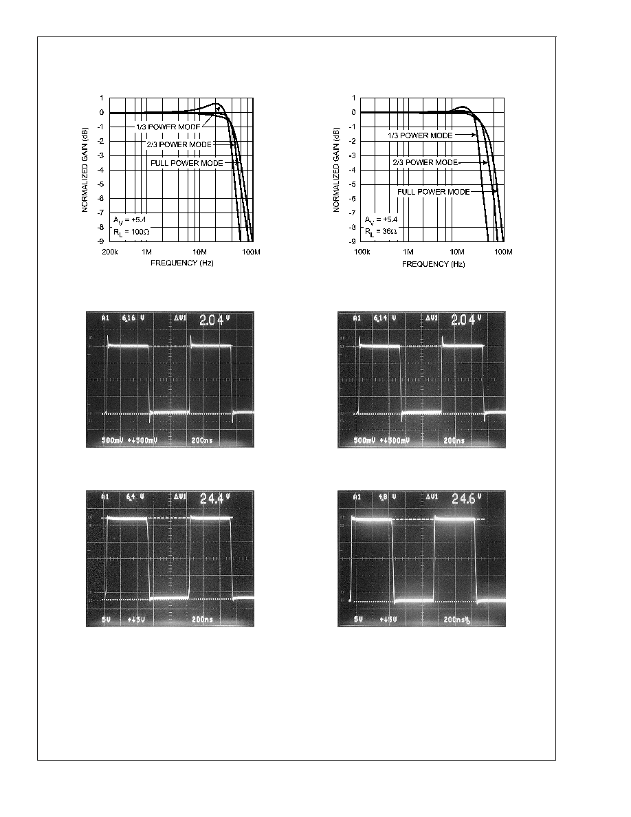
Typical Performance Characteristics
Single-Ended Small Signal Frequency Response
@
R
L
= 100
Single-Ended Small Signal Frequency Response
@
R
L
= 36
20084010
20084011
Medium Signal Pulse Response
@
R
L
= 100
, 1 MHz
Medium Signal Pulse Response
@
R
L
= 36
, 1 MHz
20084005
20084006
Large Signal Pulse Response
@
R
L
= 100
, 1 MHz
Large Signal Pulse Response
@
R
L
= 36
, 1 MHz
20084008
20084007
LMH6678
www.national.com
5