Äîêóìåíòàöèÿ è îïèñàíèÿ www.docs.chipfind.ru
LMH6738
Very Wideband, Low Distortion Triple Op Amp
General Description
The LMH6738 is a very wideband, DC coupled monolithic
operational amplifier designed specifically for ultra high reso-
lution video systems as well as wide dynamic range systems
requiring exceptional signal fidelity. Benefiting from Nation-
al's current feedback architecture, the LMH6738 offers a
gain range of
±
1 to
±
10 while providing stable, operation
without external compensation, even at unity gain. At a gain
of +2 the LMH6738 supports ultra high resolution video
systems with a 400 MHz 2 V
PP
3 dB Bandwidth. With 12-bit
distortion levels through 30 MHz (R
L
= 100
), 2.3 nV/
Hz input referred noise, the LMH6738 is the ideal driver or
buffer for high speed flash A/D and D/A converters. Wide
dynamic range systems such as radar and communication
receivers requiring a wideband amplifier offering exceptional
signal purity will find the LMH6738's low input referred noise
and low harmonic distortion make it an attractive solution.
Features
n
750 MHz -3 dB small signal bandwidth (A
V
= +1)
n
-85 dBc 3rd harmonic distortion (20 MHz)
n
2.3 nV/
Hz input noise voltage
n
3300 V/µs slew rate
n
33 mA supply current (11.3 mA per op amp)
n
90 mA linear output current
n
0.02/0.01 Diff. Gain / Diff. Phase (R
L
= 150
)
Applications
n
RGB video driver
n
High resolution projectors
n
Flash A/D driver
n
D/A transimpedance buffer
n
Wide dynamic range IF amp
n
Radar/communication receivers
n
DDS post-amps
n
Wideband inverting summer
n
Line driver
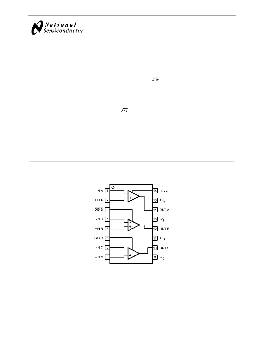
Connection Diagram
16-Pin SSOP
20097510
Top View
VIP10
TM
is a trademark of National Semiconductor Corporation.
July 2004
LMH6738
V
ery
W
ideband,
Low
Distortion
T
riple
Op
Amp
© 2004 National Semiconductor Corporation
DS200975
www.national.com
Absolute Maximum Ratings
(Note 1)
If Military/Aerospace specified devices are required,
please contact the National Semiconductor Sales Office/
Distributors for availability and specifications.
Supply Voltage (V
+
- V
)
13.2V
I
OUT
(Note 3)
Common Mode Input Voltage
±
V
CC
Maximum Junction Temperature
+150°C
Storage Temperature Range
-65°C to +150°C
Soldering Information
Infrared or Convection (20 sec.)
235°C
Wave Soldering (10 sec.)
260°C
ESD Tolerance (Note 4)
Human Body Model
2000V
Machine Model
200V
Storage Temperature Range
-65°C to +150°C
Operating Ratings
(Note 1)
Thermal Resistance
Package
(
JC
)
(
JA
)
16-Pin SSOP
36°C/W
120°C/W
Operating Temperature Range
-40°C
+85°C
Supply Voltage (V
+
- V
)
8V
to
12V
Electrical Characteristics
(Note 2)
A
V
= +2, V
CC
=
±
5V, R
L
= 100
, R
F
= 549
; unless otherwise specified.
Symbol
Parameter
Conditions
Min
Typ
Max
Units
Frequency Domain Performance
UGBW
-3 dB Bandwidth
Unity Gain, V
OUT
= 200 mV
PP
750
MHz
SSBW
-3 dB Bandwidth
V
OUT
= 200 mV
PP
480
MHz
LSBW
V
OUT
= 2 V
PP
400
0.1 dB Bandwidth
V
OUT
= 2 V
PP
150
MHz
GFPL
Peaking
DC to 75 MHz
0
dB
GFR1
Rolloff
DC to 150 MHz, V
OUT
= 2 V
PP
0.1
dB
GFR2
Rolloff
@
300 MHz, V
OUT
= 2 V
PP
1.0
dB
Time Domain Response
TRS
Rise and Fall Time
(10% to 90%)
2V Step
0.9
ns
TRL
5V Step
1.7
SR
Slew Rate
5V Step
3300
V/µs
t
s
Settling Time to 0.1%
2V Step
10
ns
t
e
Enable Time
From Disable = rising edge.
7.3
ns
t
d
Disable Time
From Disable = falling edge.
4.5
ns
Distortion
HD2L
2
nd
Harmonic Distortion
2 V
PP
, 5 MHz
-80
dBc
HD2
2 V
PP
, 20 MHz
-71
HD2H
2 V
PP
, 50 MHz
-55
HD3L
3
rd
Harmonic Distortion
2 V
PP
, 5 MHz
-90
dBc
HD3
2 V
PP
, 20 MHz
-85
HD3H
2 V
PP
, 50 MHz
-65
Equivalent Input Noise
V
N
Non-Inverting Voltage
>
1 MHz
2.3
nV/
I
CN
Inverting Current
>
1 MHz
12
pA/
N
CN
Non-Inverting Current
>
1 MHz
3
pA/
Video Performance
DG
Differential Gain
4.43 MHz, R
L
= 150
.02
%
DP
Differential Phase
4.43 MHz, R
L
= 150
.01
°
Static, DC Performance
VIO
Input Offset Voltage (Note 6)
0.5
±
2.5
±
4.5
mV
IBN
Input Bias Current (Note 6)
Non-Inverting
-15
-20
-7
0
+5
µA
IBI
Input Bias Current (Note 6)
Inverting
-2
±
25
±
35
µA
LMH6738
www.national.com
2
Electrical Characteristics
(Note 2) (Continued)
A
V
= +2, V
CC
=
±
5V, R
L
= 100
, R
F
= 549
; unless otherwise specified.
Symbol
Parameter
Conditions
Min
Typ
Max
Units
PSRR
Power Supply Rejection Ratio
(Note 6)
50
48.5
53
dB
CMRR
Common Mode Rejection Ratio
(Note 6)
46
44
50
dB
XTLK
Crosstalk
Input Referred, f=10MHz, Drive
channels A,C measure channel
B
-80
dB
I
CC
Supply Current (Note 6)
All three amps Enabled, No
Load
32
35
40
mA
Supply Current Disabled V
+
R
L
=
1.9
2.2
mA
Supply Current Disabled V
-
R
L
=
1.1
1.3
mA
Miscellaneous Performance
R
IN
+
Non-Inverting Input Resistance
1000
k
C
IN
+
Non-Inverting Input Capacitance
.8
pF
R
IN
-
Inverting Input Impedance
Output impedance of input
buffer.
30
R
O
Output Impedance
DC
0.05
V
O
Output Voltage Range (Note 6)
R
L
= 100
±
3.25
±
3.1
±
3.5
V
R
L
=
±
3.65
±
3.5
±
3.8
CMIR
Common Mode Input Range
(Note 6)
CMRR
>
40 dB
±
1.9
±
1.7
±
2.0
V
I
O
Linear Output Current
(Notes 3, 6)
V
IN
= 0V, V
OUT
<
±
30 mV
80
60
90
mA
I
SC
Short Circuit Current (Note 5)
V
IN
= 2V Output Shorted to
Ground
160
mA
I
IH
Disable Pin Bias Current High
Disable Pin = V
+
10
µA
I
IL
Disable Pin Bias Current Low
Disable Pin = 0V
-350
µA
V
DMAX
Voltage for Disable
Disable Pin
V
DMAX
0.8
V
V
DMIM
Voltage for Enable
Disable Pin
V
DMIN
2.0
V
Note 1: Absolute Maximum Ratings indicate limits beyond which damage to the device may occur. Operating Ratings indicate conditions for which the device is
intended to be functional, but specific performance is not guaranteed. For guaranteed specifications, see the Electrical Characteristics tables.
Note 2: Electrical Table values apply only for factory testing conditions at the temperature indicated. Factory testing conditions result in very limited self-heating of
the device such that T
J
= T
A
. No guarantee of parametric performance is indicated in the electrical tables under conditions of internal self heating where T
J
>
T
A
.
See Applications Section for information on temperature de-rating of this device." Min/Max ratings are based on product characterization and simulation. Individual
parameters are tested as noted.
Note 3: The maximum output current (I
OUT
) is determined by device power dissipation limitations. See the Power Dissipation section of the Application Section for
more details.
Note 4: Human body model: 1.5 k
in series with 100 pF. Machine model: 0 in series with 200 pF.
Note 5: Short circuit current should be limited in duration to no more than 10 seconds. See the Power Dissipation section of the Application Section for more details.
Note 6: Parameter 100% production tested at 25° C.
Ordering Information
Package
Part Number
Package Marking
Transport Media
NSC Drawing
16-pin SSOP
LMH6738MQ
LH6738MQ
95 Units/Rail
MQA16
LMH6738MQX
2.5k Units Tape and Reel
LMH6738
www.national.com
3
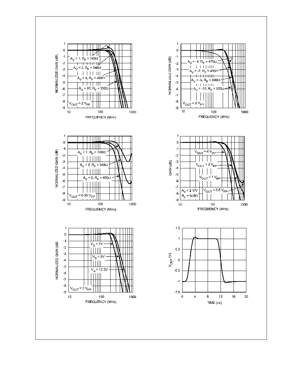
Typical Performance Characteristics
A
V
= +2, V
CC
=
±
5V, R
L
= 100
, R
F
= 549
; unless other-
wise specified).
Large Signal Frequency Response
Large Signal Frequency Response
20097520
20097528
Small Signal Frequency Response
Frequency Response vs. V
OUT
20097513
20097501
Frequency Response vs. Supply Voltage
Pulse Response
20097516
20097522
LMH6738
www.national.com
4
Typical Performance Characteristics
A
V
= +2, V
CC
=
±
5V, R
L
= 100
, R
F
= 549
; unless otherwise
specified). (Continued)
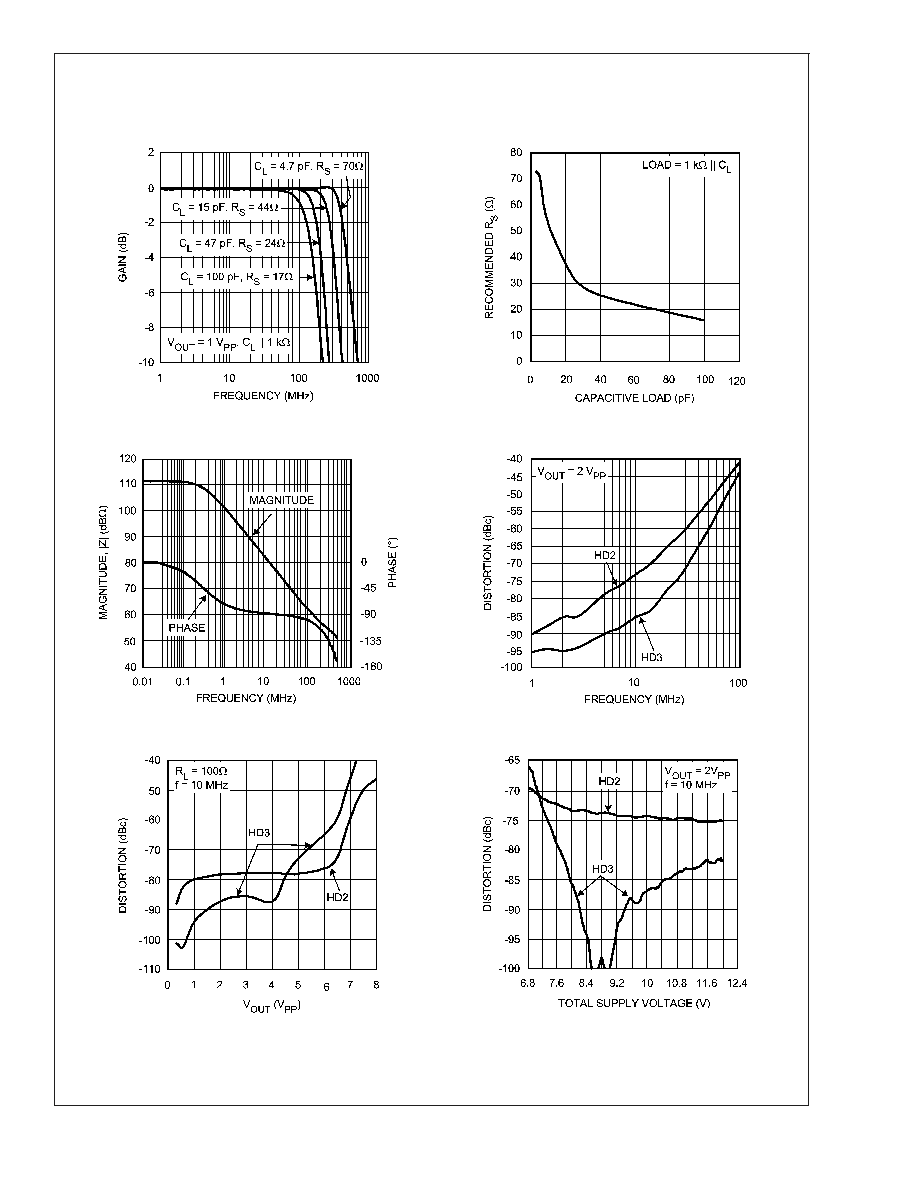
Frequency Response vs. Capacitive Load
Series Output Resistance vs. Capacitive Load
20097514
20097519
Open Loop Gain and Phase
Distortion vs. Frequency
20097526
20097525
Distortion vs. Output Voltage
Distortion vs. Supply Voltage
20097517
20097518
LMH6738
www.national.com
5
Document Outline