LMP7701
Precision, CMOS Input, RRIO, Wide Supply Range
Amplifier
General Description
The LMP7701 is a single, low offset voltage, rail-to-rail input
and output precision amplifier with a CMOS input stage and
a wide supply voltage range. The LMP7701 is part of the
LMP
TM
precision amplifier family and is ideal for sensor
interface and other instrumentation applications.
The guaranteed low offset voltage of less than
±
200 µV
along with the guaranteed low input bias current of less than
±
10 pA make the LMP7701 ideal for precision applications.
The LMP7701 is built utilizing VIP50 technology, which al-
lows the combination of a CMOS input stage and a 12V
common mode and supply voltage range. This makes the
LMP7701 a great choice in many applications where con-
ventional CMOS parts cannot operate under the desired
voltage conditions.
The LMP7701 has a rail-to-rail input stage that significantly
reduces the CMRR glitch commonly associated with rail-to-
rail input amplifiers. This is achieved by trimming both sides
of the complimentary input stage, thereby reducing the dif-
ference between the NMOS and PMOS offsets. The output
of the LMP7701 swings within 40 mV of either rail to maxi-
mize the signal dynamic range in applications requiring low
supply voltage.
The LMP7701 is offered in space saving SOT23-5. This
small package is an ideal solution for area constrained PC
boards and portable electronics.
Features
Unless otherwise noted, typical values at V
S
= 5V
n
Input offset voltage
±
200 µV (max)
n
Input bias current
300 fA
n
Input voltage noise
12 nV/
n
CMRR
100 dB
n
Open loop gain
130 dB
n
Temperature range
≠40∞C to 125∞C
n
Unity gain bandwidth
2.5 MHz
n
Supply current
715 µA
n
Supply Voltage Range
2.7V to 12V
n
Rail-to-rail input and output
Applications
n
High impedance sensor interface
n
Battery powered instrumentation
n
High gain amplifiers
n
DAC buffer
n
Instrumentation amplifier
n
Active filters
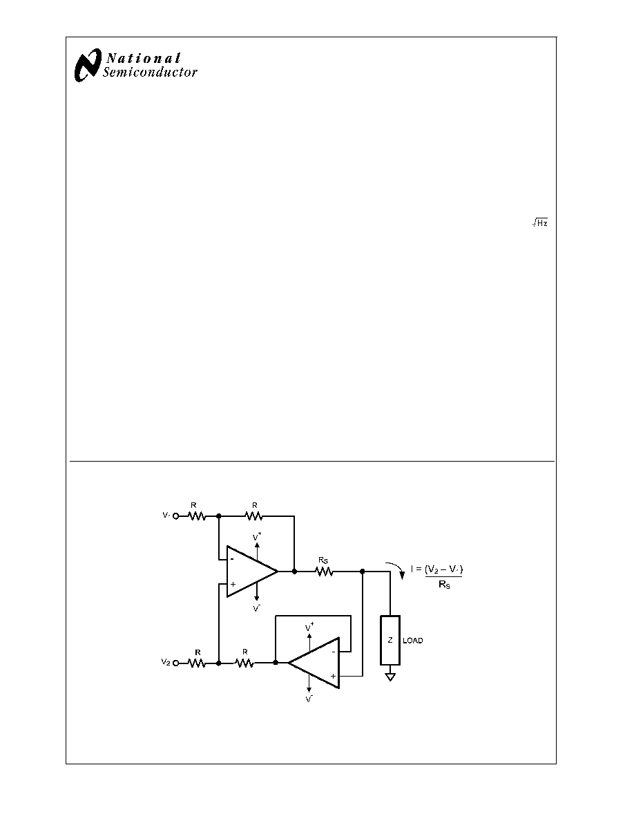
Typical Application
20127305
Precision Current Source
LMP
TM
is a trademark of National Semiconductor Corporation.
PRELIMINARY
September 2005
LMP7701
Precision,
CMOS
Input,
RRIO,
W
ide
Supply
Range
Amplifier
© 2005 National Semiconductor Corporation
DS201273
www.national.com
Absolute Maximum Ratings
(Note 1)
If Military/Aerospace specified devices are required,
please contact the National Semiconductor Sales Office/
Distributors for availability and specifications.
ESD Tolerance (Note 2)
Human Body Model
2 kV
Machine Model
200V
V
IN
Differential
±
300 mV
Supply Voltage (V
S
= V
+
≠ V
-
)
13.2V
Voltage at Input/Output Pins
V
+
+ 0.3V, V
-
- 0.3V
Input Current
10 mA
Storage Temperature Range
-65∞C to +150∞C
Junction Temperature (Note 3)
+150∞C
Soldering Information
Infrared or Convection (20 sec)
235∞C
Wave Soldering Lead Temp. (10
sec)
260∞C
Operating Ratings
(Note 1)
Temperature Range (Note 3)
-40∞C to +125∞C
Supply Voltage (V
S
= V
+
≠ V
-
)
2.7V to 12V
Package Thermal Resistance (
JA
(Note 3))
5-Pin SOT23
234∞C/W
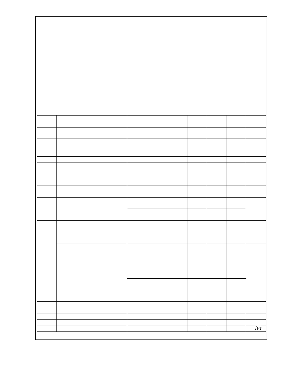
3V Electrical Characteristics
(Note 4)
Unless otherwise specified, all limits are guaranteed for T
A
= 25∞C, V
+
= 3V, V
-
= 0V, V
CM
= V
+
/2, and R
L
>
10 k
to V
+
/2.
Boldface limits apply at the temperature extremes.
Symbol
Parameter
Conditions
Min
(Note 6)
Typ
(Note 5)
Max
(Note 6)
Units
V
OS
Input Offset Voltage
±
37
±
200
±
500
µV
TCV
OS
Input Offset Voltage Drift
(Note 7)
±
1
±
5
µV/∞C
I
B
Input Bias Current
(Notes 7, 8)
0.3
10
300
pA
I
OS
Input Offset Current
40
fA
CMRR
Common Mode Rejection Ratio
0V
V
CM
3V
86
80
98
dB
PSRR
Power Supply Rejection Ratio
2.7V
V
+
12V, Vo = V
+
/2
86
82
98
dB
CMVR
Input Common-Mode Voltage Range
CMRR
80 dB
CMRR
77 dB
≠0.2
≠0.2
3.2
3.2
V
A
VOL
Large Signal Voltage Gain
R
L
= 2 k
V
O
= 0.3V to 2.7V
100
96
114
dB
R
L
= 10 k
V
O
= 0.2V to 2.8V
100
96
124
V
O
Output Swing High
R
L
= 2 k
to V
+
/2
2.92
2.88
2.96
V
R
L
= 10 k
to V
+
/2
2.96
2.94
2.97
Output Swing Low
R
L
= 2 k
to V
+
/2
0.04
0.06
0.08
V
R
L
= 10 k
to V
+
/2
0.02
0.04
0.05
I
O
Output Short Circuit Current
(Notes 3, 9)
Sourcing V
O
= 0V
V
IN
= 100 mV
25
15
42
mA
Sinking V
O
= 3V
V
IN
= -100 mV
25
20
42
I
S
Supply Current
0.670
1.0
1.2
mA
SR
Slew Rate (Note 10)
A
V
= +1, V
O
= 2 V
PP
10% to 90%
0.9
V/µs
GBW
Gain Bandwidth Product
2.5
MHz
THD+N
Total Harmonic Distortion + Noise
f = 1 kHz, Av = 1, R
L
= 1 k
0.02
%
e
n
Input-Referred Voltage Noise
f = 1 kHz
12
nV/
LMP7701
www.national.com
2
3V Electrical Characteristics
(Note 4)
(Continued)
Unless otherwise specified, all limits are guaranteed for T
A
= 25∞C, V
+
= 3V, V
-
= 0V, V
CM
= V
+
/2, and R
L
>
10 k
to V
+
/2.
Boldface limits apply at the temperature extremes.
Symbol
Parameter
Conditions
Min
(Note 6)
Typ
(Note 5)
Max
(Note 6)
Units
i
n
Input-Referred Current Noise
f = 100 kHz
1
fA/
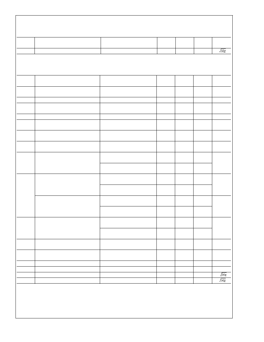
5V Electrical Characteristics
(Note 4)
Unless otherwise specified, all limits are guaranteed for T = 25∞C, V
+
= 5V, V
-
= 0V, V
CM
= V
+
/2, and R
L
>
10 k
to V
+
/2.
Boldface limits apply at the temperature extremes.
Symbol
Parameter
Conditions
Min
(Note 6)
Typ
(Note 5)
Max
(Note 6)
Units
V
OS
Input Offset Voltage
±
37
±
200
±
500
µV
TCV
OS
Input Offset Voltage Drift
(Note 7)
±
1
±
5
µV/∞C
I
B
Input Bias Current
(Notes 7, 8)
0.3
10
300
pA
I
OS
Input Offset Current
40
fA
CMRR
Common Mode Rejection Ratio
0V
V
CM
5V
88
83
100
dB
PSRR
Power Supply Rejection Ratio
2.7V
V
+
12V, Vo = V
+
/2
86
82
98
dB
CMVR
Input Common-Mode Voltage Range
CMRR
80 dB
CMRR
78 dB
≠0.2
≠0.2
5.2
5.2
V
A
VOL
Large Signal Voltage Gain
R
L
= 2 k
V
O
= 0.3V to 4.7V
100
96
119
dB
R
L
= 10 k
V
O
= 0.2V to 4.8V
100
96
130
V
O
Output Swing High
R
L
= 2 k
to V
+
/2
4.89
4.87
4.94
V
R
L
= 10 k
to V
+
/2
4.95
4.93
4.96
Output Swing Low
R
L
= 2 k
to V
+
/2
0.05
0.08
0.09
V
R
L
= 10 k
to V
+
/2
0.03
0.04
0.05
I
O
Output Short Circuit Current
(Notes 3, 9)
Sourcing V
O
= 0V
V
IN
= 100 mV
40
28
66
mA
Sinking V
O
= 5V
V
IN
= -100 mV
40
28
76
I
S
Supply Current
0.715
1.0
1.2
mA
SR
Slew Rate (Note 10)
A
V
= +1, V
O
= 4 V
PP
10% to 90%
1.0
V/µs
GBW
Gain Bandwidth Product
2.5
MHz
THD+N
Total Harmonic Distortion + Noise
f = 1 kHz, Av = 1, R
L
= 1 k
0.02
%
e
n
Input-Referred Voltage Noise
f = 1 kHz
12
nV/
i
n
Input-Referred Current Noise
f = 100 kHz
1
fA/
LMP7701
www.national.com
3
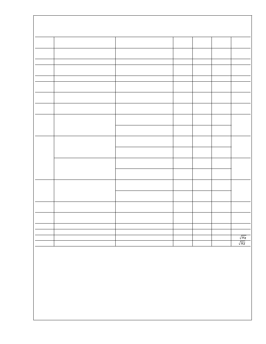
±
5V Electrical Characteristics
(Note 4)
Unless otherwise specified, all limits are guaranteed for T
A
= 25∞C, V
+
= 5V, V
-
= ≠5 V, V
CM
=0, and R
L
>
10 k
to V
CM
.
Boldface limits apply at the temperature extremes.
Symbol
Parameter
Conditions
Min
(Note 6)
Typ
(Note 5)
Max
(Note 6)
Units
V
OS
Input Offset Voltage
±
37
±
200
±
500
µV
TCV
OS
Input Offset Voltage Drift
(Note 7)
±
1
±
5
µV/∞C
I
B
Input Bias Current
(Notes 7, 8)
0.3
10
300
pA
I
OS
Input Offset Current
40
fA
CMRR
Common Mode Rejection Ratio
≠5V
V
CM
5V
92
88
110
dB
PSRR
Power Supply Rejection Ratio
2.7V
V
+
12V, Vo = V
CM
86
82
98
dB
CMVR
Input Common-Mode Voltage
Range
CMRR
80 dB
CMRR
78dB
≠5.2
≠5.2
5.2
5.2
V
A
VOL
Large Signal Voltage Gain
R
L
= 2 k
V
O
= ≠4.7V to 4.7V
100
98
121
dB
R
L
= 10 k
V
O
= ≠4.8V to 4.8V
100
98
134
V
O
Output Swing High
R
L
= 2 k
to V
CM
4.85
4.83
4.91
V
R
L
= 10 k
to V
CM
4.92
4.90
4.96
Output Swing Low
R
L
= 2 k
to V
CM
-4.91
-4.87
-4.85
V
R
L
= 10 k
to V
CM
-4.96
-4.95
-4.94
I
O
Output Short Circuit Current
(Notes 3, 9)
Sourcing V
O
= ≠5V
V
IN
= 100 mV
50
35
86
mA
Sinking V
O
= 5V
V
IN
= -100 mV
50
35
84
I
S
Supply Current
0.790
1.1
1.3
mA
SR
Slew Rate (Note 10)
A
V
= +1, V
O
= 9 V
PP
10% to 90%
1.1
V/µs
GBW
Gain Bandwidth Product
2.5
MHz
THD+N
Total Harmonic Distortion + Noise
f = 1 kHz, Av = 1, R
L
= 1 k
0.02
%
e
n
Input-Referred Voltage Noise
f = 1 kHz
12
nV/
i
n
Input-Referred Current Noise
f = 100 kHz
1
fA/
Note 1: Absolute Maximum Ratings indicate limits beyond which damage to the device may occur. Operating Ratings indicate conditions for which the device is
intended to be functional, but specific performance is not guaranteed. For guaranteed specifications and the test conditions, see the Electrical Characteristics Tables.
Note 2: Human Body Model: 1.5 k
in series with 100 pF. Machine Model: 0 in series with 200 pF.
Note 3: The maximum power dissipation is a function of T
J(MAX)
,
JA
, and T
A
. The maximum allowable power dissipation at any ambient temperature is
P
D
= (T
J(MAX)
- T
A
)/
JA
. All numbers apply for packages soldered directly onto a PC board.
Note 4: Electrical table values apply only for factory testing conditions at the temperature indicated. Factory testing conditions result in very limited self-heating of
the device.
Note 5: Typical values represent the parametric norm at the time of characterization.
Note 6: Limits are 100% production tested at 25∞C. Limits over the operating temperature range are guaranteed through correlations using the Statistical Quality
Control (SQC) method.
Note 7: Guaranteed by design.
Note 8: Positive current corresponds to current flowing into the device.
Note 9: The short circuit test is a momentary test.
Note 10: The number specified is the slower of positive and negative slew rates.
LMP7701
www.national.com
4
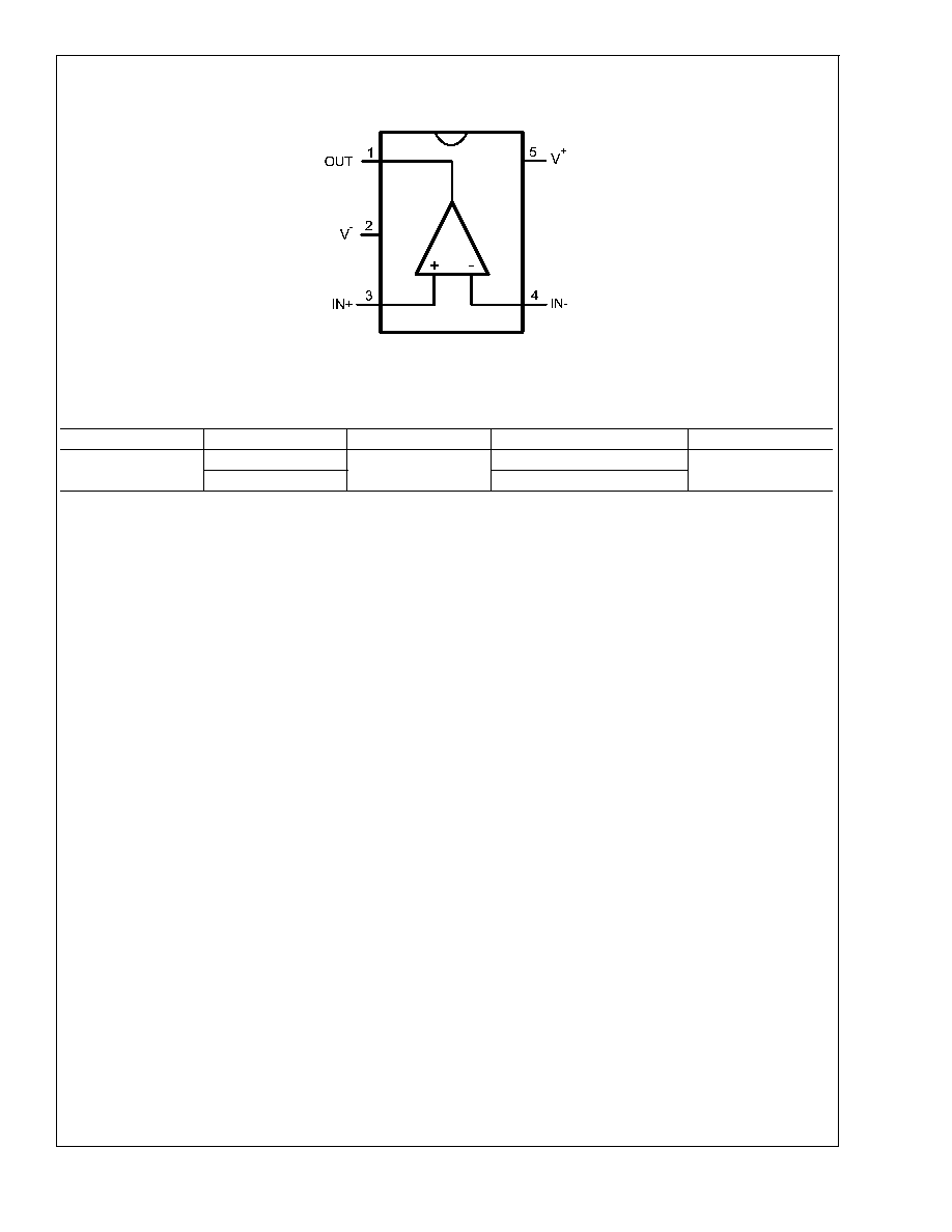
Connection Diagram
5-Pin SOT23
20127302
Top View
Ordering Information
Package
Part Number
Package Marking
Transport Media
NSC Drawing
5-Pin SOT-23
LMP7701MF
AC2A
1k Units Tape and Reel
MF05A
LMP7701MFX
3k Units Tape and Reel
LMP7701
www.national.com
5