 | –≠–ª–µ–∫—Ç—Ä–æ–Ω–Ω—ã–π –∫–æ–º–ø–æ–Ω–µ–Ω—Ç: LMS485EIM | –°–∫–∞—á–∞—Ç—å:  PDF PDF  ZIP ZIP |
LMS485E
Low Power RS-485 / RS-422 Differential Bus Transceiver
General Description
The LMS485E is a low power differential bus/line transceiver
designed for high speed bidirectional data communication on
multipoint bus transmission lines. It is designed for balanced
transmission lines. It meets ANSI Standards TIA/EIA
RS422-B, TIA/EIA RS485-A and ITU recommendation and
V.11 and X.27. The driver outputs and receiver inputs have
±
15kV ESD protection. The LMS485E combines a TRI-
STATE
TM
differential line driver and differential input receiver,
both of which operate from a single 5.0V power supply. The
driver and receiver have an active high and active low,
respectively, that can be externally connected to function as
a direction control. The driver outputs and receiver inputs are
internally connected to form a differential input/output (I/O)
bus port that is designed to offer minimum loading to bus
whenever the driver is disabled or when V
CC
= 0V. These
ports feature wide positive and negative common mode
voltage ranges, making the device suitable for multipoint
applications in noisy environments. The LMS485E is avail-
able in 8-Pin SOIC and 8-pin DIP packages. It is a drop-in
replacement to Maxim's MAX485E.
Features
n
Meet ANSI standard RS-485 and RS-422
n
Data rate 2.5 Mbps
n
Single supply voltage operation, 5V
n
Wide input and output voltage range
n
Thermal shutdown protection
n
Short circuit protection
n
Low quiescent current 800µA (max)
n
Allows up to 32 transceivers on the bus
n
Open circuit fail-safe for receiver
n
Extended operating temperature range -40∞C to 85∞C
n
Drop-in replacement to MAX485E
n
Available in 8-pin SOIC and 8-pin DIP packages
Applications
n
Low power RS-485 systems
n
Network hubs, bridges, and routers
n
Point of sales equipment (ATM, barcode scanners,...)
n
Local area networks (LAN)
n
Integrated service digital network (ISDN)
n
Industrial programmable logic controllers
n
High speed parallel and serial applications
n
Multipoint applications with noisy environment
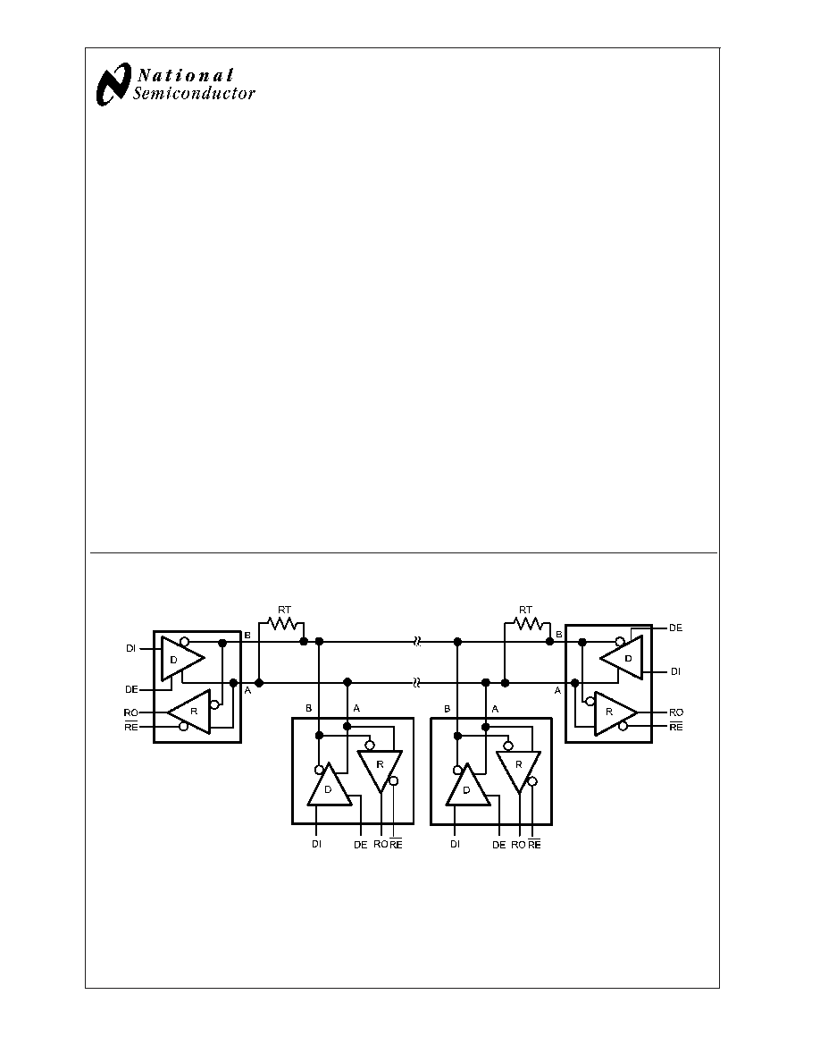
Typical Application
20086601
A typical multipoint application is shown in the above figure. Terminating resistor, RT are typically required but only located at the two ends of the cable.
Pull-up and pull-down resistors maybe required at the end of the bus to provide fail-safe biasing. The biasing resistors provide a bias to the cable when all
drivers are in TRI-STATE, See National Application Note, AN-847 for further information.
November 2003
LMS485E
Low
Power
RS-485
/
RS-422
Differential
Bus
T
ransceiver
© 2003 National Semiconductor Corporation
DS200866
www.national.com
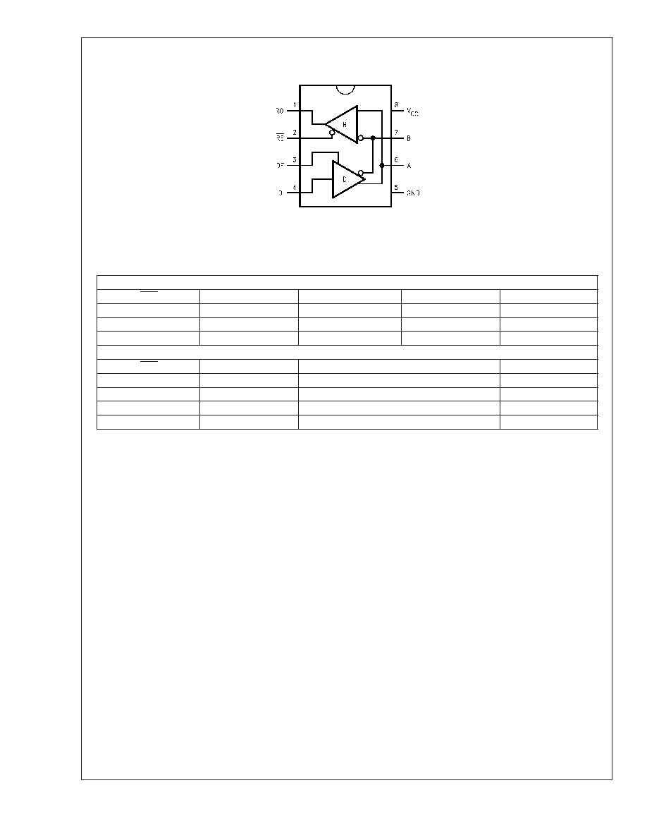
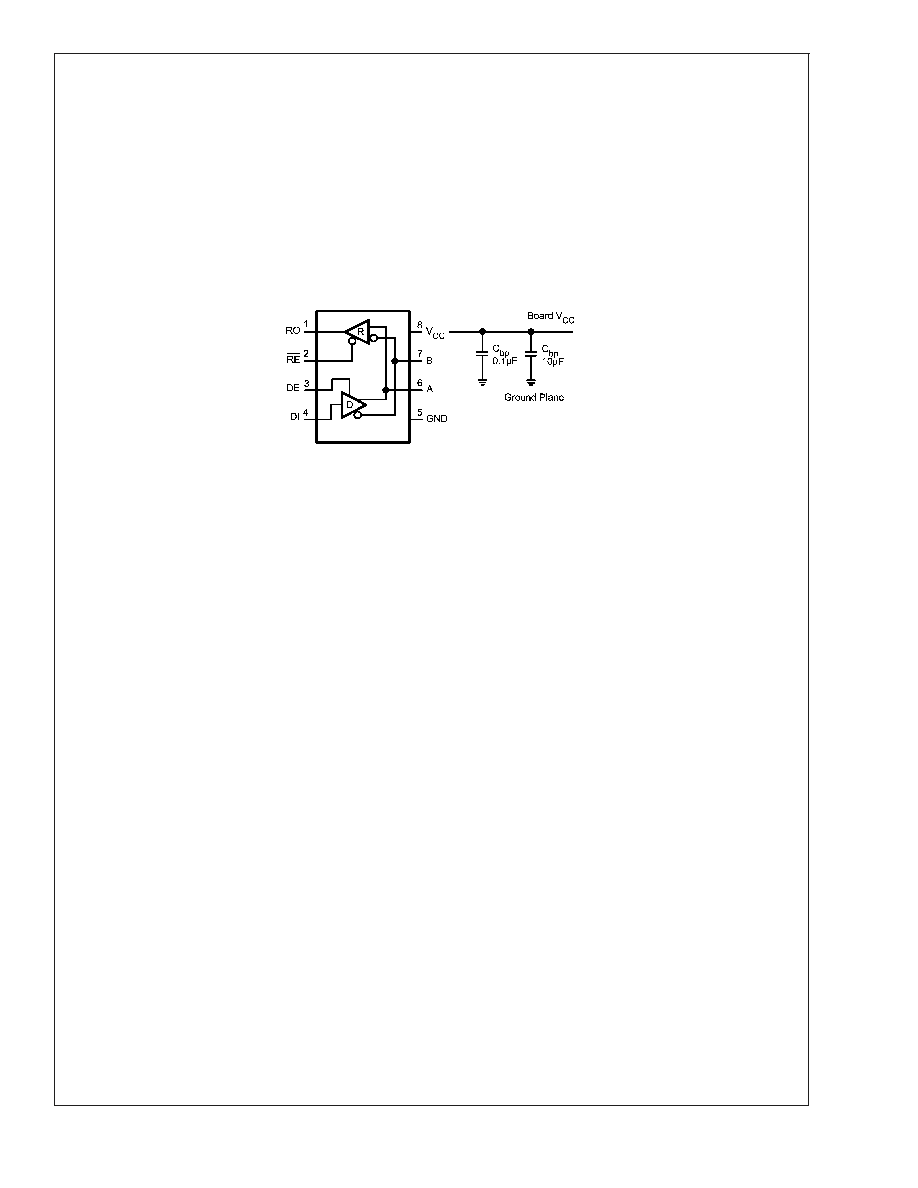
Connection Diagram
8-Pin SOIC / DIP
20086602
Top View
Truth Table
DRIVER SECTION
RE
*
DE
DI
A
B
X
H
H
H
L
X
H
L
L
H
X
L
X
Z
Z
RECEIVER SECTION
RE
*
DE
A-B
RO
L
L
+0.2V
H
L
L
-0.2V
L
H
X
X
Z
L
L
OPEN
*
H
Note: * = Non Terminated, Open Input only
X = Irrelevant
Z = TRI-STATE
H = High level
L = Low level
LMS485E
www.national.com
2
Pin Descriptions
Pin # I/O
Name
Function
1
O
RO
Receiver Output: If A
>
B by 200 mV, RO will be high; If A
<
B by 200 mV, RO will be low. RO
will be high also if the inputs (A and B) are open (non-terminated).
2
I
RE
*
Receiver Output Enable: RO is enabled when RE
*
is low; RO is in TRI-STATEwhen RE
*
is high
3
I
DE
Driver Output Enable: The driver outputs (A and B) are enabled when DE is high; they are in
TRI-STATETRI-STATE
Æ
when DE is low. Pins A and B also function as the receiver input pins
(see below)
4
I
DI
Driver Input: A low on DI forces A low and B high while a high on DI forces A high and B low
when the driver is enabled
5
NA
GND
Ground
6
I/O
A
Non-inverting Driver Output and Receiver Input pin. Driver output levels conform to RS-485
signaling levels
7
I/O
B
Inverting Driver Output and Receiver Input pin. Driver Output levels conform to RS-485 signaling
levels
8
NA
V
CC
Power Supply: 4.75V
V
CC
5.25V
Ordering Information
Package
Part Number
Package Marking
Transport Media
NSC Drawing
8-Pin SOIC
LMS485ECM
LMS485ECM
95 Units/Rail
M08A
LMS485ECMX
2.5k Units Tape and Reel
LMS485EIM
LMS485EIM
95 Units/Rail
LMS485EIMX
2.5k Units Tape and Reel
8-Pin DIP
LMS485ECNA
LMS485ECNA
40 Units/Rail
N08E
LMS485EINA
LMS485EINA
40 Units/Rail
LMS485E
www.national.com
3
Absolute Maximum Ratings
(Note 1)
If Military/Aerospace specified devices are required,
please contact the National Semiconductor Sales Office/
Distributors for availability and specifications.
Supply Voltage, V
CC
(Note 2)
6V
Input Voltage, V
IN
(DI, DE, or RE)
-0.3V to V
CC
+ 0.3V
Voltage Range at Bus Terminals (AB)
-7V to 12V
Receiver Output
-0.3V to V
CC
+ 0.3V
Package Thermal Impedance,
JA
SOIC
125∞ C/W
DIP
92∞ C/W
Junction Temperature (Note 3)
150∞C
Operating Free-Air Temperature
Range, T
A
Commercial
0∞C to 70∞C
Industrial
-40∞C to 85∞C
Storage Temperature Range
-65∞C to 150∞C
Soldering Information
Infrared or Convection (20 sec.)
235∞C
Lead Temperature Range
+260∞C
ESD Rating (Human Body Model)(Note 4)
Bus Pins
15kV
Other Pins
2kV
ESD Rating (Machine Model)
All Pins
200V
Operating Ratings
Min Nom Max
Supply Voltage, V
CC
4.75
5.0
5.25
V
Voltage at any Bus Terminal
(Separately or Common Mode)
-7
12
V
High-Level Input Voltage, V
IH
(Note 5)
2
V
Low-Level Input Voltage, V
IL
(Note 5)
0.8
V
Differential Input Voltage, V
ID
(Note 6)
±
12
V
Electrical Characteristics
Over recommended ranges of supply voltage and operating free-air temperature (unless otherwise noted)
Symbol
Parameter
Conditions
Min
Typ
Max
Units
Driver Section
|V
OD1
|
Differential Output Voltage
R =
(Figure 1)
5.25
V
|V
OD2
|
Differential Output Voltage
R = 50
(Figure 1) , RS-422
2.0
V
R = 27
(Figure 1) , RS-485
1.5
5.0
V
OD
Change in Magnitude of
Driver Differential Output
Voltage for Complementary
Output States
R = 27
or 50 (Figure 1) , (Note 7)
0.2
V
V
OC
Common Mode Output
Voltage
R = 27
or 50 (Figure 1)
3.0
V
V
OC
Change in Magnitude of
Driver Common-Mode Output
Voltage for Complementary
Output States
R = 27
or 50 (Figure 1), (Note 7)
0.2
V
V
IH
CMOS Input Logic Threshold
High
DE, DI, RE
2.0
V
V
IL
CMOS Input Logic Threshold
Low
DE, DI, RE
0.8
V
I
IN1
Logic Input Current
DE, DI, RE
±
2
µA
Receiver Section
I
IN2
Input Current (A, B)
DE = 0V, V
CC
= 0V or 5.25V
V
IN
= 12V
0.25
mA
V
IN
= - 7V
-0.2
V
TH
Differential Input Threshold
Voltage
-7V
V
CM
+ 12V
-0.2
+0.2
V
V
TH
Input Hysteresis
(V
TH+-
V
TH-
)
V
CM
= 0
95
mV
V
OH
CMOS High-level Output
Voltage
I
OH
= 4 mA, V
ID
= -200 mV
3.5
V
LMS485E
www.national.com
4
Electrical Characteristics
(Continued)
Over recommended ranges of supply voltage and operating free-air temperature (unless otherwise noted)
Symbol
Parameter
Conditions
Min
Typ
Max
Units
V
OL
CMOS Low-level Output
Voltage
I
OL
= -4 mA, V
ID
= 200 mV
0.4
V
I
OZR
Tristate Output Leakage
Current
0.4V
V
O
+ 2.4V
±
1
µA
R
IN
Input Resistance
- 7V
V
CM
+12V
12
k
Power Supply Current
I
CC
Supply Current
DE = V
CC,
RE = GND or V
CC
400
800
µA
DE = 0V, RE = GND or V
CC
360
560
I
OSD1
Driver Short-circuit Output
Current
V
O
= high, -7V
V
CM
+12V
250
mA
I
OSD2
Driver Short-circuit Output
Current
V
O
= low, - 7V
V
CM
+12V
250
mA
I
OSR
Receiver Short-circuit Output
Current
0 V
V
O
V
CC
95
mA
Switching Characteristics
Driver
T
PLH
,
T
PHL
Propagation Delay Input to
Output
R
L
= 54
, C
L
= 100 pF
10
40
80
ns
T
SKEW
Driver Output Skew
R
L
= 54
, C
L
= 100 pF
5
10
ns
T
R
,
T
F
Driver Rise and Fall Time
R
L
= 54
, C
L
= 100 pF
3
10
40
ns
T
ZH
,
T
ZL
Driver Enable to Ouput Valid
Time
C
L
= 100 pF
25
70
ns
T
HZ
,
T
LZ
Driver Output Disable Time
C
L
= 15 pF
35
70
ns
Receiver
T
PLH
,
T
PHL
Propagation Delay Input to
Output
R
L
= 54
, C
L
= 100 pF
20
90
200
ns
T
SKEW
Receiver Output Skew
R
L
= 54
, C
L
= 100 pF
5
ns
T
ZH
,
T
ZL
Receiver Enable Time
C
L
= 15 pF
20
50
ns
T
HZ
,
T
LZ
Receiver Disable Time
C
L
= 15 pF
20
50
ns
F
MAX
Maximum Data Rate
2.5
Mbps
Note 1: Absolute Maximum Ratings indicate limits beyond which damage to the device may occur. Operating Ratings indicate conditions for which the device is
intended to be functional, but specific performance is not guaranteed. For guaranteed specifications and the test conditions, see the Electrical Characteristics.
Note 2: All voltage values, except differential I/O bus voltage, are with respect to the network ground terminal.
Note 3: The maximum power dissipation is a function of T
J(MAX)
,
JA
, and T
A
. The maximum allowable power dissipation at any ambient temperature, T
A
, is
P
D
= (T
J(MAX)
- T
A
)/
JA
. All numbers apply for packages soldered directly into a PC board.
Note 4: ESD rating based upon human body model, 100 pF discharged through 1.5 k
.
Note 5: Voltage limits apply to DI, DE, RE pins.
Note 6: Differential input/output bus voltage is measured at the non-inverting terminal A with respect to the inverting terminal B.
Note 7: |
V
OD
| and |
V
OC
| are changes in magnitude of V
OD
and V
OC
, respectively when the input changes from high to low levels.
Note 8: Peak current
LMS485E
www.national.com
5
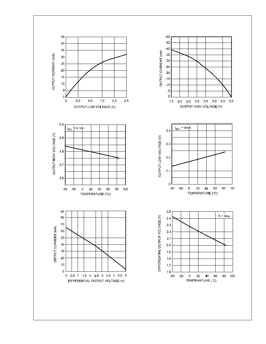
Typical Performance Characteristics
Output Current vs. Receiver Output Low Voltage
Output Current vs. Receiver Output High Voltage
20086613
20086614
Receiver Output High Voltage vs. Temperature
Receiver Output Low-Voltage vs. Temperature
20086615
20086616
Driver Output Current vs. Differential Output Voltage
Driver Differential Output Voltage vs. Temperature
20086617
20086618
LMS485E
www.national.com
6
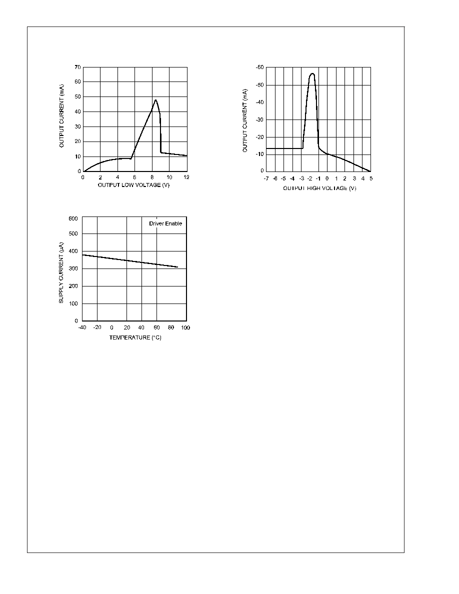
Typical Performance Characteristics
(Continued)
Output Current vs. Driver Output Low Voltage
Output Current vs. Driver Output High Voltage
20086619
20086620
Supply Current vs. Temperature
20086621
LMS485E
www.national.com
7
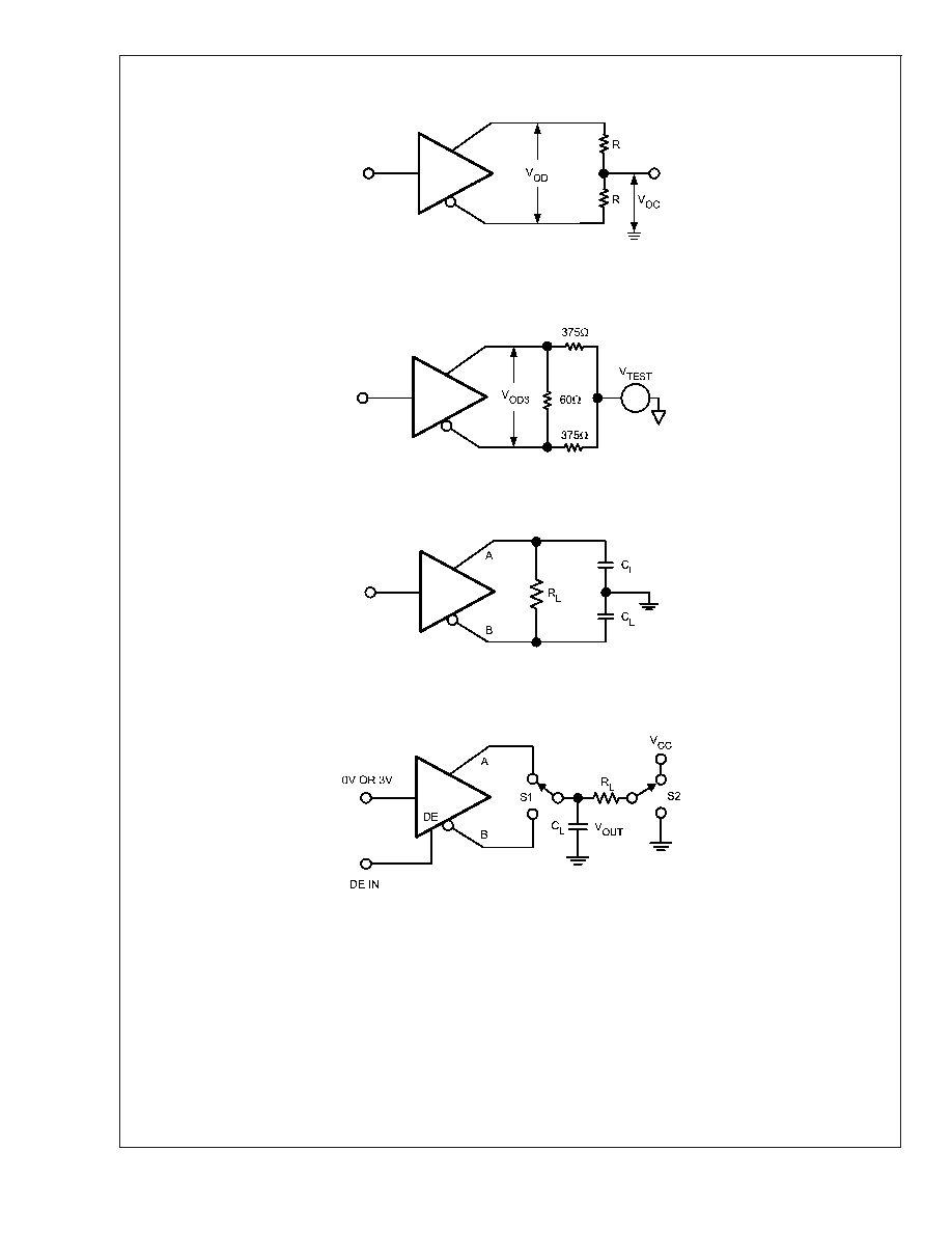
Parameter Measuring Information
20086603
FIGURE 1. Test Circuit for V
OD
and V
OC
20086604
FIGURE 2. Test Circuit for V
OD3
20086605
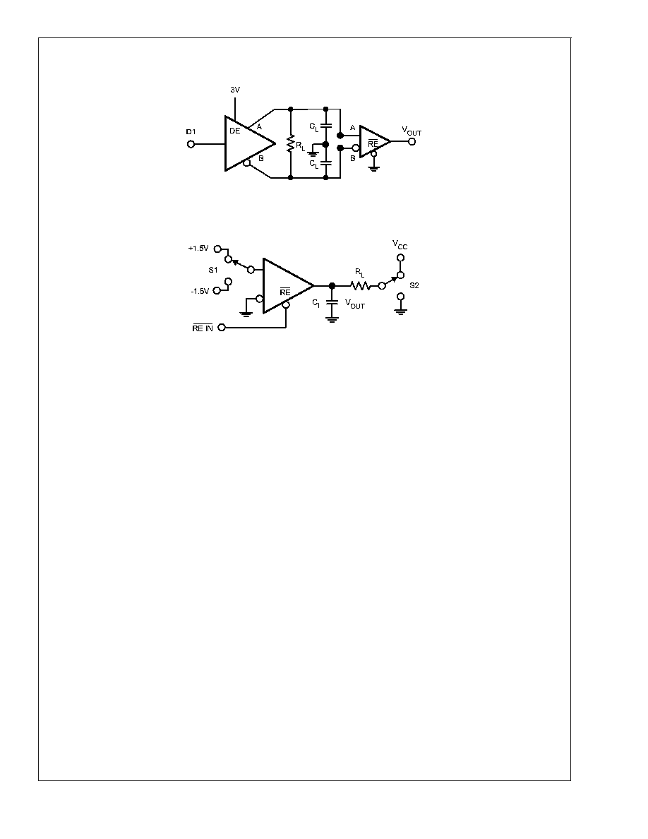
FIGURE 3. Test Circuit for Driver Propagation Delay
20086606
FIGURE 4. Test Circuit for Driver Enable / Disable
LMS485E
www.national.com
8
Parameter Measuring Information
(Continued)
20086607
FIGURE 5. Test Circuit for Receiver Propagation Delay
20086608
FIGURE 6. Test Circuit for Receiver Enable / Disable
LMS485E
www.national.com
9
Switching Characteristics
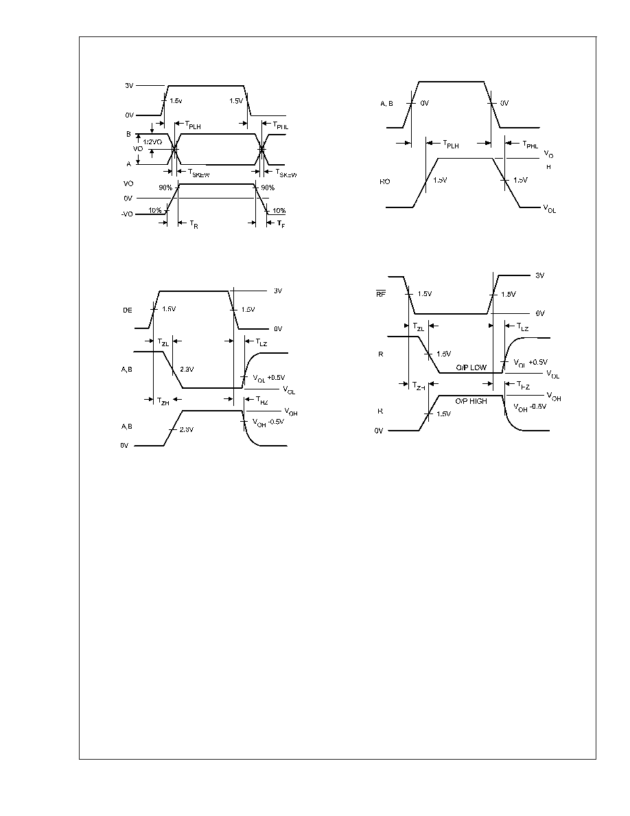
20086609
FIGURE 7. Driver Propagation Delay, Rise / Fall Time
20086610
FIGURE 8. Driver Enable / Disable Time
20086611
FIGURE 9. Receiver Propagation Delay
20086612
FIGURE 10. Receiver Enable / Disable Time
LMS485E
www.national.com
10
Application Information
POWER LINE NOISE FILTERING
A factor to consider in designing power and ground is noise
filtering. A noise filtering circuit is designed to prevent noise
generated by the integrated circuit (IC) as well as noise
entering the IC from other devices. A common filtering
method is to place by-pass capacitors (C
bp
) between the
power and ground lines.
Placing a by-pass capacitor (C
bp
) with the correct value at
the proper location solves many power supply noise prob-
lems. Choosing the correct capacitor value is based upon
the desired noise filtering range. Since capacitors are not
ideal, they may act more like inductors or resistors over a
specific frequency range. Thus, many times two by-pass
capacitors may be used to filter a wider bandwidth of noise.
It is highly recommended to place a larger capacitor, such as
10µF, between the power supply pin and ground to filter out
low frequencies and a 0.1µF to filter out high frequencies.
By-pass capacitors must be mounted as close as possible to
the IC to be effective. Longs leads produce higher imped-
ance at higher frequencies due to stray inductance. Thus,
this will reduce the by-pass capacitor's effectiveness. Sur-
face mounted chip capacitors are the best solution because
they have lower inductance.
20086622
FIGURE 11. Placement of by-pass Capacitors, C
bp
LMS485E
www.national.com
11
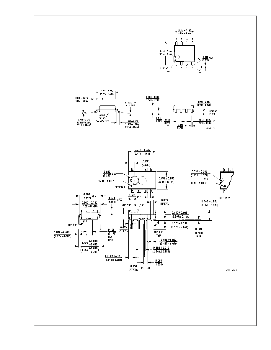
Physical Dimensions
inches (millimeters) unless otherwise noted
8-Pin SOIC
NS Package Number M08A
8-Pin DIP
NS Package Number N08E
LMS485E
www.national.com
12
Notes
LIFE SUPPORT POLICY
NATIONAL'S PRODUCTS ARE NOT AUTHORIZED FOR USE AS CRITICAL COMPONENTS IN LIFE SUPPORT
DEVICES OR SYSTEMS WITHOUT THE EXPRESS WRITTEN APPROVAL OF THE PRESIDENT AND GENERAL
COUNSEL OF NATIONAL SEMICONDUCTOR CORPORATION. As used herein:
1. Life support devices or systems are devices or
systems which, (a) are intended for surgical implant
into the body, or (b) support or sustain life, and
whose failure to perform when properly used in
accordance with instructions for use provided in the
labeling, can be reasonably expected to result in a
significant injury to the user.
2. A critical component is any component of a life
support device or system whose failure to perform
can be reasonably expected to cause the failure of
the life support device or system, or to affect its
safety or effectiveness.
BANNED SUBSTANCE COMPLIANCE
National Semiconductor certifies that the products and packing materials meet the provisions of the Customer Products
Stewardship Specification (CSP-9-111C2) and the Banned Substances and Materials of Interest Specification
(CSP-9-111S2) and contain no ``Banned Substances'' as defined in CSP-9-111S2.
National Semiconductor
Americas Customer
Support Center
Email: new.feedback@nsc.com
Tel: 1-800-272-9959
National Semiconductor
Europe Customer Support Center
Fax: +49 (0) 180-530 85 86
Email: europe.support@nsc.com
Deutsch Tel: +49 (0) 69 9508 6208
English
Tel: +44 (0) 870 24 0 2171
FranÁais Tel: +33 (0) 1 41 91 8790
National Semiconductor
Asia Pacific Customer
Support Center
Email: ap.support@nsc.com
National Semiconductor
Japan Customer Support Center
Fax: 81-3-5639-7507
Email: jpn.feedback@nsc.com
Tel: 81-3-5639-7560
www.national.com
LMS485E
Low
Power
RS-485
/
RS-422
Differential
Bus
T
ransceiver
National does not assume any responsibility for use of any circuitry described, no circuit patent licenses are implied and National reserves the right at any time without notice to change said circuitry and specifications.