 | –≠–ª–µ–∫—Ç—Ä–æ–Ω–Ω—ã–π –∫–æ–º–ø–æ–Ω–µ–Ω—Ç: LMV112SD | –°–∫–∞—á–∞—Ç—å:  PDF PDF  ZIP ZIP |
LMV112
40 MHz Dual Clock Buffer
General Description
The LMV112 is a high speed dual clock buffer designed for
portable communications and accurate multi-clock systems.
The LMV112 integrates two 40 MHz low noise buffers which
optimizes application and out performs large discrete solu-
tions. This device enables superb system operation between
the base band and the oscillator signal path while eliminating
crosstalk.
National Semiconductor's unique technology and design de-
liver accuracy, capacitance and load resistance while in-
creasing the drive capability of the device. The low power
consumption makes the LMV112 perfect for battery applica-
tions.
The robust, independent, and flexible buffers are designed to
provide the customer with the ability to manage complex
clock signals in the latest wireless applications. The buffers
deliver 110 V/µs internal slew rate with independent shut-
down and duty cycle precision. The patented analog circuit
drives capacitive loads beyond 20 pF. National's proven
biasing technique has 1V centering, rail-to-rail input/output
unity gain, and AC coupled convenient inputs. These inte-
grated cells save space and require no external bias resis-
tors. National's rapid recovery after disable optimizes perfor-
mance and current consumption. The LMV112 offers
individual enable pin controls and since there is no internal
ground reference either single or split supply configurations
offer additional system flexibility and power choices.
The LMV112 is a proven replacement for any discrete cir-
cuitry and simplifies board layout while minimizing related
parasitic components.
The LMV112 is produced in the small LLP package which
offers high quality while minimizing its use of PCB space.
National's advanced packaging offers direct PCB-IC evalu-
ation via pin access.
Features
(Typical values are: V
SUPPLY
= 2.7V and C
L
= 20 pF, unless
otherwise specified)
n
Small signal bandwidth
40 MHz
n
Supply voltage range
2.4V to 5V
n
Slew rate
110 V/µs
n
Total supply current
1.6 mA
n
Shutdown current
59 µA
n
Rail-to-rail input and output
n
Individual buffer enable pins
n
Rapid T
on
technology
n
Crosstalk rejection circuitry
n
8-pin LLP, pin access packaging
n
Temperature range
-40∞C to 85∞C
Applications
n
3G mobile applications
n
WLAN≠WiMAX modules
n
TD_SCDMA multi-mode MP3 and camera
n
GSM modules
n
Oscillator modules
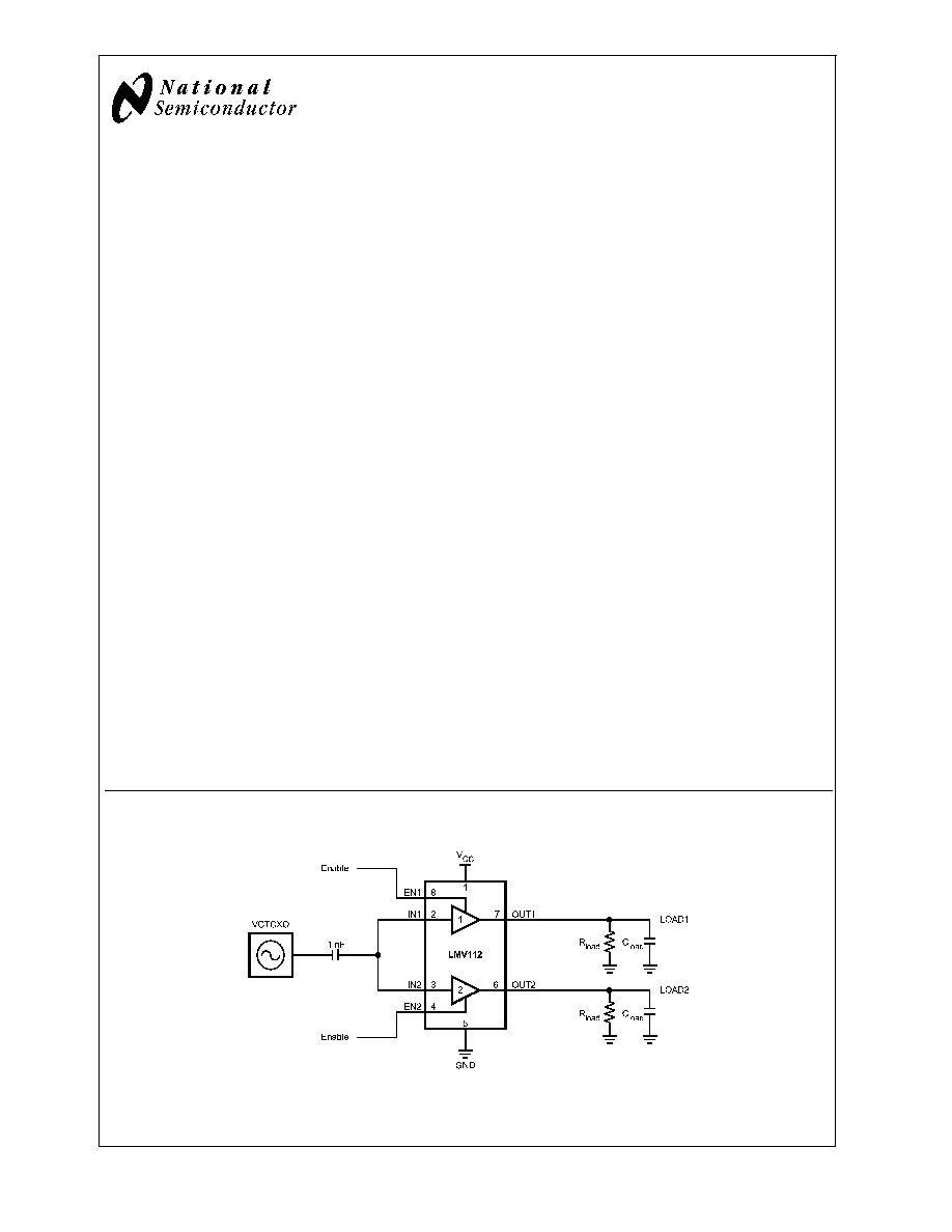
Typical Application
20135302
June 2005
LMV1
12
40
MHz
Dual
Clock
Buffer
© 2005 National Semiconductor Corporation
DS201353
www.national.com

Absolute Maximum Ratings
(Note 1)
If Military/Aerospace specified devices are required,
please contact the National Semiconductor Sales Office/
Distributors for availability and specifications.
Supply Voltages (V
+
≠ V
-
)
5.5V
ESD Tolerance (Note 2)
Human Body
2000V
Machine Model
200V
Storage Temperature Range
-65∞C to +150∞C
Junction Temperature (Note 3)
+150∞C
Soldering Information
Infrared or Convection (35 sec.)
235∞C
Operating Ratings
(Note 1)
Supply Voltage (V
+
≠ V
-
)
2.4V to 5.0V
Temperature Range (Notes 3, 4)
-40∞C to +85∞C
Package Thermal Resistance (Notes 3, 4)
LLP-8 (
JA
)
217∞C/W
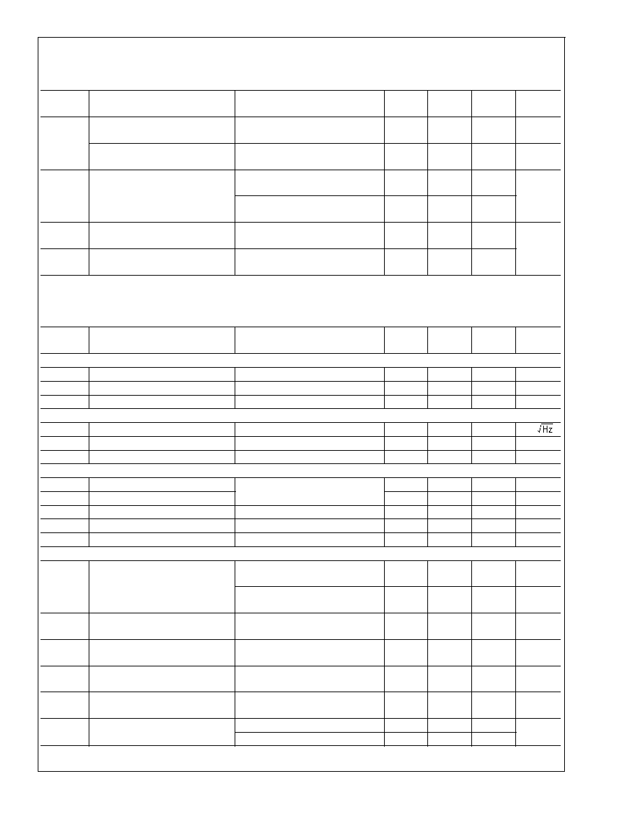
2.7V Electrical Characteristics
Unless otherwise specified, all limits are guaranteed for T
J
= 25∞C, V
DD
= 2.7V, V
SS
= 0V, V
CM
= 1V, Enable
1,2
= V
DD
, C
L
= 20
pF, R
L
= 30 k
, C
COUPLING
= 1 nF. Boldface limits apply at temperature range extremes of operating condition. See (Note 4)
Symbol
Parameter
Conditions
Min
(Note 6)
Typ
(Note 5)
Max
(Note 6)
Units
Frequency Domain Response
SSBW
Small Signal Bandwidth
V
IN
= 0.63 V
PP
; -3 dB
40
MHz
FPBW
Full Power Bandwidth
V
IN
= 1.6 V
PP
; -3 dB
28
MHz
GFN
Gain Flatness
<
0.1 dB
f
>
100 kHz
3.4
MHz
Distortion and Noise Performance
e
n
Input-Referred Voltage Noise
f = 1 MHz
26
nV/
I
SOLATION
Output to Input
f = 1 MHz
91
dB
CT
Crosstalk Rejection
f = 26 MHz, P
IN
= 0 dBm
54
dB
Time Domain Response
t
r
Rise Time
0.1 V
PP
Step (10-90%), f = 1 MHz
7
ns
t
f
Fall Time
6
ns
t
s
Settling Time to 0.1%
1 V
PP
Step, f = 1 MHz
118
ns
OS
Overshoot
0.1 V
PP
Step, f = 1 MHz
41
%
SR
Slew Rate (Note 7)
V
IN
= 1.6 V
PP
, f = 26 MHz
110
V/µs
Static DC Performance
I
S
Supply Current
Enable
1,2
= V
DD
; No Load
1.6
2.0
2.1
mA
Enable
1,2
= V
SS
; No Load
59
72
78
µA
PSRR
Power Supply Rejection Ratio
DC (3.0V to 5.0V)
58
57
68
dB
A
CL
Small Signal Voltage Gain
V
OUT
= 0.1 V
PP
0.97
0.95
1.01
1.05
1.07
V/V
V
OS
Output Offset Voltage
0.4
16
17
mV
TC V
OS
Temperature Coefficient Output
Offset Voltage (Note 8)
4
µV/∞C
R
OUT
Output Resistance
f = 100 kHz
0.5
f = 26 MHz
140
Miscellaneous Performance
R
IN
Input Resistance per Buffer
Enable = V
DD
141
k
Enable = V
SS
141
C
IN
Input Capacitance per Buffer
Enable = V
DD
2.3
pF
Enable = V
SS
2.3
Z
IN
Input Impedance
f = 26 MHz, Enable = V
DD
10.4
k
f = 26 MHz, Enable = V
SS
10.9
LMV1
12
www.national.com
2
2.7V Electrical Characteristics
(Continued)
Unless otherwise specified, all limits are guaranteed for T
J
= 25∞C, V
DD
= 2.7V, V
SS
= 0V, V
CM
= 1V, Enable
1,2
= V
DD
, C
L
= 20
pF, R
L
= 30 k
, C
COUPLING
= 1 nF. Boldface limits apply at temperature range extremes of operating condition. See (Note 4)
Symbol
Parameter
Conditions
Min
(Note 6)
Typ
(Note 5)
Max
(Note 6)
Units
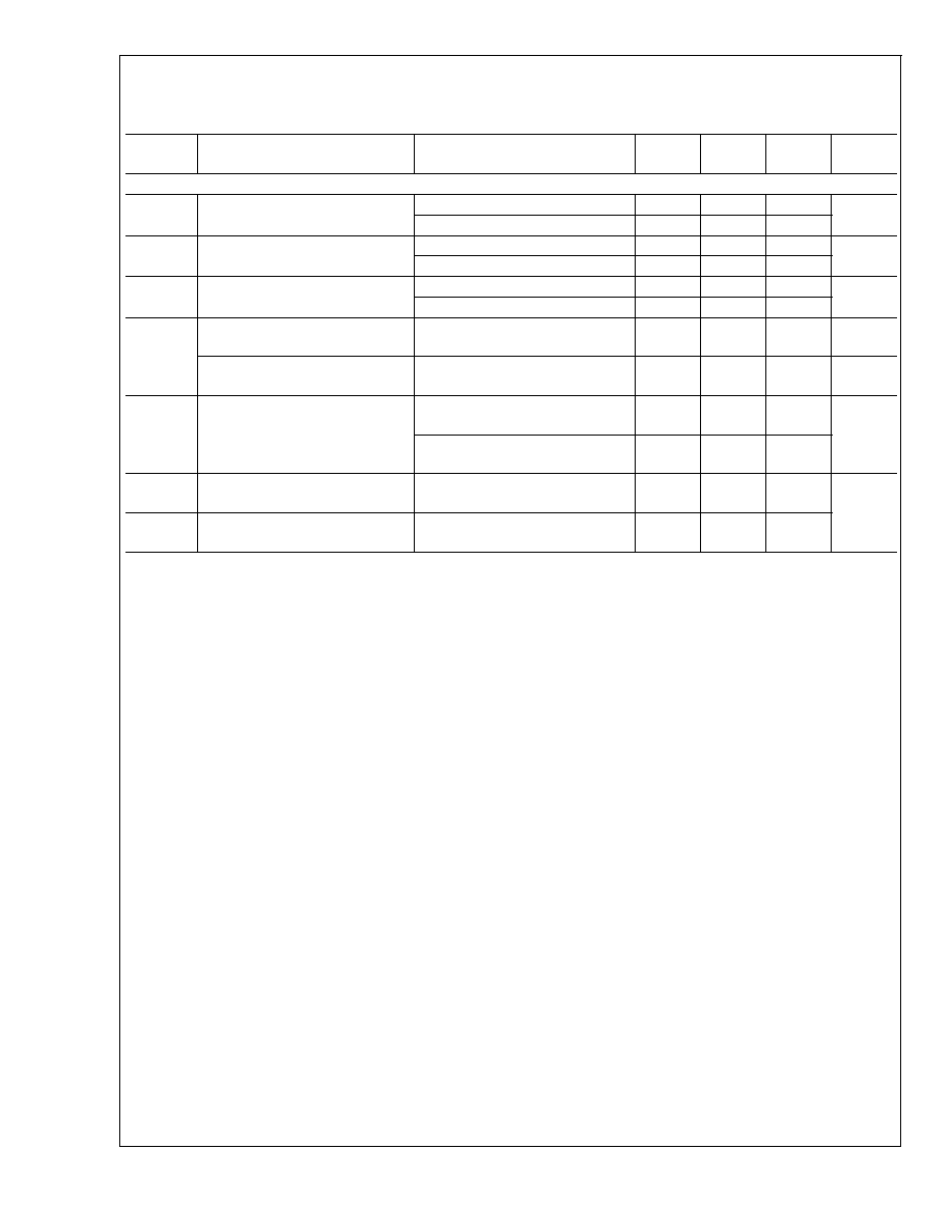
V
O
Output Swing Positive
V
IN
= V
DD
2.65
2.63
2.69
V
Output Swing Negative
V
IN
= V
SS
10
50
65
mV
I
SC
Output Short-Circuit Current
(Note 9)
Sourcing
-18
-13
-27
mA
Sinking
20
16
30
V
en_hmin
Enable High Active Minimum
Voltage
1.2
V
V
en_lmax
Enable Low Inactive Maximum
Voltage
0.6
5V Electrical Characteristics
Unless otherwise specified, all limits are guaranteed for T
J
= 25∞C, V
DD
= 5V, V
SS
= 0V, V
CM
= 1V, Enable
1,2
= V
DD
, C
L
= 20
pF, R
L
= 30 k
, C
COUPLING
= 1 nF. Boldface limits apply at temperature range extremes of operating condition. See (Note 4)
Symbol
Parameter
Conditions
Min
(Note 6)
Typ
(Note 5)
Max
(Note 6)
Units
Frequency Domain Response
SSBW
Small Signal Bandwidth
V
IN
= 0.63 V
PP
; -3 dB
42
MHz
FPBW
Full Power Bandwidth
V
IN
= 1.6 V
PP
; -3 dB
31
MHz
GFN
Gain Flatness
<
0.1 dB
f
>
100 kHz
4.9
MHz
Distortion and Noise Performance
e
n
Input-Referred Voltage Noise
f = 1 MHz
27
nV/
I
SOLATION
Output to Input
f = 1 MHz
90
dB
CT
Crosstalk Rejection
f = 26 MHz, P
IN
= 0 dBm
61
dB
Time Domain Response
t
r
Rise Time
0.1 V
PP
Step (10-90%), f = 1 MHz
7
ns
t
f
Fall Time
6
ns
t
s
Settling Time to 0.1%
1 V
PP
Step, f = 1 MHz
80
ns
OS
Overshoot
0.1V
PP
Step, f = 1 MHz
20
%
SR
Slew Rate (Note 7)
V
IN
= 1.6 V
PP
, f = 26 MHz
120
V/µs
Static DC Performance
I
S
Supply Current
Enable
1,2
= V
DD
; No Load
2.5
3.5
3.8
mA
Enable
1,2
= V
SS
; No Load
62
80
89
µA
PSRR
Power Supply Rejection Ratio
DC (3.0V to 5.0V)
58
57
68
dB
A
CL
Small Signal Voltage Gain
V
OUT
= 0.1 V
PP
0.99
0.97
1.00
1.01
1.03
V/V
V
OS
Output Offset Voltage
1.3
16
17
mV
TC V
OS
Temperature Coefficient Output
Offset Voltage (Note 8)
3
µV/∞C
R
OUT
Output Resistance
f = 100 kHz
0.5
f = 26 MHz
118
LMV1
12
www.national.com
3
5V Electrical Characteristics
(Continued)
Unless otherwise specified, all limits are guaranteed for T
J
= 25∞C, V
DD
= 5V, V
SS
= 0V, V
CM
= 1V, Enable
1,2
= V
DD
, C
L
= 20
pF, R
L
= 30 k
, C
COUPLING
= 1 nF. Boldface limits apply at temperature range extremes of operating condition. See (Note 4)
Symbol
Parameter
Conditions
Min
(Note 6)
Typ
(Note 5)
Max
(Note 6)
Units
Miscellaneous Performance
R
IN
Input Resistance per Buffer
Enable = V
DD
134
k
Enable = V
SS
134
C
IN
Input Capacitance per Buffer
Enable = V
DD
2.0
pF
Enable = V
SS
2.0
Z
IN
Input Impedance
f = 26 MHz, Enable = V
DD
7.2
k
f = 26 MHz, Enable = V
SS
8.0
V
O
Output Swing Positive
V
IN
= V
DD
4.96
4.94
4.99
V
Output Swing Negative
V
IN
= V
SS
10
40
55
mV
I
SC
Output Short-Circuit Current
(Note 9)
Sourcing
-40
-28
-68
mA
Sinking
70
50
98
V
en_hmin
Enable High Active Minimum
Voltage
1.2
V
V
en_lmax
Enable Low Inactive Maximum
Voltage
0.6
Note 1: Absolute Maximum Ratings indicate limits beyond which damage to the device may occur. Operating Ratings indicate conditions for which the device is
intended to be functional, but specific performance is not guaranteed. For guaranteed specifications and the test conditions, see the Electrical Characteristics Tables.
Note 2: Human Body Model: 1.5 k
in series with 100 pF. Machine Model: 0 in series with 200 pF.
Note 3: The maximum power dissipation is a function of T
J(MAX)
,
JA
, and T
A
. The maximum allowable power dissipation at any ambient temperature is
P
D
= (T
J(MAX)
- T
A
) /
JA
. All numbers apply for packages soldered directly onto a PC board.
Note 4: Electrical Table values apply only for factory testing conditions at the temperature indicated. Factory testing conditions result in very limited self-heating of
the device such that T
J
= T
A
. There is no guarantee of parametric performance as indicated in the electrical tables under conditions of internal self-heating where
T
J
>
T
A
.
Note 5: Typical Values represent the most likely parametric norm.
Note 6: All limits are guaranteed by testing or statistical analysis.
Note 7: Slew rate is the average of the positive and negative slew rate.
Note 8: Average Temperature Coefficient is determined by dividing the changing in a parameter at temperature extremes by the total temperature change.
Note 9: Short-Circuit test is a momentary test. Continuous short circuit operation at elevated ambient temperature can result in exceeding the maximum allowed
junction temperature of 150∞C.
LMV1
12
www.national.com
4
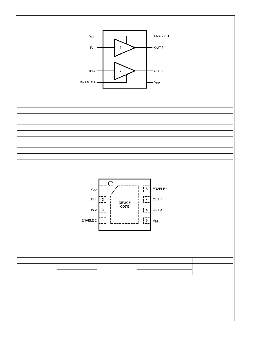
Block Diagram
20135301
Pin Description
Pin No.
Pin Name
Description
1
V
DD
Voltage supply connection
2
IN 1
Input 1
3
IN 2
Input 2
4
ENABLE 2
Enable buffer 2
5
V
SS
Ground connection
6
OUT 2
Output 2
7
OUT 1
Output 1
8
ENABLE 1
Enable buffer 1
Connection Diagram
8-Pin LLP
20135331
Top View
Ordering Information
Package
Part Number
Package Marking
Transport Media
NSC Drawing
8-Pin LLP
No Pull Back
LMV112SD
112SD
1k Units Tape and Reel
SDA08A
LMV112SDX
4.5k Units Tape and Reel
LMV1
12
www.national.com
5