 | –≠–ª–µ–∫—Ç—Ä–æ–Ω–Ω—ã–π –∫–æ–º–ø–æ–Ω–µ–Ω—Ç: LMV115MG | –°–∫–∞—á–∞—Ç—å:  PDF PDF  ZIP ZIP |
LMV115
GSM Baseband 30MHz 2.8V Oscillator Buffer
General Description
The LMV115 is a 30MHz buffer specially designed to mini-
mize the effects of spurious signals from the base band chip
to the oscillator. The buffer also minimizes the influence of
varying load resistance and capacitance to the oscillator and
increases the drive capability.
The input of the LMV115 is internally biased with two equal
resistors to the power supply rails. This allows AC coupling
on the input.
The LMV115 offers a shutdown function to optimize current
consumption. This shutdown function can also be used to
control the supply voltage of an external oscillator. The de-
vice is in shutdown mode when the shutdown pin is con-
nected to V
DD
.
The LMV115 comes in SC70-6 package. This space saving
product reduces components, improves clock signal and
allows ease of placement for the best form factor.
Features
(Typical 2.8V supply; values unless otherwise specified)
n
Low supply current: 0.3mA
n
2.5V to 3.3V supply
n
AC coupling possible without external bias resistors.
n
Includes shutdown function external oscillator
n
SC70-6 pin package 2.1 x 2mm
n
Operating Temperature Range -40∞C to 85∞C
Applications
n
Cellular phones
n
GSM Modules
n
Oscillator Modules
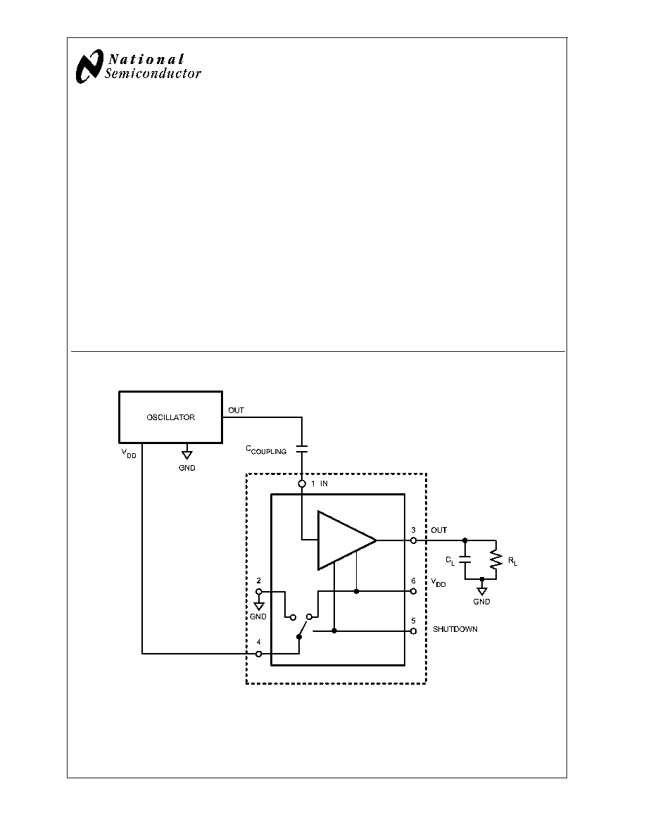
Schematic Diagram
20075129
December 2003
LMV1
15
GSM
Baseband
30MHz
2.8V
Oscillator
Buffer
© 2003 National Semiconductor Corporation
DS200751
www.national.com
Absolute Maximum Ratings
(Note 1)
If Military/Aerospace specified devices are required,
please contact the National Semiconductor Sales Office/
Distributors for availability and specifications.
ESD Tolerance
Human Body Model
2000V (Note 2)
Machine Model
150V (Note 3)
Supply Voltage (V
+
≠ V
-
)
3.6V
Output Short Circuit to V
+
(Note 4), (Note 5)
Output Short Circuit to V
-
(Note 4), (Note 5)
Storage Temperature Range
-65∞C to +150∞C
Junction Temperature (Note 6)
+150∞C
Mounting Temperature
Infrared or Convection (20 sec.)
235∞C
Operating Ratings
(Note 1)
Supply Voltage (V
+
≠ V
-
)
2.5V to 3.3V
Temperature Range (Note 6), (Note 7)
-40∞C to +85∞C
Package Thermal Resistance (Note 6), (Note 7)
SC70-6
414∞C/W
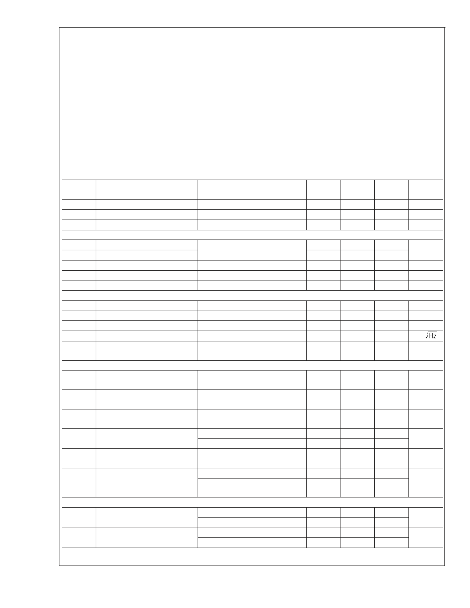
2.8V Electrical Characteristics
Unless otherwise specified, all limits guaranteed for T
J
= 25∞C, V
+
= 2.8V, V
-
= 0V, V
CM
= V
+
/2, shutdown = 0.0V, and R
L
=
50k
to V
+
/2, C
L
= 5pF to V
+
/2 and C
COUPLING
= 1nF.Boldface limits apply at the temperature extremes.
Symbol
Parameter
Conditions
Min
(Note 9)
Typ
(Note 8)
Max
(Note 9)
Units
SSBW
Small Signal Bandwidth
V
OUT
<
0.5V
PP
; -3dB
31
MHz
GFN
Gain Flatness
<
0.1dB
f
>
50kHz
2.8
MHz
FPBW
Full Power Bandwidth (-3dB)
V
OUT
= 1.0V
PP
(+4.5dBm)
9
MHz
Time Domain Response
t
r
Rise Time
0.1V
STEP
(10-90%)
11
ns
t
f
Fall Time
11
t
s
Settling Time to 0.1%
0.1V
STEP
95
ns
OS
Overshoot
0.1V
STEP
24
%
SR
Slew Rate
(Note 11)
18
V/µs
Distortion and Noise Performance
HD2
2
nd
Harmonic Distortion
V
OUT
= 500mV
PP
; f = 100kHz
-41
dBc
HD3
3
rd
Harmonic Distortion
V
OUT
= 500mV
PP
; f = 100kHz
-43
dBc
THD
Total Harmonic Distortion
V
OUT
= 500mV
PP
; f = 100kHz
-38
dBc
e
n
Input-Referred Voltage Noise
f = 1MHz
27
nV/
Isolation
Output to Input
See also Typical Performance
Characteristics
>
40
dB
Static DC Performance
A
CL
Small Signal Voltage Gain
V
OUT
= 100mV
PP
0.90
0.85
0.998
1.10
1.11
V/V
V
OS
Output Offset Voltage
3.5
35
55
mV
TC V
OS
Temperature Coefficient Output
Offset Voltage
(Note 12)
102
µV/∞C
R
OUT
Output Resistance
f = 10kHz
61
f = 25MHz
330
PSRR
Power Supply Rejection Ratio
V
+
= 2.8V to V
+
= 3.3V
41
38
42
dB
I
S
Supply Current
No Load; Shutdown = 2.8V
0.0
2.00
µA
No Load; Shutdown = 0V
314
450
520
Miscellaneous Performance
R
IN
Input Resistance
Shutdown = 2.8V
65
k
Shutdown = 0V
64
C
IN
Input Capacitance
Shutdown = 2.8V
1.82
pF
Shutdown = 0V
1.50
LMV1
15
www.national.com
2
2.8V Electrical Characteristics
(Continued)
Unless otherwise specified, all limits guaranteed for T
J
= 25∞C, V
+
= 2.8V, V
-
= 0V, V
CM
= V
+
/2, shutdown = 0.0V, and R
L
=
50k
to V
+
/2, C
L
= 5pF to V
+
/2 and C
COUPLING
= 1nF.Boldface limits apply at the temperature extremes.
Symbol
Parameter
Conditions
Min
(Note 9)
Typ
(Note 8)
Max
(Note 9)
Units
Z
IN
Input Impedance
f = 25MHz; Shutdown = 2.8V
2.38
k
f = 25MHz; Shutdown = 0V
2.47
V
O
Output Swing Positive
R
L
= 50k
to V
+
/2
1.90
1.65
2.16
V
Output Swing Negative
R
L
= 50k
to V
+
/2
1.05
1.35
1.30
I
O
Linear Output Current
No Load; V
OUT
= V
+
- 1.1V
(Sourcing)
-90
-35
-206
µA
No Load; V
OUT
= V
-
+ 1.1V
(Sinking)
100
50
205
I
SC
Output Short-Circuit Current
(Note 5)
No Load; Sourcing to V
+
/2
-90
-35
-186
µA
No Load; Sinking from V
+
/2
100
50
191
R
ON
Switch in ON Position
21
40
45
Note 1: Absolute Maximum Ratings indicate limits beyond which damage to the device may occur. Operating Ratings indicate conditions for which the device is
intended to be functional, but specific performance is not guaranteed. For guaranteed specifications and the test conditions, see the Electrical Characteristics.
Note 2: Human Body Model (HBM) is 1.5k
in series with 100pF.
Note 3: Machine Model, 0
in series with 200pF.
Note 4: Applies to both single-supply and split-supply operation. Continuous short circuit operation at elevated ambient temperature can result in exceeding the
maximum allowed junction temperature of 150∞C
Note 5: Infinite Duration; Short circuit test is a momentary test. See next note.
Note 6: The maximum power dissipation is a function of T
J(MAX)
,
JA
, and T
A
. The maximum allowable power dissipation at any ambient temperature is
P
D
= (T
J(MAX)
-T
A
) /
JA
. All numbers apply for packages soldered directly onto a PC board.
Note 7: Electrical Table values apply only for factory testing conditions at the temperature indicated. Factory testing conditions result in very limited self-heating of
the device such that T
J
= T
A
. There is no guarantee of parametric performance as indicated in the electrical tables under conditions of internal self-heating where
T
J
>
T
A
. See Applications section for information on temperature de-rating of this device.
Note 8: Typical Values represent the most likely parametric norm.
Note 9: All limits are guaranteed by testing or statistical analysis.
Note 10: Positive current corresponds to current flowing into the device.
Note 11: Slew rate is the average of the positive and negative slew rate.
Note 12: Average Temperature Coefficient is determined by dividing the change in a parameter at temperature extremes by the total temperature change.
LMV1
15
www.national.com
3
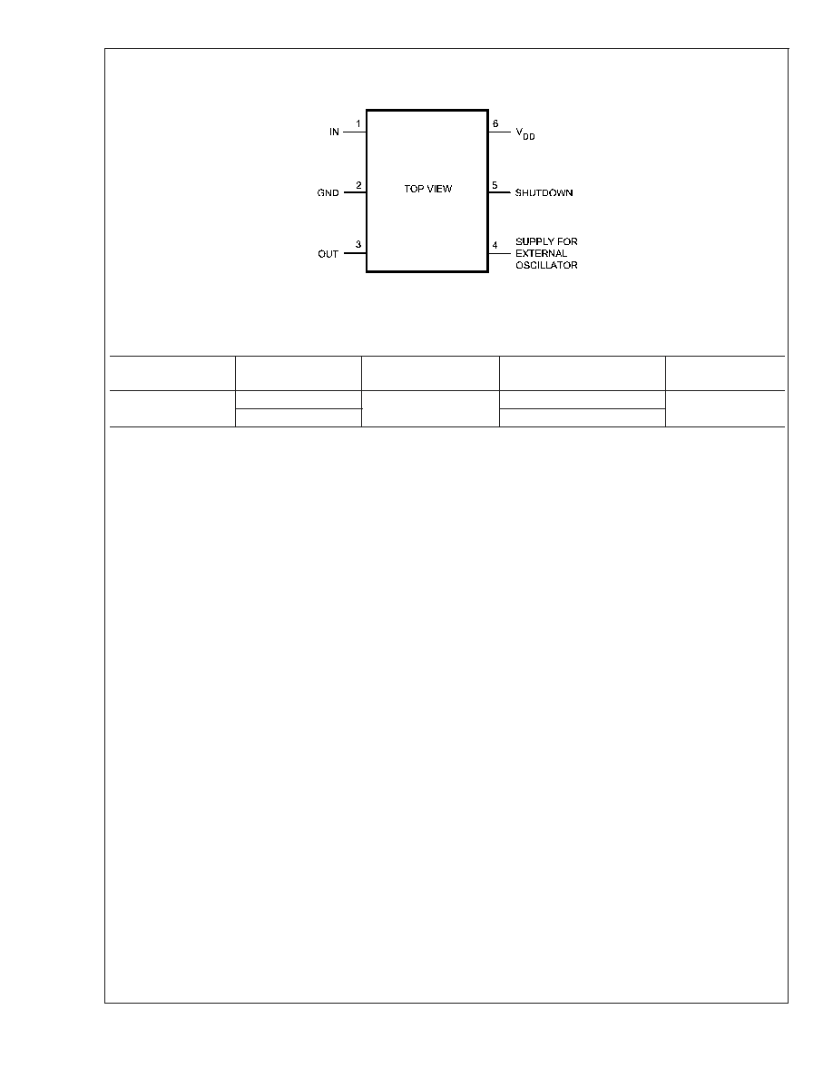
Connection Diagram
SC70-6
20075130
Top View
Ordering Information
Package
Part Number
Package Marking
Transport Media
NSC Drawing
SC70-6
LMV115MG
B04
250 Units Tape and Reel
MAA06A
LMV115MGX
3k Units Tape and Reel
LMV1
15
www.national.com
4

Typical Performance Characteristics
T
J
= 25∞C, V
+
= 2.8V, V
-
= 0V, V
CM
= V
+
/2, and R
L
, C
L
is
connected to V
+
/2; Unless otherwise specified.
Frequency and Phase Response
Frequency Response Over Temperature
20075103
20075104
Phase Response Over Temperature
Gain Flatness 0.1dB
20075114
20075106
Full Power Bandwidth
Transient Response Positive
20075105
20075119
LMV1
15
www.national.com
5