LMV2011
High Precision, Rail-to-Rail Output Operational Amplifier
General Description
The LMV2011 is a new precision amplifier that offers unprec-
edented accuracy and stability at an affordable price and is
offered in miniature (SOT23-5) package and in 8 lead SOIC
package. This device utilizes patented techniques to mea-
sure and continually correct the input offset error voltage.
The result is an amplifier which is ultra stable over time and
temperature. It has excellent CMRR and PSRR ratings, and
does not exhibit the familiar 1/f voltage and current noise
increase that plagues traditional amplifiers. The combination
of the LMV2011 characteristics makes it a good choice for
transducer amplifiers, high gain configurations, ADC buffer
amplifiers, DAC I-V conversion, and any other 2.7V-5V ap-
plication requiring precision and long term stability.
Other useful benefits of the LMV2011 are rail-to-rail output, a
low supply current of 930µA, and wide gain-bandwidth prod-
uct of 3MHz. These extremely versatile features found in the
LMV2011 provide high performance and ease of use.
Features
(For Vs = 5V, Typical unless otherwise noted)
n
Low Guaranteed V
os
over temperature
35µV
n
Low Noise with no 1/f
35nV/
n
High CMRR
130dB
n
High PSRR
120dB
n
High A
VOL
130dB
n
Wide gain-bandwidth product
3MHz
n
High slew rate
4V/µs
n
Low supply current
930µA
n
Rail-to-rail output
30mV
n
No external capacitors required
Applications
n
Precision Instrumentation Amplifiers
n
Thermocouple Amplifiers
n
Strain Gauge Bridge Amplifier
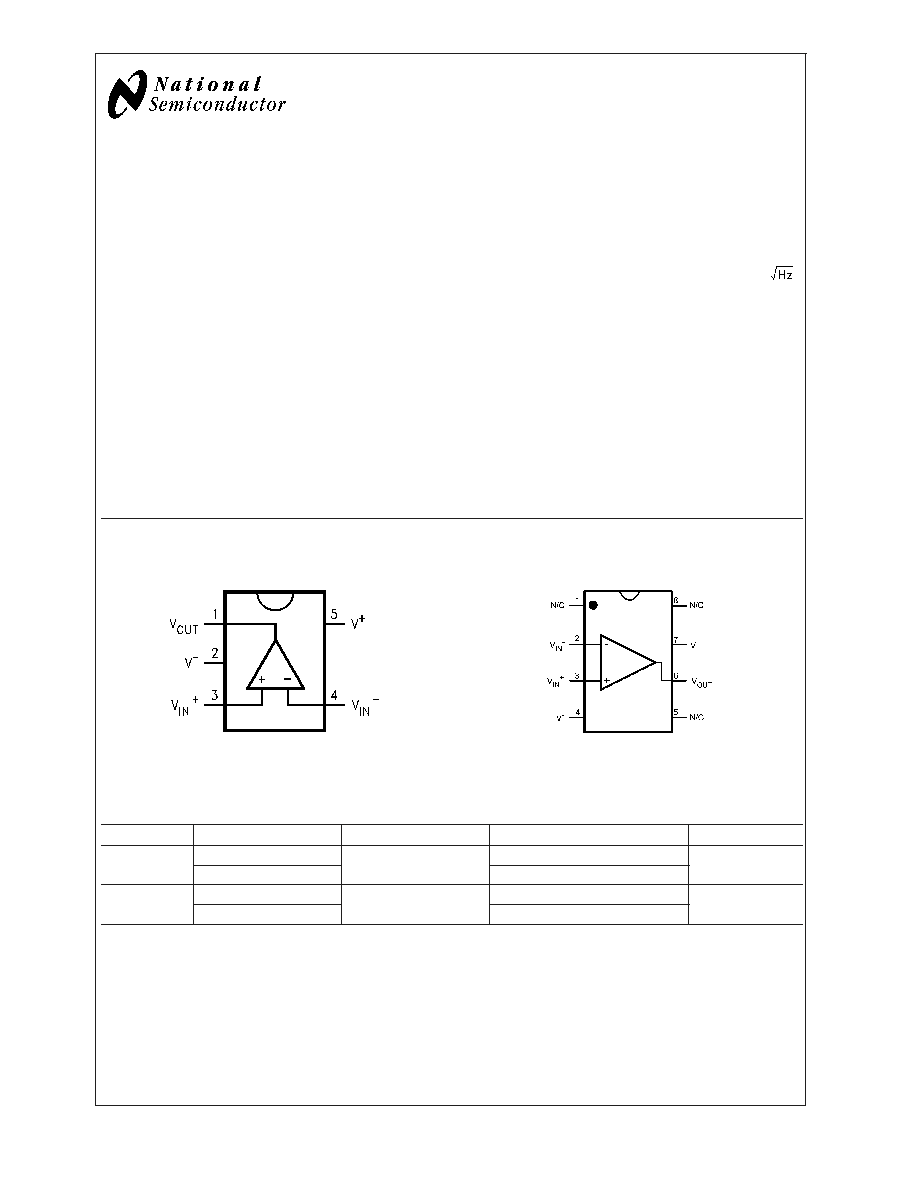
Connection Diagrams
5-Pin SOT23
8-Pin SOIC
20051502
Top View
20051538
Top View
Ordering Information
Package
Part Number
Package Marking
Transport Media
NSC Drawing
5-Pin SOT23
LMV2011MF
A84A
1k Units Tape and Reel
MF05A
LMV2011MFX
3k Units Tape and Reel
8-Pin SOIC
LMV2011MA
LMV2011MA
95 Units/Rail
M08A
LMV2011MAX
2.5k Units Tape and Reel
April 2004
LMV201
1
High
Precision,
Rail-to-Rail
Output
Operational
Amplifier
© 2004 National Semiconductor Corporation
DS200515
www.national.com
Absolute Maximum Ratings
(Note 1)
If Military/Aerospace specified devices are required,
please contact the National Semiconductor Sales Office/
Distributors for availability and specifications.
ESD Tolerance
Human Body Model
2000V
Machine Model
200V
Supply Voltage
5.5V
Common-Mode Input Voltage
-0.3
V
CM
V
CC
+0.3V
Differential Input Voltage
±
Supply Voltage
Current At Input Pin
30mA
Current At Output Pin
30mA
Current At Power Supply Pin
50mA
Junction Temperature (T
J
)
150∞C
Lead Temperature (soldering
10 sec.)
+300∞C
Operating Ratings
(Note 1)
Supply Voltage
2.7V to 5.25V
Storage Temperature Range
-65∞C to 150∞C
Operating Temperature Range
0∞C to 70∞C
2.7V DC Electrical Characteristics
Unless otherwise specified, all limits guaranteed for T
J
= 25∞C, V
+
= 2.7V, V
-
= 0V, V
CM
= 1.35V, V
O
= 1.35V and R
L
>
1M
. Boldface limits apply at the temperature extremes.
Symbol
Parameter
Conditions
Min
Typ
Max
Units
V
OS
Input Offset Voltage
0.8
25
35
µV
Offset Calibration Time
0.5
10
12
ms
TCV
OS
Input Offset Voltage
0.015
µV/∞C
Long-Term Offset Drift
0.006
µV/month
Lifetime V
OS
Drift
2.5
5
µV
I
IN
Input Current
-3
pA
I
OS
Input Offset Current
6
pA
R
IND
Input Differential Resistance
9
M
CMRR
Common Mode Rejection
Ratio
-0.3
V
CM
0.9V
0
V
CM
0.9V
130
95
90
dB
PSRR
Power Supply Rejection
Ratio
2.7V
V
+
5V
120
95
90
dB
A
VOL
Open Loop Voltage Gain
R
L
= 10k
130
95
90
dB
R
L
= 2k
124
90
85
V
O
Output Swing
R
L
= 10k
to 1.35V
V
IN
(diff) =
±
0.5V
2.665
2.655
2.68
V
0.033
0.060
0.075
R
L
= 2k
to 1.35V
V
IN
(diff) =
±
0.5V
2.630
2.615
2.65
V
0.061
0.085
0.105
I
O
Output Current
Sourcing, V
O
= 0V
V
IN
(diff) =
±
0.5V
12
5
3
mA
Sinking, V
O
= 5V
V
IN
(diff) =
±
0.5V
18
5
3
R
OUT
Output Impedance
0.05
I
S
Supply Current
0.919
1.20
1.50
mA
LMV201
1
www.national.com
2
2.7V AC Electrical Characteristics
T
J
= 25∞C, V
+
= 2.7V, V
-
= 0V, V
CM
= 1.35V, V
O
= 1.35V, and R
L
>
1M
. Boldface limits apply at the temperature extremes.
Symbol
Parameter
Conditions
Min
Typ
Max
Units
GBW
Gain-Bandwidth Product
3
MHz
SR
Slew Rate
4
V/µs
m
Phase Margin
60
Deg
G
m
Gain Margin
-14
dB
e
n
Input-Referred Voltage
Noise
35
nV/
i
n
Input-Referred Current
Noise
150
fA/
e
n
p-p
Input-Referred Voltage
Noise
R
S
= 100
, DC to 10Hz
850
nV
pp
t
rec
Input Overload Recovery
Time
50
ms
t
s
Output Settling Time
A
V
= -1, R
L
= 2k
1V Step
1%
0.9
µs
0.1%
49
0.01%
100
5V DC Electrical Characteristics
Unless otherwise specified, all limits guaranteed for T
J
= 25∞C, V
+
=
5V, V
-
= 0V, V
CM
= 2.5V, V
O
= 2.5V and R
L
>
1M
. Boldface limits apply at the temperature extremes.
Symbol
Parameter
Conditions
Min
Typ
Max
Units
V
OS
Input Offset Voltage
0.12
25
35
µV
Offset Calibration Time
0.5
10
12
ms
TCV
OS
Input Offset Voltage
0.015
µV/∞C
Long-Term Offset Drift
0.006
µV/month
Lifetime V
OS
Drift
2.5
5
µV
I
IN
Input Current
-3
pA
I
OS
Input Offset Current
6
pA
R
IND
Input Differential Resistance
9
M
CMRR
Common Mode Rejection
Ratio
-0.3
V
CM
3.2
0
V
CM
3.2
130
100
90
dB
PSRR
Power Supply Rejection
Ratio
2.7V
V
+
5V
120
95
90
dB
A
VOL
Open Loop Voltage Gain
R
L
= 10k
130
105
100
dB
R
L
= 2k
132
95
90
V
O
Output Swing
R
L
= 10k
to 2.5V
V
IN
(diff) =
±
0.5V
4.96
4.95
4.978
V
0.040
0.070
0.085
R
L
= 2k
to 2.5V
V
IN
(diff) =
±
0.5V
4.895
4.875
4.919
V
0.091
0.115
0.140
I
O
Output Current
Sourcing, V
O
= 0V
V
IN
(diff) =
±
0.5V
15
8
6
mA
Sinking, V
O
= 5V
V
IN
(diff) =
±
0.5V
17
8
6
LMV201
1
www.national.com
3
5V DC Electrical Characteristics
Unless otherwise specified, all limits guaranteed for T
J
= 25∞C, V
+
=
5V, V
-
= 0V, V
CM
= 2.5V, V
O
= 2.5V and R
L
>
1M
. Boldface limits apply at the temperature extremes. (Continued)
Symbol
Parameter
Conditions
Min
Typ
Max
Units
R
OUT
Output Impedance
0.05
I
S
Supply Current per Channel
0.930
1.20
1.50
mA
5V AC Electrical Characteristics
T
J
= 25∞C, V
+
= 5V, V
-
= 0V, V
CM
= 2.5V, V
O
= 2.5V, and R
L
>
1M
. Boldface limits apply at the temperature extremes.
Symbol
Parameter
Conditions
Min
Typ
Max
Units
GBW
Gain-Bandwidth Product
3
MHz
SR
Slew Rate
4
V/µs
m
Phase Margin
60
deg
G
m
Gain Margin
-15
dB
e
n
Input-Referred Voltage
Noise
35
nV/
i
n
Input-Referred Current
Noise
150
fA/
e
n
p-p
Input-Referred Voltage
Noise
R
S
= 100
, DC to 10Hz
850
nV
pp
t
rec
Input Overload Recovery
Time
50
ms
t
s
Output Settling Time
A
V
= -1, R
L
= 2k
1V Step
1%
0.8
us
0.1%
36
0.01%
100
Note 1: Absolute Maximum Ratings indicate limits beyond which damage may occur. Operating Ratings indicate conditions for which the device is intended to be
functional, but specific performance is not guaranteed. For guaranteed specifications and test conditions, see the Electrical Characteristics.
LMV201
1
www.national.com
4
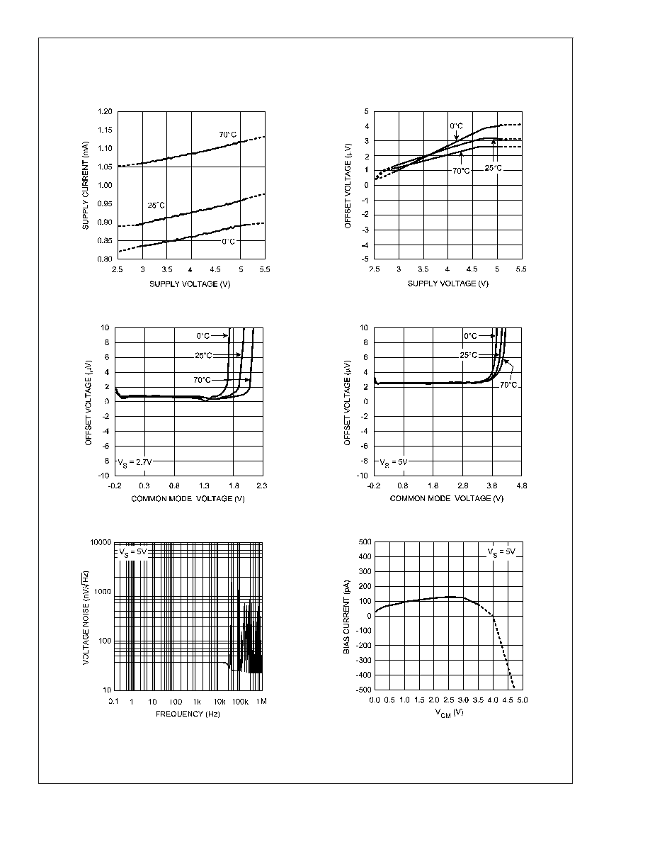
Typical Performance Characteristics
T
A
=25C, V
S
= 5V unless otherwise specified.
Supply Current vs. Supply Voltage
Offset Voltage vs. Supply Voltage
20051524
20051525
Offset Voltage vs. Common Mode
Offset Voltage vs. Common Mode
20051535
20051534
Voltage Noise vs. Frequency
Input Bias Current vs. Common Mode
20051504
20051503
LMV201
1
www.national.com
5