 | –≠–ª–µ–∫—Ç—Ä–æ–Ω–Ω—ã–π –∫–æ–º–ø–æ–Ω–µ–Ω—Ç: LMV248 | –°–∫–∞—á–∞—Ç—å:  PDF PDF  ZIP ZIP |
LMV248
Dual Band GSM Power Controller
General Description
The LMV248 RF power amplifier controller allows simple
implementation of transmit power control loops in GSM and
DCS/PCS and mobile phones. The LMV248 supports, GaAs
HBT and bipolar RF power amplifiers. The device operates
from a single supply of 2.5V to 5V. The LMV248 includes an
error amplifier with an input summing network, input and
output band switches, input filters, and output drivers. Ana-
log input signals processed are:
≠
Coupler/detector voltages from GSM and PCN band
power amplifier outputs.
≠
Base band DAC ramp signal.
≠
Temperature compensation diode voltages.
≠
Pre-bias voltage for faster PA control.
Selection of the GSM or PCN output driver is made using the
GSM/PCN band select pin.
The On/OFF pin allows rapid power up or shutdown of the
device during Tx or Rx slots. In the off mode, both output
drivers are set low for PA shutdown. In the on mode, the
non-active driver will remain low for continued PA shutdown.
A single external capacitor/resistor combination is used to
adjust the closed loop frequency response.
The LMV248 replaces multiple discrete parts, reducing
board area and cost. The LLP leadless package minimizes
board footprint and permits flexible optimized PCB place-
ment.
Features
n
Multi-band cellular operation (example: GSM, PCN)
n
Support of GaAs HBT and bipolar technology
n
Shutdown mode for power save in Rx slot (0.15µA)
n
Integrated ramp filter
n
Built-in current source for biasing Schottky diodes
n
Pre-biasing of PA control gate voltage (V
HOME
)
n
GPRS compliant
n
External loop compensation
n
Detector diode temperature compensation
n
Miniature packaging: LLP-16: 4mm x 4mm x 0.8mm
Applications
n
GSM mobile phone
n
TDMA RF control
n
Wireless LAN
n
PC and PDA modules
n
GPS navigation modules
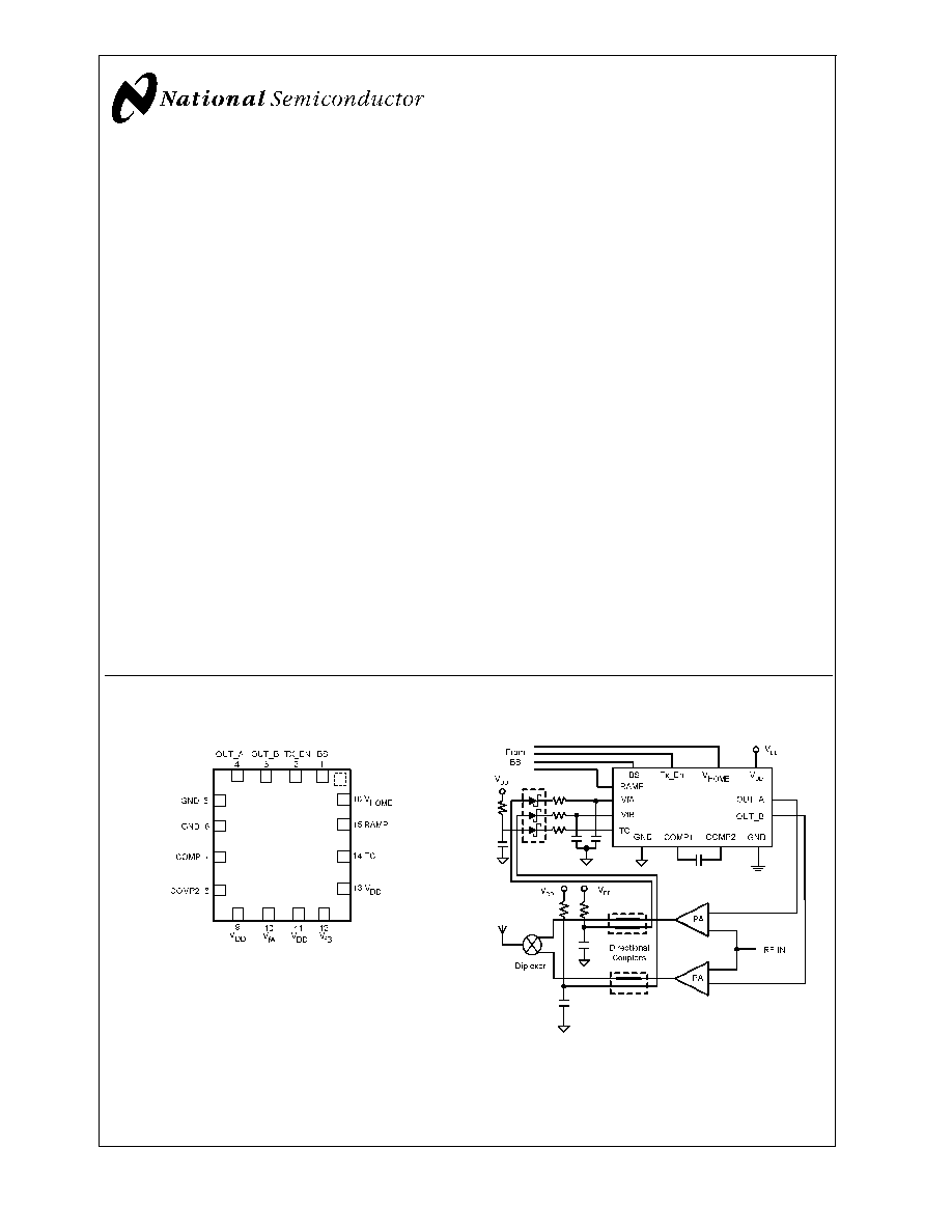
Connection Diagram
16-Pin LLP
10137201
Top View
Typical Application Circuit
10137202
FIGURE 1.
September 2001
LMV248
Dual
Band
GSM
Power
Controller
© 2001 National Semiconductor Corporation
DS101372
www.national.com
Absolute Maximum Ratings
(Note 1)
If Military/Aerospace specified devices are required,
please contact the National Semiconductor Sales Office/
Distributors for availability and specifications.
ESD Tolerance
Human Body Model (Note 1)
1500V
Machine Model
100V
Supply Voltage
V
DD
to GND
5.5V
Input Voltage Range
VfA, VfB, or TC to GND
10V
Ramp
0 to V
DD
V
HOME
0 to V
DD
Junction Temperature
150∞C max
Operating Temperature
-40∞C
<
T
J
<
85∞C
Storage Temperature Range
-65∞C to 150∞C
Lead Temperature (solder, 4
sec)
260∞C
Operating Ratings
(Note 1)
Supply Voltage
V
DD
to GND
2.5V to 5V
Input Voltage
VfA, VfB, or TC to V
DD
0V to 5V
Ramp
0.2V to 1.8V
V
HOME
0V to 2V
Temperature Range
-20∞C
T
J
85∞C
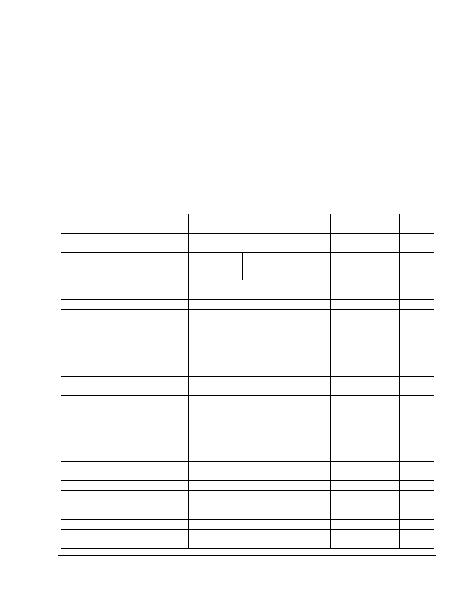
DC and AC Electrical Characteristics
Unless otherwise specified, all limits guaranteed for V
DD
= 2.8V, GND = 0V, T
J
= 25∞C. Boldface limits apply at temperature
range extremes of operating conditions.
Symbol
Parameter
Condition
Min
(Note 7)
Typ
(Note 8)
Max
(Note 7)
Units
V
OUT
A, B
Positive Output Voltage Swing
A, B
Sourcing 6mA, Tx_En = High
(Note 3)
2.6
2.7
V
V
OUT
A, B
Negative Output Voltage
Swing A, B
Sinking 2mA,
Tx_En = High
(Note 3,4,5)
V
HOME
= 0V
0.075
0.15
V
V
OUT
A, B
Negative Output Voltage
Swing A,B
Sinking 2mA, TX_EN = Low
(Note 3,4,5)
0.06
0.15
V
V
OS
Input Offset Voltage
(Note 6)
60
80
100
mV
BW
Bandwidth (-3dB)
Rf = 50k, No External Frequency
Compensation
>
1
MHz
SR
Output Slew Rate
No External Frequency
Compensation, V
HOME
= 0V
3
5.5
V/µs
I
VHOME
Current into V
HOME
Pin
(Note 7)
<
5
µA
I
BS
Current into BS Pin
(Note 7)
<
5
µA
I
Tx_En
Current into En Pin
(Note 7)
<
5
µA
I
VfA
I
VfB
Forward Bias Current Sources
(Note 7)
7
10
13
µA
I
TC
Temperature Compensation
Current Source
(Note 7)
7
10
13
µA
I
Vf-TC
Match
Current Source Matching
I
TC
/I
VfA
I
TC
/I
VfB
(Note 7)
±
2%
±
12%
V
LOW
BS or Tx_En Logic Low Input
Level
(Note 7)
0.8
V
V
HIGH
BS or Tx_En Logic High Input
Level
(Note 7)
1.8
V
I
SD
Supply Current in Shutdown
Tx_En = 0V
0.15
<
5
µA
V
RD
Vramp Deadband
(Note 7)
160
200
mV
t
d: Tx_En
Output Delay: Tx_En to
Output
3.5
6
µs
I
DD
Positive Supply Current
V
OUT
= V
DD/2
(Note 6)
1.1
1.8
mA
V
OUT
A,B
Threshold Select Voltages
Tx_En = High, V
HOME
= 2V
(Note 3, 4, and 5)
1.60
2
2.40
V
LMV248
www.national.com
2
DC and AC Electrical Characteristics
(Continued)
Note 1: Absolute Maximum Ratings indicate limits beyond which damage to the device may occur. Operating Ratings indicate conditions for which the device is
intended to be functional, but specific performance is not guaranteed. For guaranteed specifications and the test conditions, see the Electrical Characteristics.
Note 2: Human Body Model (HBM) is 1.5k
in series with 100pF.
Note 3: The output is not short circuit protected internally. External protection is necessary to prevent overheating and destruction or adverse reliability.
Note 4: Transients and spikes during V
DD
on transition are allowed only as described in the diagram.
Note 5: No overshoot above 100mV occurs when Tx_En is switched high to low or low to high. The overshoot is influenced by the external compensation capacitor.
Note 6: Tested in closed loop configuration.
Note 7: All limits are guaranteed by design or statistical analysis.
Note 8: Typical values represent the most likely parametric norm.
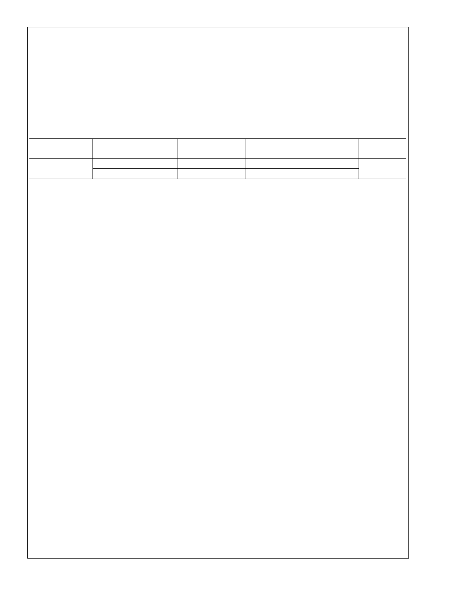
Ordering Information
Package
Part Number
Packaging Marking
Transport Media
NSC
Drawing
16-Pin LLP
LMV248LQ
LMV248
1k Units Tape and Reel
LQA16A
LMV248LQX
LMV248
4.5k Units Tape and Reel
LMV248
www.national.com
3
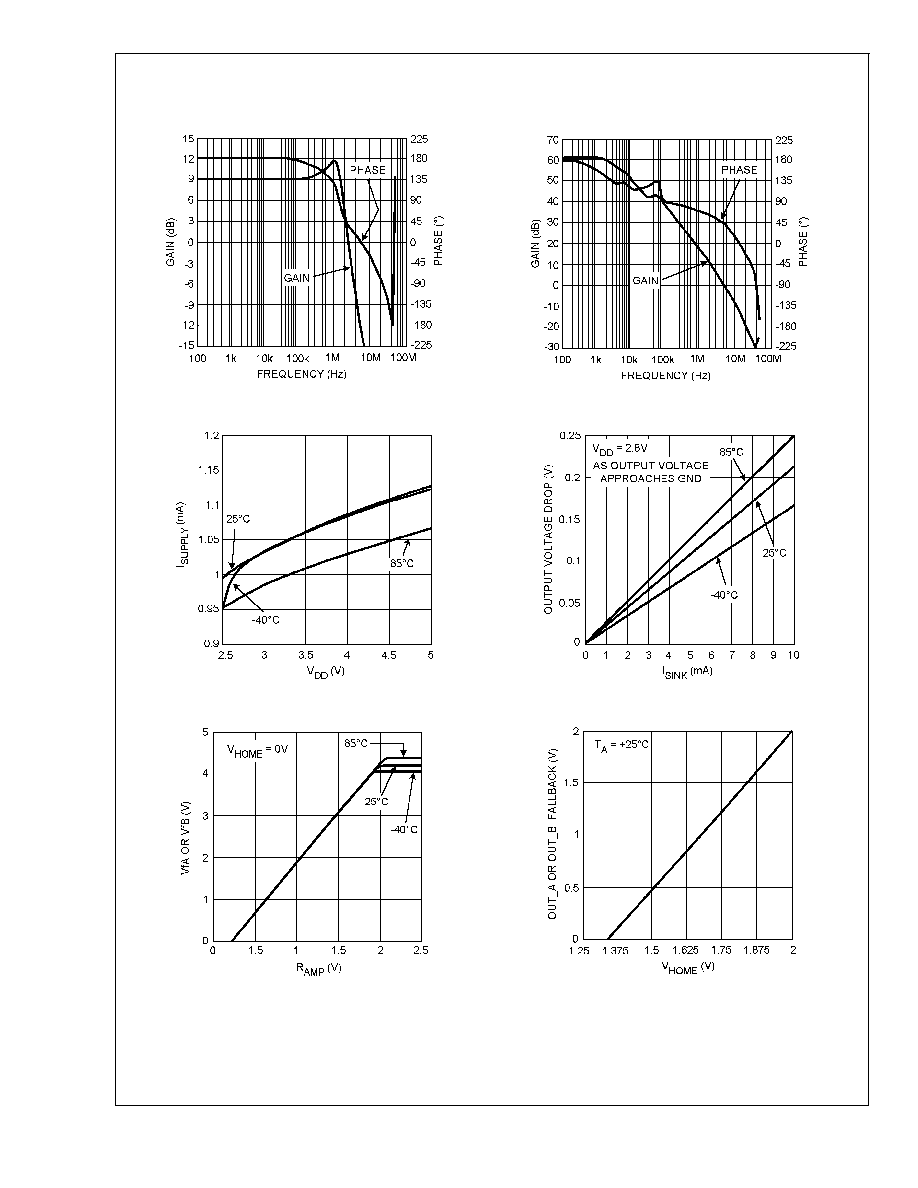
Typical Performance Characteristics
Error Amp Closed Loop Gain and Phase
(Rf = R
COMP
= 137k, A
V
-2.8)
Error Amp Open Loop Gain and Phase
(Rf = R
COMP
= 137k, A
V
-2.8)
10137203
10137204
I
SUPPLY
vs. V
DD
Voltage Drop (Sinking)
10137205
10137206
VfA or VfB vs. Ramp
Output Fallback Voltage Out A or Out B vs. V
HOME
10137207
10137208
LMV248
www.national.com
4
Typical Performance
Characteristics
(Continued)
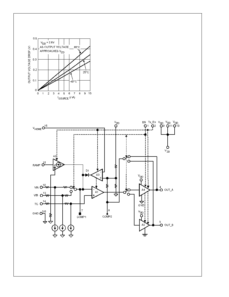
Voltage Drop (Sourcing)
10137209
Block Diagram
10137210
FIGURE 2.
LMV248
www.national.com
5