 | –≠–ª–µ–∫—Ç—Ä–æ–Ω–Ω—ã–π –∫–æ–º–ø–æ–Ω–µ–Ω—Ç: LP2953MDS | –°–∫–∞—á–∞—Ç—å:  PDF PDF  ZIP ZIP |
LP2952/LP2952A/LP2953/LP2953A
Adjustable Micropower Low-Dropout Voltage Regulators
General Description
The LP2952 and LP2953 are micropower voltage regulators
with very low quiescent current (130 µA typical at 1 mA load)
and very low dropout voltage (typ. 60 mV at light load and
470 mV at 250 mA load current). They are ideally suited for
battery-powered systems. Furthermore, the quiescent cur-
rent increases only slightly at dropout, which prolongs bat-
tery life.
The LP2952 and LP2953 retain all the desirable characteris-
tics of the LP2951, but offer increased output current, addi-
tional features, and an improved shutdown function.
The internal crowbar pulls the output down quickly when the
shutdown is activated.
The error flag goes low if the output voltage drops out of
regulation.
Reverse battery protection is provided.
The internal voltage reference is made available for external
use, providing a low-T.C. reference with very good line and
load regulation.
The parts are available in DIP and surface mount packages.
Features
n
Output voltage adjusts from 1.23V to 29V
n
Guaranteed 250 mA output current
n
Extremely low quiescent current
n
Low dropout voltage
n
Extremely tight line and load regulation
n
Very low temperature coefficient
n
Current and thermal limiting
n
Reverse battery protection
n
50 mA (typical) output pulldown crowbar
n
5V and 3.3V versions available
LP2953 Versions Only
n
Auxiliary comparator included with CMOS/TTL
compatible output levels. Can be used for fault
detection, low input line detection, etc.
Applications
n
High-efficiency linear regulator
n
Regulator with under-voltage shutdown
n
Low dropout battery-powered regulator
n
Snap-ON/Snap-OFF regulator
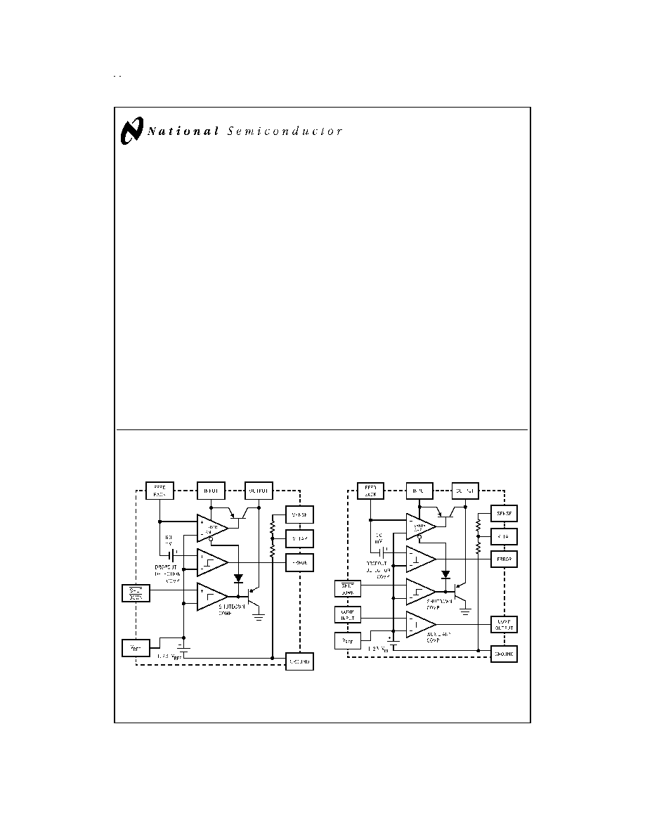
Block Diagrams
LP2952
DS011127-1
LP2953
DS011127-2
May 1999
LP2952/LP2952A/LP2953/LP2953A
Adjustable
Micropower
Low-Dropout
V
oltage
Regulators
© 1999 National Semiconductor Corporation
DS011127
www.national.com
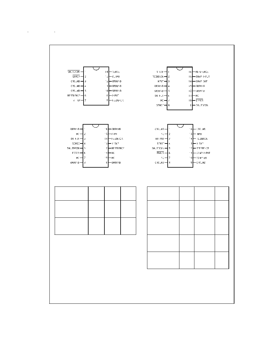
Pinout Drawings
Ordering Information
LP2952
Order
Number
Temp.
Range
(T
J
) ∞C
Package
NSC
Drawing
Number
LP2952IN,
LP2952AIN,
LP2952IN-3.3,
LP2952AIN-3.3
-40 to
+125
14-Pin
Molded
DIP
N14A
LP2952IM,
LP2952AIM,
LP2952IM-3.3,
LP2952AIM-3.3
-40 to
+125
16-Pin
Surface
Mount
M16A
LP2953
Order
Number
Temp.
Range
(T
J
) ∞C
Package
NSC
Drawing
Number
LP2953IN,
LP2953AIN,
LP2953IN-3.3,
LP2953AIN-3.3
-40 to
+125
16-Pin
Molded DIP
N16A
LP2953IM,
LP2953AIM,
LP2953IM-3.3,
LP2953AIM-3.3
-40 to
+125
16-Pin
Surface
Mount
M16A
LP2953AMJ/883
5962-9233601MEA
LP2953AMJ-QMLV
5962-9233601VEA
-55 to
+150
16-Pin
Ceramic
DIP
J16A
LP2953AMWG/883
5962-9233601QXA
LP2953AMWG-QMLV
5962-9233601VXA
-55 to
+150
16-Pin
Ceramic
Surface
Mount
WG16A
LP2952
14-Pin DIP
DS011127-11
LP2953
16-Pin DIP
DS011127-13
LP2952
16-Pin SO
DS011127-12
LP2953
16-Pin SO
DS011127-14
www.national.com
2
Absolute Maximum Ratings
(Note 1)
If Military/Aerospace specified devices are required,
please contact the National Semiconductor Sales Office/
Distributors for availability and specifications.
Storage Temperature Range
-65∞C
T
A
+150∞C
Operating Temperature Range
LP2952I, LP2953I, LP2952AI,
LP2953AI, LP2952I-3.3,
LP2953I-3.3, LP2952AI-3.3,
LP2953AI-3.3
-40∞C
T
J
+125∞C
LP2953AM
-55∞C
T
A
+125∞C
Lead Temp. (Soldering, 5 seconds)
260∞C
Power Dissipation (Note 2)
Internally Limited
Maximum Junction Temperature
LP2952I, LP2953I, LP2952AI,
LP2953AI, LP2952I-3.3,
LP2953I-3.3, LP2952AI-3.3,
LP2953AI-3.3
+125∞C
LP2953AM
+150∞C
Input Supply Voltage
-20V to +30V
Feedback Input Voltage (Note 3)
-0.3V to +5V
Comparator Input Voltage (Note 4)
-0.3V to +30V
Shutdown Input Voltage (Note 4)
-0.3V to +30V
Comparator Output Voltage (Note 4)
-0.3V to +30V
ESD Rating (Note 15)
2 kV
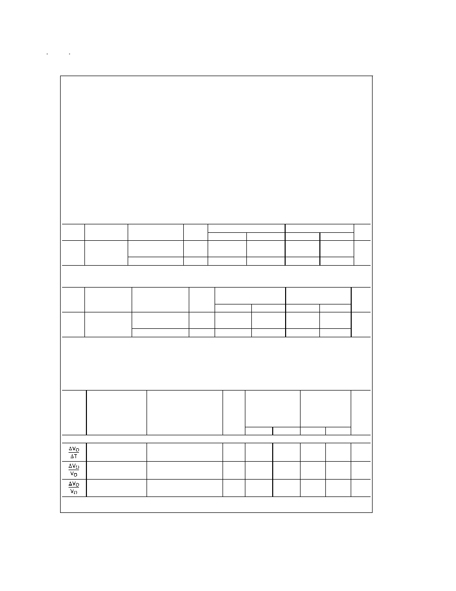
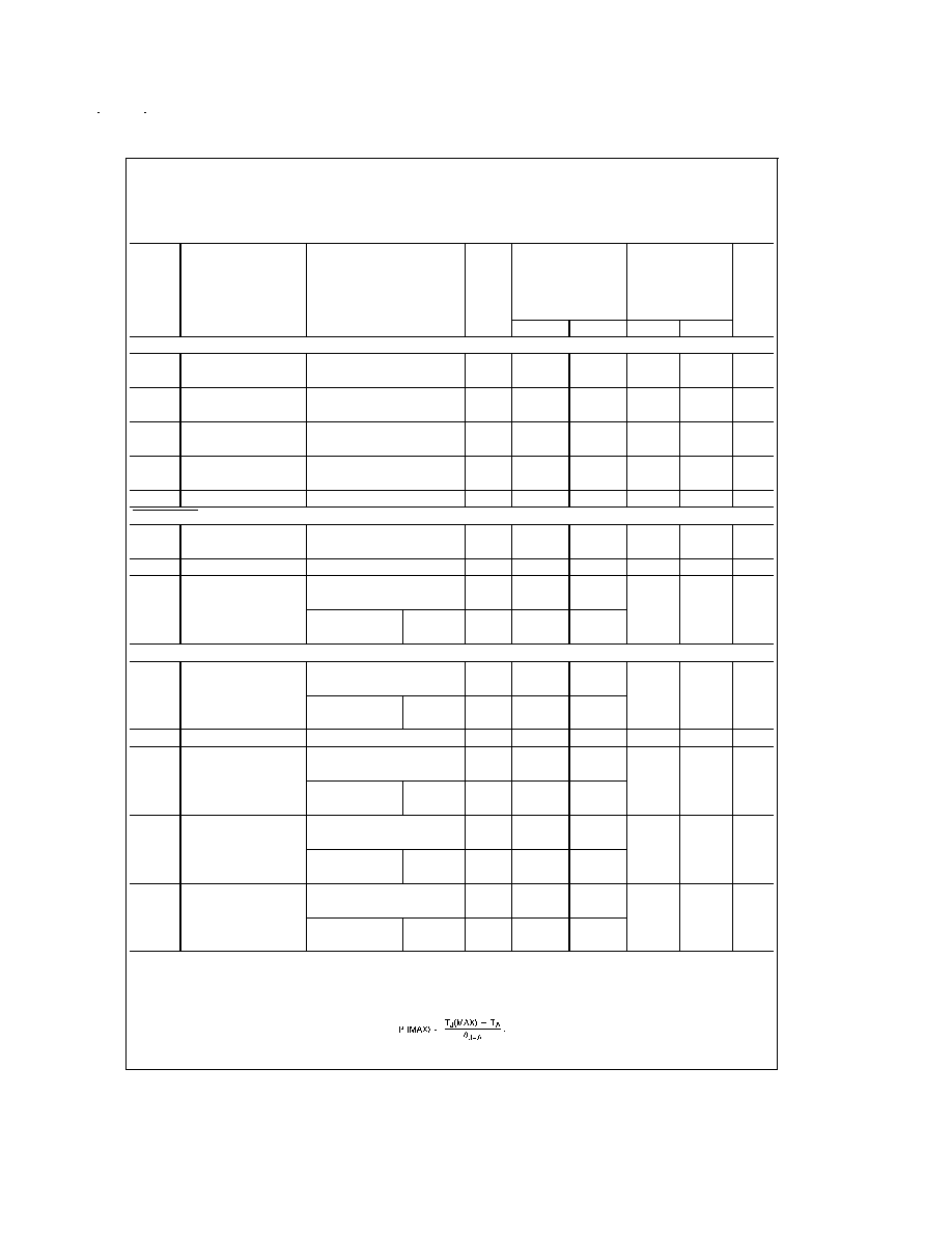
Electrical Characteristics
Limits in standard typeface are for T
J
= 25∞C, bold typeface applies over the full
operating temperature range. Limits are guaranteed by production testing or correlation techniques using standard Statistical
Quality Control (SQC) methods. Unless otherwise specified: V
IN
= V
O
(NOM) + 1V, I
L
= 1 mA, C
L
= 2.2 µF for 5V parts and
4.7µF for 3.3V parts. Feedback pin is tied to V Tap pin, Output pin is tied to Output Sense pin.
3.3V Versions
Symbol
Parameter
Conditions
Typical
LP2952AI-3.3, LP2953AI-3.3
LP2952I-3.3, LP2953I-3.3
Units
Min
Max
Min
Max
V
O
Output Voltage
3.3
3.284
3.317
3.267
3.333
V
3.260
3.340
3.234
3.366
1 mA
I
L
250 mA
3.3
3.254
3.346
3.221
3.379
5V Versions
Symbol
Parameter
Conditions
Typical
LP2952AI, LP2953AI,
LP2952I, LP2953I
Units
LP2953AM (Note 17)
Min
Max
Min
Max
V
O
Output Voltage
5.0
4.975
5.025
4.950
5.050
V
4.940
5.060
4.900
5.100
1 mA
I
L
250 mA
5.0
4.930
5.070
4.880
5.120
All Voltage Options
Electrical Characteristics
Limits in standard typeface are for T
J
= 25∞C, bold typeface applies over the full operating temperature range. Limits are guar-
anteed by production testing or correlation techniques using standard Statistical Quality Control (SQC) methods. Unless other-
wise specified: V
IN
= V
O
(NOM) + 1V, I
L
= 1 mA, C
L
= 2.2 µF for 5V parts and 4.7µF for 3.3V parts. Feedback pin is tied to V
Tap pin, Output pin is tied to Output Sense pin.
Symbol
Parameter
Conditions
Typical
LP2952AI,
LP2953AI,
LP2952AI-3.3,
LP2953AI-3.3,
LP2953AM
(Notes 16, 17)
LP2952I, LP2953I,
LP2952I-3.3,
LP2953I-3.3
Units
Min
Max
Min
Max
REGULATOR
Output Voltage Temp.
Coefficient
(Note 5)
20
100
150
ppm/∞C
Output Voltage Line
Regulation
V
IN
= V
O
(NOM) + 1V to 30V
0.03
0.1
0.2
%
0.2
0.4
Output Voltage Load
Regulation (Note 6)
I
L
= 1 mA to 250 mA
0.04
0.16
0.20
%
I
L
= 0.1 mA to 1 mA
0.20
0.30
www.national.com
3
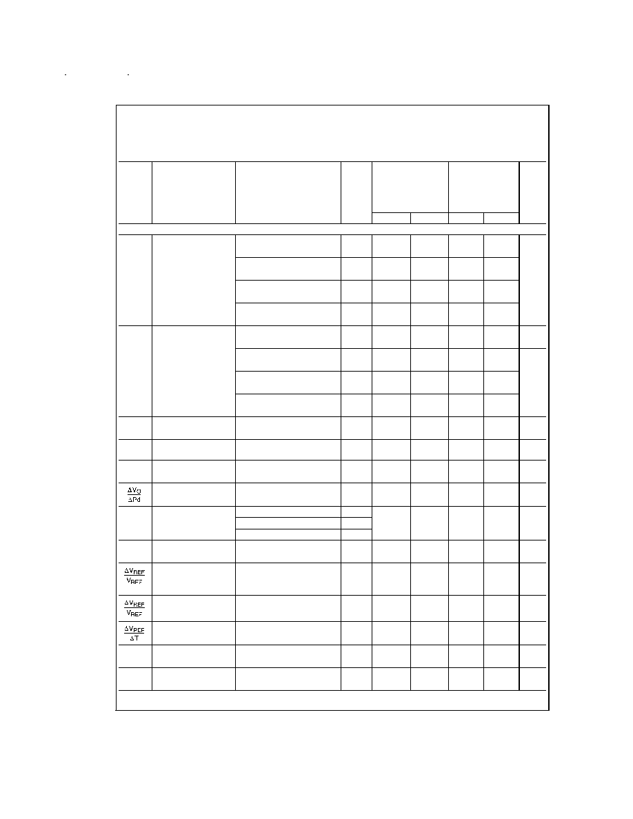
Electrical Characteristics
(Continued)
Limits in standard typeface are for T
J
= 25∞C, bold typeface applies over the full operating temperature range. Limits are guar-
anteed by production testing or correlation techniques using standard Statistical Quality Control (SQC) methods. Unless other-
wise specified: V
IN
= V
O
(NOM) + 1V, I
L
= 1 mA, C
L
= 2.2 µF for 5V parts and 4.7µF for 3.3V parts. Feedback pin is tied to V
Tap pin, Output pin is tied to Output Sense pin.
Symbol
Parameter
Conditions
Typical
LP2952AI,
LP2953AI,
LP2952AI-3.3,
LP2953AI-3.3,
LP2953AM
(Notes 16, 17)
LP2952I, LP2953I,
LP2952I-3.3,
LP2953I-3.3
Units
Min
Max
Min
Max
REGULATOR
V
IN
≠V
O
Dropout Voltage
(Note 7)
I
L
= 1 mA
60
100
100
mV
150
150
I
L
= 50 mA
240
300
300
420
420
I
L
= 100 mA
310
400
400
520
520
I
L
= 250 mA
470
600
600
800
800
I
GND
Ground Pin Current
(Note 8)
I
L
= 1 mA
130
170
170
µA
200
200
I
L
= 50 mA
1.1
2
2
mA
2.5
2.5
I
L
= 100 mA
4.5
6
6
8
8
I
L
= 250 mA
21
28
28
33
33
I
GND
Ground Pin Current at
Dropout
V
IN
= V
O
(NOM) -0.5V
165
210
210
µA
I
L
= 100 µA
240
240
I
GND
Ground Pin Current at
Shutdown (Note 8)
V
SHUTDOWN
1.1V
105
140
140
µA
I
LIMIT
Current Limit
V
OUT
= 0
380
500
500
mA
530
530
Thermal Regulation
(Note 10)
0.05
0.2
0.2
%/W
e
n
Output Noise Voltage
(10 Hz to 100 kHz)
I
L
= 100 mA
C
L
= 4.7 µF
400
µV
RMS
C
L
= 33 µF
260
C
L
= 33 µF (Note 11)
80
V
REF
Reference Voltage
(Note 12)
1.230
1.215
1.245
1.205
1.255
V
1.205
1.255
1.190
1.270
Reference Voltage
Line Regulation
V
IN
= 2.5V to V
O
(NOM) + 1V
0.03
0.1
0.2
%
V
IN
= V
O
(NOM) + 1V to 30V
(Note 13)
0.2
0.4
Reference Voltage
Load Regulation
I
REF
= 0 to 200 µA
0.25
0.4
0.8
%
0.6
1.0
Reference Voltage
Temp. Coefficient
(Note 5)
20
ppm/∞C
I
B
(FB)
Feedback Pin Bias
Current
20
40
40
nA
60
60
I
O
(SINK)
Output "OFF" Pulldown
Current
(Note 9)
30
30
mA
20
20
www.national.com
4
Electrical Characteristics
(Continued)
Limits in standard typeface are for T
J
= 25∞C, bold typeface applies over the full operating temperature range. Limits are guar-
anteed by production testing or correlation techniques using standard Statistical Quality Control (SQC) methods. Unless other-
wise specified: V
IN
= V
O
(NOM) + 1V, I
L
= 1 mA, C
L
= 2.2 µF for 5V parts and 4.7µF for 3.3V parts. Feedback pin is tied to V
Tap pin, Output pin is tied to Output Sense pin.
Symbol
Parameter
Conditions
Typical
LP2952AI,
LP2953AI,
LP2952AI-3.3,
LP2953AI-3.3,
LP2953AM
(Notes 16, 17)
LP2952I, LP2953I,
LP2952I-3.3,
LP2953I-3.3
Units
Min
Max
Min
Max
DROPOUT DETECTION COMPARATOR
I
OH
Output "HIGH"
Leakage
V
OH
= 30V
0.01
1
1
µA
2
2
V
OL
Output "LOW" Voltage
V
IN
= V
O
(NOM) - 0.5V
I
O
(COMP) = 400 µA
150
250
250
mV
400
400
V
THR
(MAX)
Upper Threshold
Voltage
(Note 14)
-60
-80
-35
-80
-35
mV
-95
-25
-95
-25
V
THR
(MIN)
Lower Threshold
Voltage
(Note 14)
-85
-110
-55
-110
-55
mV
-160
-40
-160
-40
HYST
Hysteresis
(Note 14)
15
mV
SHUTDOWN INPUT (Note 15)
V
OS
Input Offset
(Referred to V
REF
)
±
3
-7.5
7.5
-7.5
7.5
mV
Voltage
-10
10
-10
10
HYST
Hysteresis
6
mV
I
B
Input Bias
V
IN
(S/D) = 0V to 5V
10
-30
30
-30
-50
-30
50
nA
Current
-50
50
LP2953AM
10
-30
30
-75
75
AUXILIARY COMPARATOR (LP2953 Only)
V
OS
Input Offset Voltage
(Referred to V
REF
)
±
3
-7.5
7.5
-7.5
-10
7.5
10
mV
-10
10
LP2953AM
±
3
-7.5
7.5
-12
12
HYST
Hysteresis
6
mV
I
B
Input Bias Current
V
IN
(COMP) = 0V to 5V
10
-30
30
-30
-50
30
50
nA
-50
50
LP2953AM
10
-30
30
-75
75
I
OH
Output "HIGH"
Leakage
V
OH
= 30V
0.01
1
1
2
µA
V
IN
(COMP) = 1.3V
2
LP2953AM
0.01
1
2.2
V
OL
Output "LOW" Voltage
V
IN
(COMP) = 1.1V
150
250
250
400
mV
I
O
(COMP) = 400 µA
400
LP2953AM
150
250
420
Note 1: Absolute maximum ratings indicate limits beyond which damage to the component may occur. Electrical specifications do not apply when operating the de-
vice outside of its rated operating conditions.
Note 2: The maximum allowable power dissipation is a function of the maximum junction temperature, T
J
(MAX), the junction-to-ambient thermal resistance,
J≠A
,
and the ambient temperature, T
A
. The maximum allowable power dissipation at any ambient temperature is calculated using the equation for P(MAX),
.
www.national.com
5