 | –≠–ª–µ–∫—Ç—Ä–æ–Ω–Ω—ã–π –∫–æ–º–ø–æ–Ω–µ–Ω—Ç: LP2954ISX | –°–∫–∞—á–∞—Ç—å:  PDF PDF  ZIP ZIP |
LP2954/LP2954A
5V and Adjustable Micropower Low-Dropout Voltage
Regulators
General Description
The LP2954 is a 5V micropower voltage regulator with very
low quiescent current (90 µA typical at 1 mA load) and very
low dropout voltage (typically 60 mV at light loads and
470 mV at 250 mA load current).
The quiescent current increases only slightly at dropout
(120 µA typical), which prolongs battery life.
The LP2954 with a fixed 5V output is available in the
three-lead TO-220 and TO-263 packages. The adjustable
LP2954 is provided in an 8-lead surface mount, small outline
package. The adjustable version also provides a resistor net-
work which can be pin strapped to set the output to 5V.
Reverse battery protection is provided.
The tight line and load regulation (0.04% typical), as well as
very low output temperature coefficient make the LP2954
well suited for use as a low-power voltage reference.
Output accuracy is guaranteed at both room temperature
and over the entire operating temperature range.
Features
n
5V output within 1.2% over temperature (A grade)
n
Adjustable 1.23 to 29V output voltage available
(LP2954IM and LP2954AIM)
n
Guaranteed 250 mA output current
n
Extremely low quiescent current
n
Low dropout voltage
n
Reverse battery protection
n
Extremely tight line and load regulation
n
Very low temperature coefficient
n
Current and thermal limiting
n
Pin compatible with LM2940 and LM340 (5V version
only)
n
Adjustable version adds error flag to warn of output drop
and a logic-controlled shutdown
Applications
n
High-efficiency linear regulator
n
Low dropout battery-powered regulator
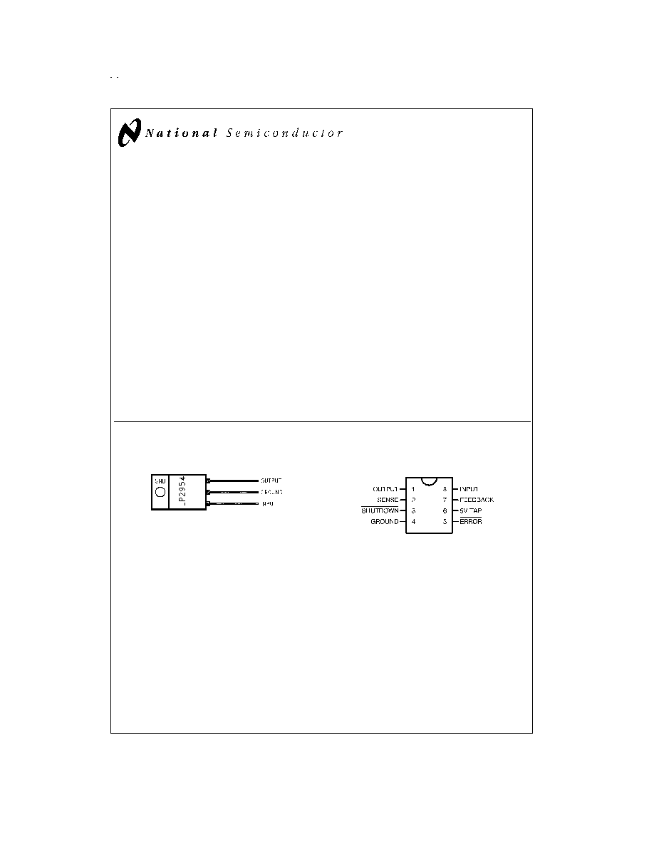
Package Outline and Ordering Information
TO-220 3≠Lead Plastic Package
DS011128-2
Front View
Order Number LP2954AIT or LP2954IT
See NS Package T03B
SO-8 Small Outline Surface Mount
DS011128-33
Top View
Order Number LP2954AIM or LP2954IM
See NS Package M08A
June 1999
LP2954/LP2954A
5V
and
Adjustable
Micropower
Low-Dropout
V
oltage
Regulators
© 1999 National Semiconductor Corporation
DS011128
www.national.com
Package Outline and Ordering Information
(Continued)
Ordering Information
Order Number
Temp. Range
Package
NS Package
(T
J
) ∞C
(JEDEC)
Number
LP2954AIT
-40 to +125
TO-220
TO3B
LP2954IT
LP2954AIS
-40 to +125
TO-263
TS3B
LP2954IS
LP2954AIM
-40 to +125
SO-8
M08A
LP2954IM
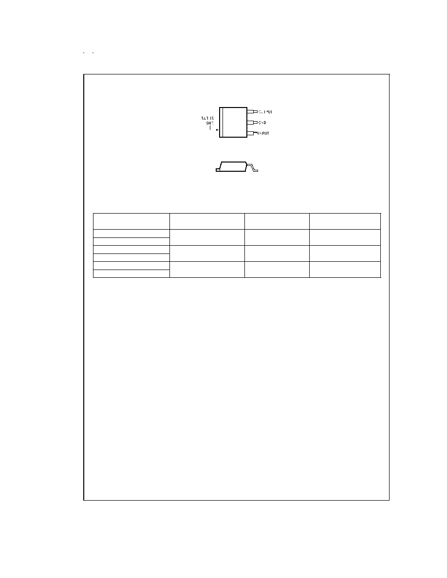
TO-263 3-Lead Plastic Surface-Mount Package
DS011128-9
Top View
DS011128-10
Side View
Order Number LP2954AIS or LP2954IS
See NS Package TS3B
www.national.com
2

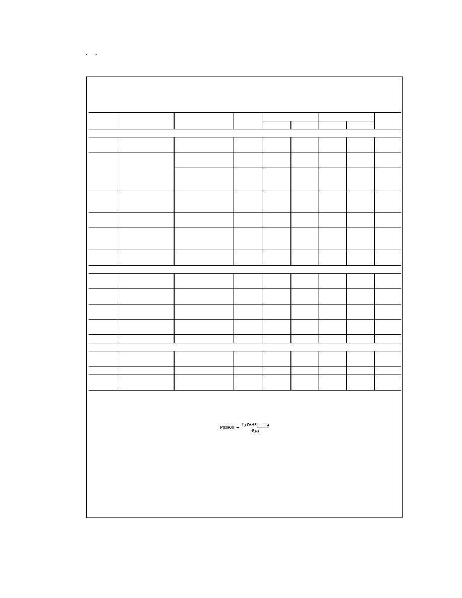
Absolute Maximum Ratings
(Note 1)
If Military/Aerospace specified devices are required,
please contact the National Semiconductor Sales Office/
Distributors for availability and specifications.
Operating Junction Temperature
Range
LP2954AI/LP2954I
-40∞C to +125∞C
Storage Temperature Range
-65∞C to +150∞C
Lead Temperature
(Soldering, 5 seconds)
260∞C
Power Dissipation (Note 2)
Internally Limited
Input Supply Voltage
-20V to +30V
ESD Rating
2 kV
Electrical Characteristics
Limits in standard typeface are for T
J
= 25∞C, bold typeface applies over the -40∞C to +125∞C temperature range. Limits
are guaranteed by production testing or correlation techniques using standard Statistical Quality Control (SQC) methods. Un-
less otherwise noted: V
IN
= 6V, I
L
= 1 mA, C
L
= 2.2 µF.
Symbol
Parameter
Conditions
Typical
2954AI
2954I
Units
Min
Max
Min
Max
V
O
Output Voltage
5.0
4.975
5.025
4.950
5.050
V
4.940
5.060
4.900
5.100
1 mA
I
L
250 mA
5.0
4.930
5.070
4.880
5.120
Output Voltage
(Note 3)
20
100
150
ppm/∞C
Temp. Coefficient
Line Regulation
V
IN
= 6V to 30V
0.03
0.10
0.20
%
0.20
0.40
Load Regulation
I
L
= 1 to 250 mA
0.16
0.20
I
L
= 0.1 to 1 mA
0.04
0.20
0.30
%
(Note 4)
V
IN
≠V
O
Dropout Voltage
I
L
= 1 mA
60
100
100
mV
(Note 5)
150
150
I
L
= 50 mA
240
300
300
420
420
I
L
= 100 mA
310
400
400
520
520
I
L
= 250 mA
470
600
600
800
800
I
GND
Ground Pin Current
I
L
= 1 mA
90
150
150
µA
(Note 6)
180
180
I
L
= 50 mA
1.1
2
2
mA
2.5
2.5
I
L
= 100 mA
4.5
6
6
8
8
I
L
= 250 mA
21
28
28
33
33
I
GND
Ground Pin
V
IN
= 4.5V
170
170
Current at Dropout
120
210
210
µA
(Note 6)
I
LIMIT
Current Limit
V
OUT
= 0V
380
500
500
mA
530
530
Thermal Regulation
(Note 7)
0.05
0.2
0.2
%/W
e
n
Output Noise
C
L
= 2.2 µF
400
µV RMS
Voltage
(10 Hz to 100 kHz)
C
L
= 33 µF
260
I
L
= 100 mA
C
L
=33µF(Note 9)
80
www.national.com
3
Electrical Characteristics
(Continued)
Limits in standard typeface are for T
J
= 25∞C, bold typeface applies over the -40∞C to +125∞C temperature range. Limits
are guaranteed by production testing or correlation techniques using standard Statistical Quality Control (SQC) methods. Un-
less otherwise noted: V
IN
= 6V, I
L
= 1 mA, C
L
= 2.2 µF.
Symbol
Parameter
Conditions
Typical
2954AI
2954I
Units
Min
Max
Min
Max
Additional Specifications for the Adjustable Device (LP2954AIM and LP2954IM)
V
REF
Reference Voltage
(Note 10)
1.230
1.215
1.205
1.245
1.255
1.205
1.190
1.255
1.270
V
V
REF
/
V
REF
Reference Voltage
Line Regulation
V
IN
=2.5V to
VO(NOM)+1V
0.03
0.1
0.2
V
IN
=2.5V to
VO(NOM)+1V to 30V
(Note 11)
0.2
0.4
V
REF
/
T
Reference Voltage
Temperature
Coefficient
(Note 3)
20
ppm/∞C
I
B
(FB)
Feedback Pin Bias
Current
20
40
60
40
60
nA
I
GND
Ground Pin Current
at Shutdown (Note
6)
V
SHUTDOWN
1.1V
105
140
140
µA
I
O
(SINK)
Output
OFF
Pulldown Current
(Note 12)
30
20
30
20
mA
Dropout Detection Comparator
I
OH
Output
HIGH
Leakage Current
V
OH
=30V
0.01
1
2
1
2
µA
V
OL
Output
LOW
Voltage
V
IN
=V
O
(NOM)-0.5V
I
O
(COMP)=400µA
150
250
400
250
400
mV
V
THR
(MAX)
Upper Threshold
Voltage
(Note 13)
-60
-80
-95
-35
-25
-80
-95
-35
-25
mV
V
THR
(MIN)
Lower Threshold
Voltage
(Note 13)
-85
-110
-160
-55
-40
-110
-160
-55
-40
mV
HYST
Hysteresis
(Note 13)
15
mV
Shutdown Input
V
OS
Input Offset Voltage
(Referred to V
REF
)
±
3
-7.5
-10
7.5
10
-7.5
-10
7.5
10
mV
HYST
Hysteresis
6
mV
I
B
Input Bias Current
V
IN
(S/D)=0V to 5V
10
-30
-50
30
50
-30
-50
30
50
nA
Note 1: Absolute maximum ratings indicate limits beyond which damage to the component may occur. Electrical specifications do not apply when operating the de-
vice outside of its rated operating conditions.
Note 2: The maximum allowable power dissipation is a function of the maximum junction temperature, T
J
(MAX), the junction-to-ambient thermal resistance,
J-A
,
and the ambient temperature, T
A
. The maximum allowable power dissipation at any ambient temperature is calculated using:
.
Exceeding the maximum allowable power dissipation will result in excessive die temperature, and the regulator will go into thermal shutdown. The junction-to-ambient
thermal resistance of the TO-220 (without heatsink) is 60∞C/W, 73∞C/W for the TO-263, and 160∞C/W for the SO-8. If the TO-263 package is used, the thermal re-
sistance can be reduced by increasing the P.C. board copper area thermally connected to the package: Using 0.5 square inches of copper area,
JA
is 50∞C/W; with
1 square inch of copper area,
JA
is 37∞C/W; and with 1.6 or more square inches of copper area,
JA
is 32∞C/W. The junction-to-case thermal resistance is 3∞C/W.
If an external heatsink is used, the effective junction-to-ambient thermal resistance is the sum of the junction-to-case resistance (3∞C/W), the specified thermal re-
sistance of the heatsink selected, and the thermal resistance of the interface between the heatsink and the LP2954. Some typical values are listed for interface ma-
terials used with TO-220:
www.national.com
4

Electrical Characteristics
(Continued)
TABLE 1. Typical Values of Case-to-Heatsink
Thermal Resistance (∞C/W) (Data from AAVID Eng.)
Silicone grease
1.0
Dry interface
1.3
Mica with grease
1.4
TABLE 2. Typical Values of Case-to-Heatsink
Thermal Resistance (∞C/W) (Data from Thermalloy)
Thermasil III
1.3
Thermasil II
1.5
Thermalfilm (0.002) with grease
2.2
Note 3: Output voltage temperature coefficient is defined as the worst case voltage change divided by the total temperature range.
Note 4: Regulation is measured at constant junction temperature using low duty cycle pulse testing. Parts are tested separately for load regulation in the load
ranges 0.1 mA≠1 mA and 1 mA≠250 mA. Changes in output voltage due to heating effects are covered by the thermal regulation specification.
Note 5: Dropout voltage is defined as the input to output differential at which the output voltage drops 100 mV below the value measured with a 1V differential.
Note 6: Ground pin current is the regulator quiescent current. The total current drawn from the source is the sum of the load current plus the ground pin current.
Note 7: Thermal regulation is defined as the change in output voltage at a time T after a change in power dissipation is applied, excluding load or line regulation
effects. Specifications are for 200 mA load pulse at V
IN
= 20V (3W pulse) for T = 10 ms.
Note 8: When used in dual-supply systems where the regulator load is returned to a negative supply, the output voltage must be diode-clamped to ground.
Note 9: Connect a 0.1µF capacitor from the output to the feedback pin.
Note 10: V
REF
V
OUT
(V
IN
-1V), 2.3V
V
IN
30V, 100µA
I
L
250mA.
Note 11: Two seperate tests are performed, one covering V
IN
=2.5V to V
O
(NOM)+1V and the other test for V
IN
=2.5V to V
O
(NOM)+1V to 30V.
Note 12: V
SHUTDOWN
1.1V, VOUT=V
O
(NOM).
Note 13: Comparator thresholds are expressed in terms of a voltage differential at the Feedback terminal below the nominal reference voltage measured at
V
IN
=V
O
(NOM)+1V. To express these thresholds in terms of output voltage change, multiply by the Error amplifier gain, which is V
OUT
/V
REF
=(R1+R2)/R2.
Note 14: Human body model, 200pF discharged through 1.5k
.
Typical Performance Characteristics
Quiescent Current
DS011128-12
Quiescent Current
DS011128-13
Ground Pin Current vs Load
DS011128-14
Ground Pin Current
DS011128-15
Ground Pin Current
DS011128-16
Output Noise Voltage
DS011128-17
www.national.com
5