 | ÐлекÑÑоннÑй компоненÑ: LP2957AI | СкаÑаÑÑ:  PDF PDF  ZIP ZIP |
LP2957/LP2957A 5V Low-Dropout Regulator for µP Applications
LP2957/LP2957A
5V Low-Dropout Regulator for µP Applications
General Description
The LP2957 is a 5V micropower voltage regulator with elec-
tronic shutdown, error flag, very low quiescent current
(150 µA typical at 1 mA load), and very low dropout voltage
(470 mV typical at 250 mA load current).
Output can be wired for snap-on/snap-off operation to elimi-
nate transition voltage states where µP operation may be un-
predictable.
Output crowbar (50 mA typical pull-down current) will bring
down the output quickly when the regulator snaps off or
when the shutdown function is activated.
The part has tight line and load regulation (0.04% typical)
and low output temperature coefficient (20 ppm/°C typical).
The accuracy of the 5V output is guaranteed at room tem-
perature and over the full operating temperature range.
The LP2957 is available in the five-lead TO-220 and TO-263
packages.
Features
n
5V output within 1.4% over temperature (A grade)
n
Easily programmed for snap-on/snap-off output
n
Guaranteed 250 mA output current
n
Extremely low quiescent current
n
Low Input-Output voltage required for regulation
n
Reverse battery protection
n
Extremely tight line and load regulation
n
Very low temperature coefficient
n
Current and thermal limiting
n
Error flag signals when output is out of regulation
Applications
n
High-efficiency linear regulator
n
Battery-powered regulator
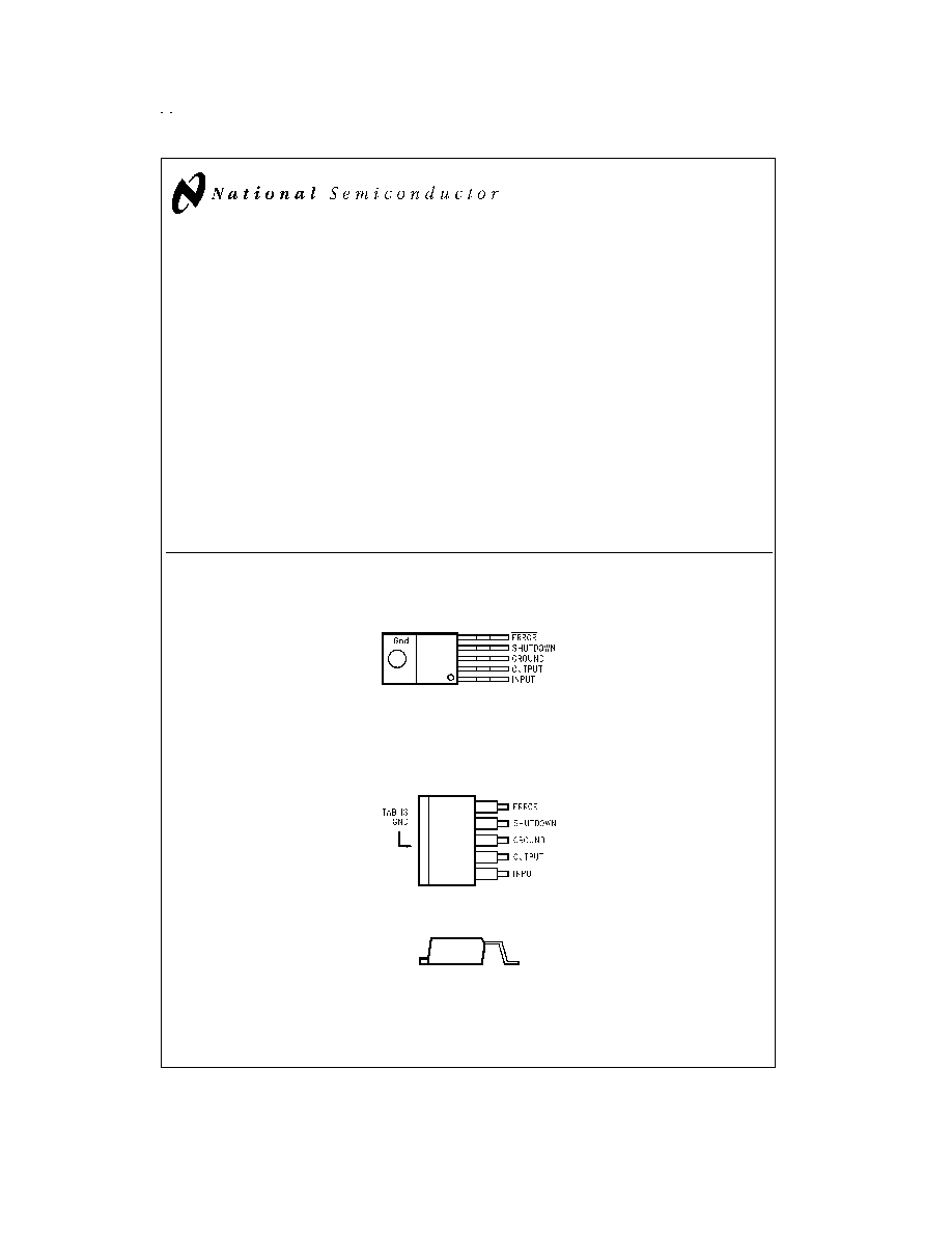
Package Outline
Bent, Staggered Leads
5-Lead TO-220 (T)
DS011340-16
Top View
Order Number LP2957AIT or LP2957IT
See NS Package Number T05D
Plastic Surface Mount Package
5-Lead TO-263 (S)
DS011340-17
Top View
DS011340-18
Side View
Order Number LP2957AIS or LP2957IS
See NS Package Number TS5B
June 1998
LP2957/LP2957A
5V
Low-Dropout
Regulator
for
µP
Applications
© 1999 National Semiconductor Corporation
DS011340
www.national.com
Absolute Maximum Ratings
(Note 1)
If Military/Aerospace specified devices are required,
please contact the National Semiconductor Sales Office/
Distributors for availability and specifications.
Operating Junction
Temperature Range
-40°C to +125°C
Storage Temperature Range
-65°C to +150°C
Lead Temperature
(Soldering, 5 Seconds)
260°C
Power Dissipation (Note 2)
Internally Limited
Input Supply Voltage
-20V to +30V
Shutdown Input
-0.3V to +30V
ESD Rating
2 kV
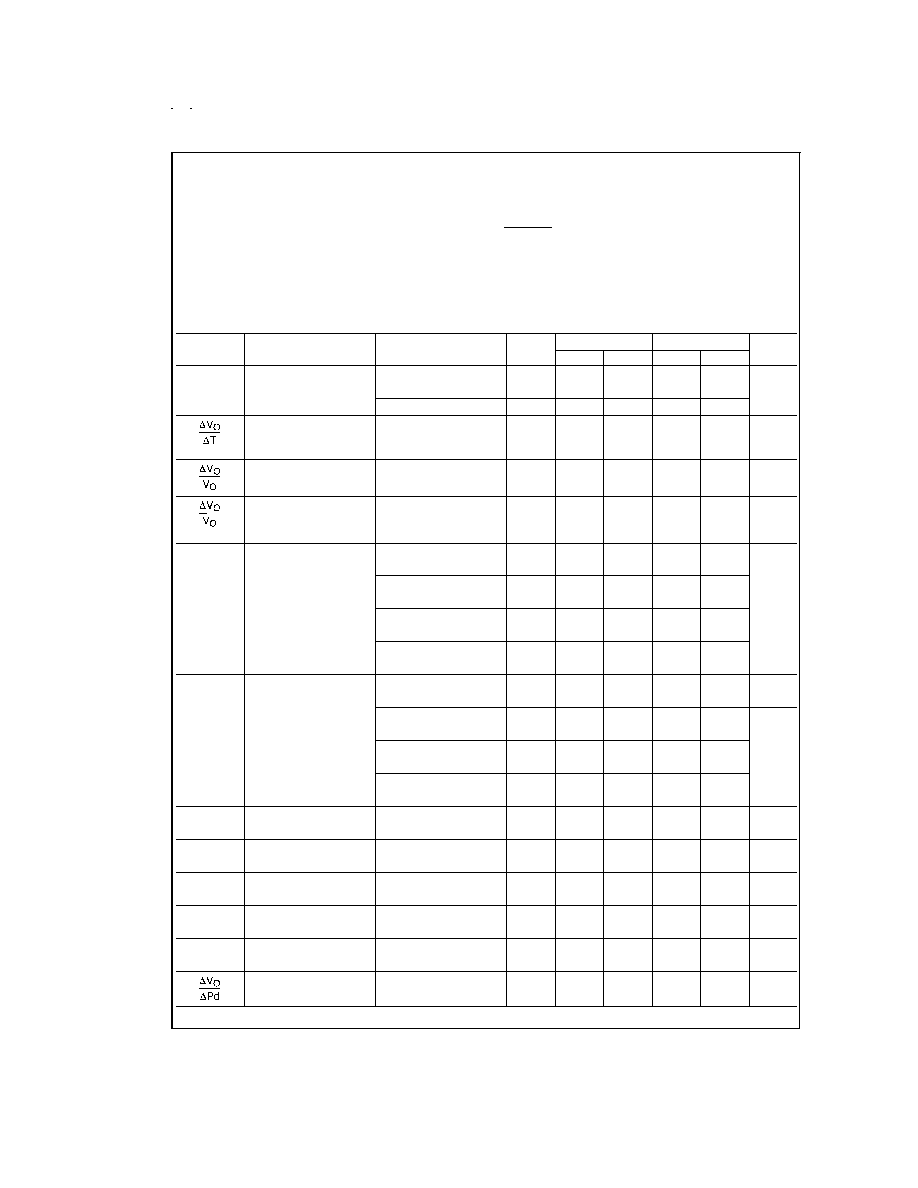
Electrical Characteristics
Limits in standard typeface are for T
J
= 25°C, and limits in boldface type apply over the full operating temperature range. Un-
less otherwise specified: V
IN
= 6V, I
L
= 1 mA, C
L
= 2.2 µF, V
SD
= 3V.
Symbol
Parameter
Conditions
Typical
LP2957AI
LP2957I
Units
Min
Max
Min
Max
V
O
Output Voltage
5.0
4.975
5.025
4.950
5.050
V
(Note 9)
4.940
5.060
4.900
5.100
1 mA
I
L
250 mA
5.0
4.930
5.070
4.880
5.120
Output Voltage
Temperature
Coefficient
(Note 3)
20
100
150
ppm/°C
Line Regulation
V
IN
= 6V to 30V
0.03
0.10
0.20
%
0.20
0.40
Load Regulation
I
L
= 1 mA to 250 mA
0.04
0.16
0.20
%
I
L
= 0.1 mA to 1 mA
(Note 4)
0.20
0.30
V
IN
V
O
Dropout Voltage
I
L
= 1 mA
60
100
100
mV
(Note 5)
150
150
I
L
= 50 mA
240
300
300
420
420
I
L
= 100 mA
310
400
400
520
520
I
L
= 250 mA
470
600
600
800
800
I
GND
Ground Pin Current
I
L
= 1 mA
150
200
200
µA
(Note 6)
230
230
I
L
= 50 mA
1.1
2
2
mA
2.5
2.5
I
L
= 100 mA
3
6
6
8
8
I
L
= 250 mA
16
28
28
33
33
I
GND
Ground Pin Current
I
L
= 0
130
180
180
µA
in Shutdown (Note 6)
V
SD
= 0.4V
200
200
I
GND
Ground Pin Current
V
IN
= 4.5V
180
230
230
µA
at Dropout (Note 6)
I
L
= 0.1 mA
250
250
I
O
Off-State Output
V
IN
= 5.3V
50
30
30
mA
(Sink)
Pulldown Current
V
O
= 5V, V
SD
= 0.4V
20
20
I
O
Output Leakage
I
(SD IN)
1 µA
3
10
10
µA
(Off)
in Shutdown
V
IN
= 30V, V
OUT
= 0V
20
20
I
LIMIT
Current Limit
R
L
= 1
400
500
500
mA
530
530
Thermal Regulation
(Note 7)
0.05
0.2
0.2
%/W
www.national.com
2
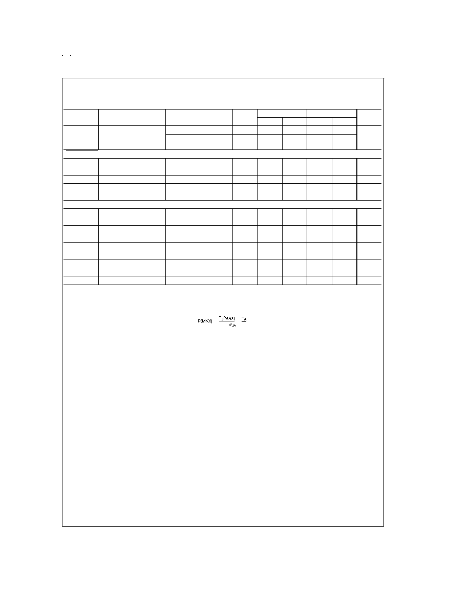
Electrical Characteristics
(Continued)
Limits in standard typeface are for T
J
= 25°C, and limits in boldface type apply over the full operating temperature range. Un-
less otherwise specified: V
IN
= 6V, I
L
= 1 mA, C
L
= 2.2 µF, V
SD
= 3V.
Symbol
Parameter
Conditions
Typical
LP2957AI
LP2957I
Units
Min
Max
Min
Max
e
n
Output Noise Voltage
C
L
= 2.2 µF
500
µV
RMS
(10 Hz to 100 kHz)
I
L
= 100 mA
C
L
= 33 µF
320
SHUTDOWN INPUT
V
SD
(ON)
Output Turn-On
1.155
1.305
1.155
1.305
V
Threshold Voltage
1.140
1.320
1.140
1.320
HYST
Hysteresis
6
mV
I
B
Input Bias
V
IN(SD)
= 0V to 5V
10
-30
30
-30
30
nA
Current
-50
50
-50
50
DROPOUT DETECTION COMPARATOR
I
OH
Output "HIGH"
V
OH
= 30V
0.01
1
1
µA
Leakage
2
2
V
OL
Output "LOW"
V
IN
= 4V
150
250
250
mV
Voltage
I
O
(COMP) = 400 µA
400
400
V
THR
Upper Threshold
(Note 8)
-240
-320
-150
-320
-150
mV
(Max)
Voltage
-380
-100
-380
-100
V
THR
Lower Threshold
(Note 8)
-350
-450
-230
-450
-230
mV
(Min)
Voltage
-640
-160
-640
-160
HYST
Hysteresis
(Note 8)
60
mV
Note 1: Absolute maximum ratings indicate limits beyond which damage to the component may occur. Electrical specifications do not apply when operating the de-
vice outside of its rated operating conditions.
Note 2: The maximum allowable power dissipation is a function of the maximum junction temperature, T
J
(MAX), the junction-to-ambient thermal resistance,
JA
,
and the ambient temperature, T
A
. The maximum allowable power dissipation at any ambient temperature is calculated using:
Exceeding the maximum allowable power dissipation will result in excessive die temperature, and the regulator will go into thermal shutdown. The junction-to-ambient
thermal resistance of the TO-220 (without heatsink) is 60°C/W and 73°C/W for the TO-263. If the TO-263 package is used, the thermal resistance can be reduced
by increasing the P.C. board copper area thermally connected to the package: Using 0.5 Square inches of copper area,
JA
is 50°C/W, with 1 square inch of copper
area,
JA
is 37°C/W; and with 1.6 or more square inches of copper area,
JA
is 32°C/W. The junction-to-case thermal resistance is 3°C/W. If an external heatsink is
used, the effective junction-to-ambient thermal resistance is the sum of the junction-to-case resistance (3°C/W), the specified thermal resistance of the heatsink se-
lected, and the thermal resistance of the interface between the heatsink and the LP2957 (see Application Hints).
Note 3: Output voltage temperature coefficient is defined as the worst case voltage change divided by the total temperature range.
Note 4: Regulation is measured at constant junction temperature using low duty cycle pulse testing. Parts are tested separately for load regulation in the load ranges
0.1 mA1 mA and 1 mA250 mA. Changes in output voltage due to heating effects are covered by the thermal regulation specification.
Note 5: Dropout voltage is defined as the input to output voltage differential at which the output voltage drops 100 mV below the value measured with a 1V input
to output differential.
Note 6: Ground pin current is the regulator quiescent current. The total current drawn from the source is the sum of the load current plus the ground pin current.
Note 7: Thermal regulation is defined as the change in output voltage at a time T after a change in power dissipation is applied, excluding load or line regulation ef-
fects. Specifications are for a 200 mA load pulse at V
IN
= 20V (3W pulse) for T = 10 ms.
Note 8: Voltages are referenced to the nominal regulated output voltage.
Note 9: When used in dual-supply systems where the regulator load is returned to a negative supply, the output voltage must be diode-clamped to ground.
www.national.com
3
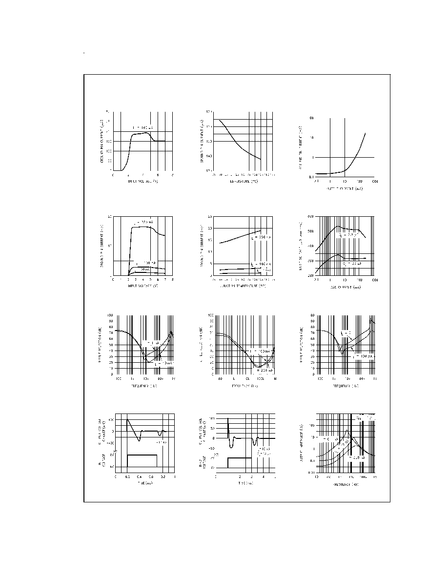
Typical Performance Characteristics
Unless otherwise specified: V
IN
= 6V, I
L
= 1 mA, C
L
= 2.2 µF, V
SD
= 3V, T
A
= 25°C
Ground Pin Current
DS011340-19
Ground Pin Current
DS011340-20
Ground Pin Current
vs Load
DS011340-21
Ground Pin Current
DS011340-22
Ground Pin Current
DS011340-23
Output Noise Voltage
DS011340-24
Ripple Rejection
DS011340-25
Ripple Rejection
DS011340-26
Ripple Rejection
DS011340-27
Line Transient Response
DS011340-28
Line Transient Response
DS011340-29
Output Impedance
DS011340-30
www.national.com
4
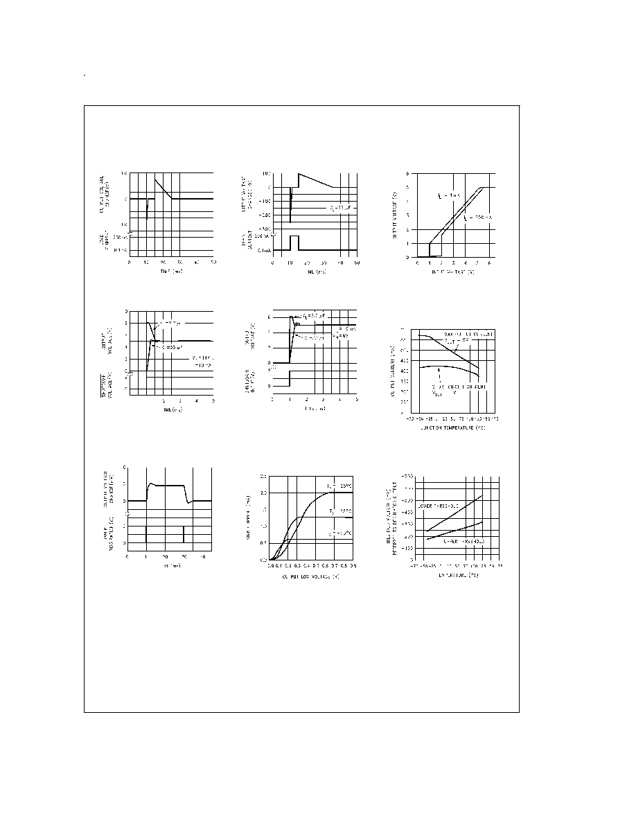
Typical Performance Characteristics
Unless otherwise specified: V
IN
= 6V, I
L
= 1 mA, C
L
= 2.2 µF,
V
SD
= 3V, T
A
= 25°C (Continued)
Load Transient
Response
DS011340-31
Load Transient
Response
DS011340-32
Dropout
Characteristics
DS011340-33
Enable Transient
DS011340-34
Enable Transient
DS011340-35
Short-Circuit Output
Current and Maximum
Output Current
DS011340-36
Thermal Regulation
DS011340-37
Error Output
Sink Current
DS011340-38
Dropout Detection
Threshold Voltages
DS011340-39
www.national.com
5