LP2978
Micropower SOT, 50 mA Low-Noise Ultra Low-Dropout
Regulator
Designed for Use with Very Low ESR Output Capacitors
General Description
The LP2978 is a 50 mA, fixed-output voltage regulator de-
signed to provide ultra low-dropout and low noise in battery
powered applications.
Using an optimized VIP
TM
(Vertically Integrated PNP) pro-
cess, the LP2978 delivers unequalled performance in all
specifications critical to battery-powered designs:
Dropout Voltage: Typically 120 mV
@
50 mA load, and 7 mV
@
1 mA load.
Ground Pin Current: Typically 350 µA
@
50 mA load, and
75 µA
@
1 mA load.
Enhanced Stability: The LP2978 is stable with output ca-
pacitor ESR as low as 5 m
, which allows the use of ceramic
capacitors on the output.
Sleep Mode: Less than 1 µA quiescent current when
ON/OFF pin is pulled low.
Smallest Possible Size: SOT-23 package uses absolute
minimum board space.
Precision Output: 1% tolerance output voltages available
(A grade).
Low Noise: By adding a 10 nF bypass capacitor, output
noise can be reduced to 30 µV (typical).
Features
n
Ultra low dropout voltage
n
Smallest possible size (SOT-23 Package)
n
Requires minimum external components
n
Stable with low-ESR output capacitor
n
<
1 µA quiescent current when shut down
n
Low ground pin current at all loads
n
Output voltage accuracy 1% (A Grade)
n
High peak current capability
n
Wide supply voltage range (16V max)
n
Low Z
OUT
: 0.3
typical (10 Hz to 1 MHz)
n
Overtemperature/overcurrent protection
n
-40∞C to +125∞C junction temperature range
n
Custom voltages available
Applications
n
Cellular Phone
n
Palmtop/Laptop Computer
n
Personal Digital Assistant (PDA)
n
Camcorder, Personal Stereo, Camera
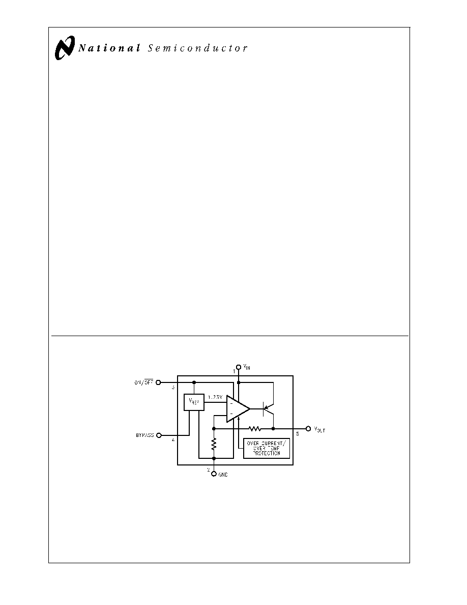
Block Diagram
VIP
TM
is a trademark of National Semiconductor Corporation.
DS100935-1
July 2000
LP2978
Micropower
SOT
,
5
0
m
A
Low-Noise
Ultra
Low-Dropout
Regulator
© 2000 National Semiconductor Corporation
DS100935
www.national.com
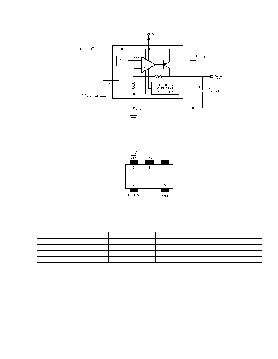
Basic Application Circuit
Connection Diagram
Ordering Information
TABLE 1. Package Marking and Ordering Information
Output Voltage (V)
Grade
Order Information
Package Marking
Supplied As:
3.8
A
LP2978AIM5X-3.8
LÿLA
3000 Units on Tape and Reel
3.8
A
LP2978AIM5-3.8
LÿLA
1000 Units on Tape and Reel
3.8
STD
LP2978IM5X-3.8
LÿLB
3000 Units on Tape and Reel
3.8
STD
LP2978IM5-3.8
LÿLB
1000 Units on Tape and Reel
DS100935-2
*ON/OFF input must be actively terminated. Tie to V
IN
if this function is not to be used.
**Minimum capacitance is shown to ensure stability (may be increased without limit). Ceramic capacitor required for output (see Application Hints).
***Reduces output noise (may be omitted if application is not noise critical). Use ceramic or film type with very low leakage current (see Application Hints).
DS100935-3
See NS Package Number MF05A
LP2978
www.national.com
2
Absolute Maximum Ratings
(Note 1)
If Military/Aerospace specified devices are required,
please contact the National Semiconductor Sales Office/
Distributors for availability and specifications.
Storage Temperature Range
-65∞C to +150∞C
Operating Junction Temperature Range
-40∞C to +125∞C
Lead Temp. (Soldering, 5 sec.)
260∞C
ESD Rating (Note 2)
2 kV
Power Dissipation (Note 3)
Internally Limited
Input Supply Voltage (Survival)
-0.3V to +16V
Input Supply Voltage (Operating)
2.5V to +16V
Shutdown Input Voltage (Survival)
-0.3V to +16V
Output Voltage (Survival, (Note 4))
-0.3V to +9V
I
OUT
(Survival)
Short Circuit
Protected
Input-Output Voltage (Survival,
-0.3V to +16V
(Note 5))
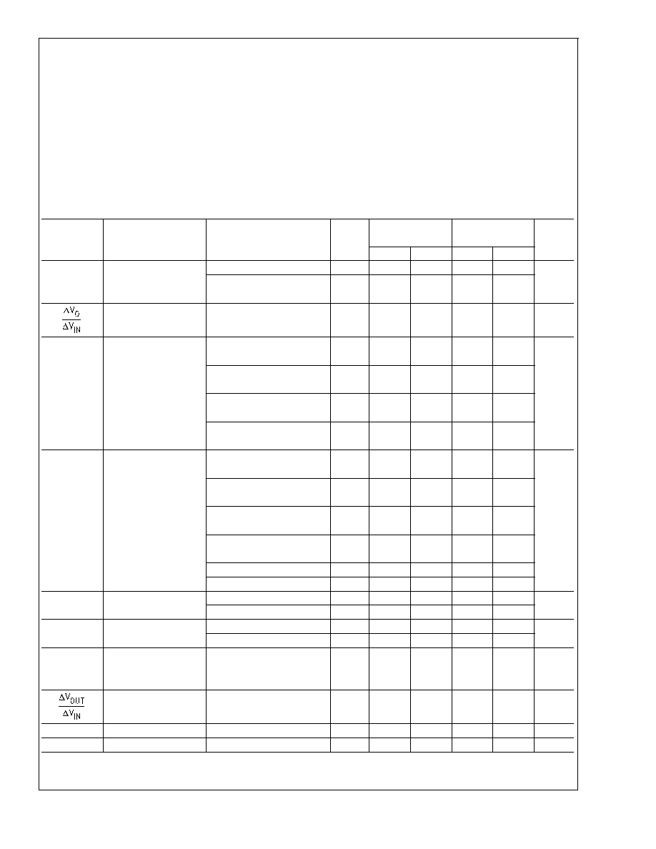
Electrical Characteristics
Limits in standard typeface are for T
J
= 25∞C. and limits in boldface type apply over the full operating temperature range. Un-
less otherwise specified: V
IN
= V
O
(NOM) + 1V, I
L
= 1 mA, C
IN
= 1 µF, C
OUT
= 4.7 µF, V
ON/OFF
= 2V.
Symbol
Parameter
Conditions
Typ
LP2978AI-X.X
LP2978I-X.X
Units
(Note 6)
(Note 6)
Min
Max
Min
Max
V
O
Output Voltage
Tolerance
I
L
= 1 mA
-1.0
1.0
-1.5
1.5
%V
NOM
1 mA
I
L
50 mA
-1.5
1.5
-2.5
2.5
-2.5
2.5
-3.5
3.5
Output Voltage
V
O
(NOM)+1V
V
IN
16V
0.007
0.014
0.014
%/V
Line Regulation
0.032
0.032
V
IN
≠V
O
Dropout Voltage
(Note 7)
I
L
= 0
1
3
3
mV
5
5
I
L
= 1 mA
7
10
10
15
15
I
L
= 10 mA
40
60
60
90
90
I
L
= 50 mA
120
150
150
225
225
I
GND
Ground Pin Current
I
L
= 0
65
95
95
µA
125
125
I
L
= 1 mA
75
110
110
170
170
I
L
= 10 mA
120
220
220
400
400
I
L
= 50 mA
350
600
600
1000
1000
V
ON/OFF
<
0.3V
0.01
0.8
0.8
V
ON/OFF
<
0.15V
0.05
2
2
V
ON/OFF
ON/OFF Input Voltage
(Note 8)
High = O/P ON
1.4
1.6
1.6
V
Low = O/P OFF
0.55
0.15
0.15
I
ON/OFF
ON/OFF Input Current
V
ON/OFF
= 0
0.01
-2
-2
µA
V
ON/OFF
= 5V
5
15
15
e
n
Output Noise
BW = 300 Hz to 50 kHz,
Voltage (RMS)
C
OUT
= 10 µF
30
µV
C
BYPASS
= 10 nF
Ripple Rejection
f = 1 kHz, C
BYPASS
= 10 nF
45
dB
C
OUT
= 10 µF
I
O
(SC)
Short Circuit Current
R
L
= 0 (Steady State)
400
mA
I
O
(PK)
Peak Output Current
V
OUT
V
o
(NOM) -5%
350
mA
Note 1: "Absolute Maximum Ratings" indicate limits beyond which damage to the component may occur. Electrical specifications do not apply when operating the
device outside of its rated operating conditions.
Note 2: The ESD rating of pins 3 and 4 is 1 kV.
LP2978
www.national.com
3
Electrical Characteristics
(Continued)
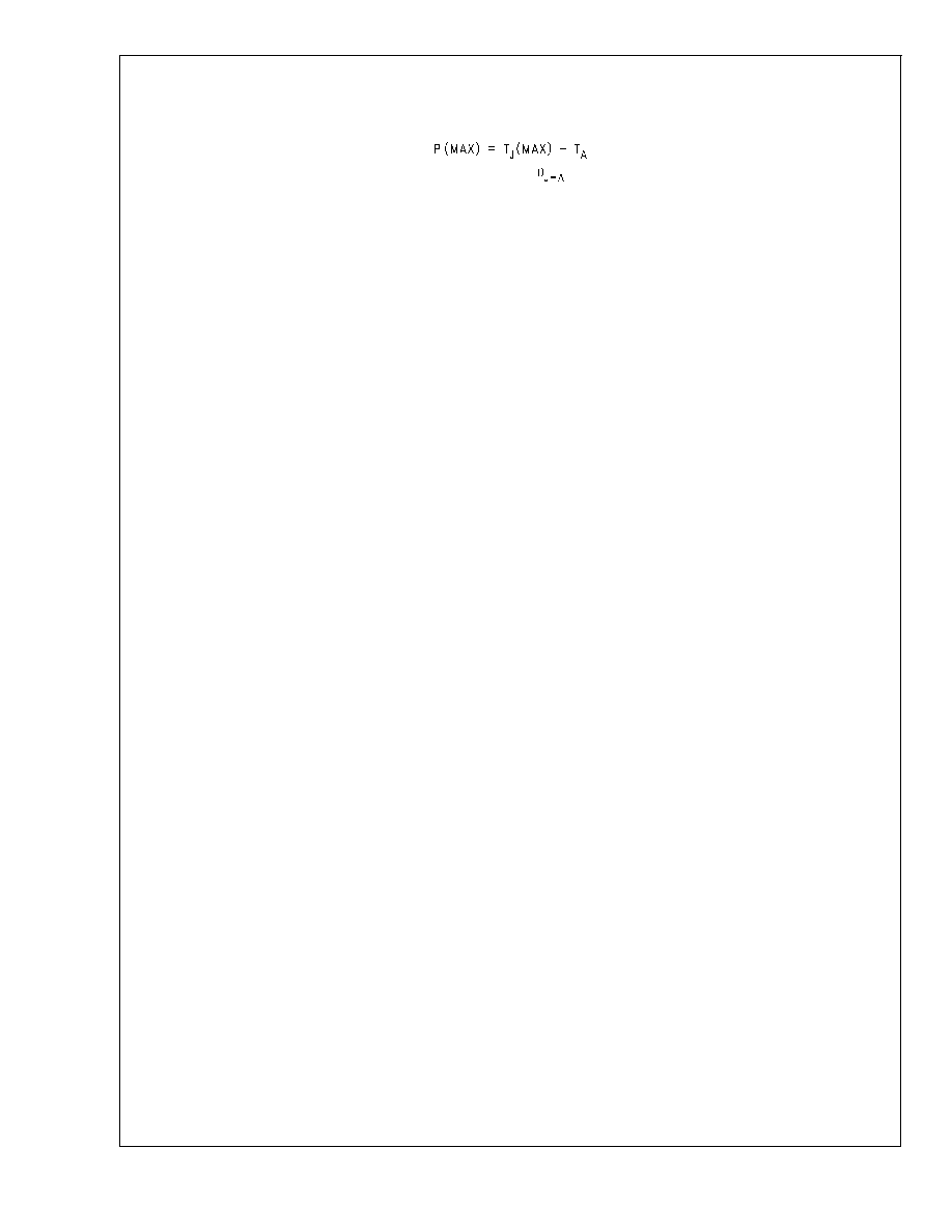
Note 3: The maximum allowable power dissipation is a function of the maximum junction temperature, T
J
(MAX), the junction-to-ambient thermal resistance,
J-A
, and
the ambient temperature, T
A
. The maximum allowable power dissipation at any ambient temperture is calculated using:
Where the value of
J-A
for the SOT-23 package is 220∞C/W in a typical PC board mounting. Exceeding the maximum allowable dissipation will cause excessive die
temperature, and the regulator will go into thermal shutdown.
Note 4: If used in a dual-supply system where the regulator load is returned to a negative supply, the LP2978 output must be diode-clamped to ground.
Note 5: The output PNP structure contains a diode between the V
IN
to V
OUT
terminals that is normally reverse-biased. Reversing the polarity from V
IN
to V
OUT
will
turn on this diode.
Note 6: Limits are 100% production tested at 25∞C. Limits over the operating temperature range are guaranteed through correlation using Statistical Quality Control
(SQC) methods. The limits are used to calculate National's Average Outgoing Quality Level (AOQL).
Note 7: Dropout voltage is defined as the input to output differential at which the output voltage drops 100 mV below the value measured with a 1V differential.
Note 8: The ON/OFF input must be properly driven to prevent possible misoperation. For details, refer to Application Hints.
LP2978
www.national.com
4
Application Hints
EXTERNAL CAPACITORS
Like any low-dropout regulator, the LP2978 requires external
capacitors for regulator stability. These capacitors must be
correctly selected for good performance.
Input Capacitor
An input capacitor whose capacitance is
1 µF is required
between the LP2978 input and ground (the amount of ca-
pacitance may be increased without limit).
This capacitor must be located a distance of not more than 1
cm from the input pin and returned to a clean analog ground.
Any good quality ceramic, tantalum, or film capacitor may be
used at the input.
Important: Tantalum capacitors can suffer catastrophic fail-
ure
due
to
surge
current
when
connected
to
a
low-impedance source of power (like a battery or very large
capacitor). If a Tantalum capacitor is used at the input, it
must be guaranteed by the manufacturer to have a surge
current rating sufficient for the application.
There are no requirements for ESR on the input capacitor,
but tolerance and temperature coefficient must be consid-
ered when selecting the capacitor to ensure the capacitance
will be
1 µF over the entire operating temperature range.
Output Capacitor:
The LP2978 is designed specifically to work with ceramic
output capacitors, utilizing circuitry which allows the regula-
tor to be stable across the entire range of output current with
an output capacitor whose ESR is as low as 5 m
. It may
also be possible to use Tantalum or film capacitors at the
output, but these are not as attractive for reasons of size and
cost (see next section Capacitor Characteristics).
The output capacitor must meet the requirement for mini-
mum amount of capacitance and also have an ESR (equiva-
lent series resistance) value which is within the stable range.
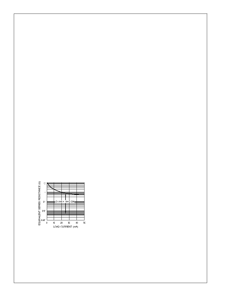
Curves are provided which show the stable ESR range as a
function of load current (see ESR graph below).
Important: The output capacitor must maintain its ESR
within the stable region over the full operating temperature
range of the application to assure stability.
The LP2978 requires a minimum of 2.2 µF on the output
(output capacitor size can be increased without limit).
It is important to remember that capacitor tolerance and
variation with temperature must be taken into consideration
when selecting an output capacitor so that the minimum re-
quired amount of output capacitance is provided over the full
operating temperature range. It should be noted that ceramic
capacitors can exhibit large changes in capacitance with
temperature (see next section,
Capacitor Characteristics).
The output capacitor must be located not more than 1 cm
from the output pin and returned to a clean analog ground.
Noise Bypass Capacitor:
Connecting a 10 nF capacitor to the Bypass pin significantly
reduces noise on the regulator output. It should be noted that
the capacitor is connected directly to a high-impedance cir-
cuit in the bandgap reference.
Because this circuit has only a few microamperes flowing in
it, any significant loading on this node will cause a change in
the regulated output voltage. For this reason, DC leakage
current through the noise bypass capacitor must never ex-
ceed 100 nA, and should be kept as low as possible for best
output voltage accuracy.
The types of capacitors best suited for the noise bypass ca-
pacitor are ceramic and film. High-quality ceramic capacitors
with either NPO or COG dielectric typically have very low
leakage. 10 nF polypropolene and polycarbonate film ca-
pacitors are available in small surface-mount packages and
typically have extremely low leakage current.
CAPACITOR CHARACTERISTICS
The LP2978 was designed to work with ceramic capacitors
on the output to take advantage of the benefits they offer: for
capacitance values in the 2.2 µF to 4.7 µF range, ceramics
are the least expensive and also have the lowest ESR val-
ues (which makes them best for eliminating high-frequency
noise). The ESR of a typical 2.2 µF ceramic capacitor is in
the range of 10 m
to 20 m
, which easily meets the ESR
limits required for stability by the LP2978.
One disadvantage of ceramic capacitors is that their capaci-
tance can vary with temperature. Most large value ceramic
capacitors (
2.2 µF) are manufactured with the Z5U or Y5V
temperature characteristic, which results in the capacitance
dropping by more than 50% as the temperature goes from
25∞C to 85∞C.
This could cause problems if a 2.2 µF capacitor were used
on the output since it will drop down to approximately 1 µF at
high ambient temperatures (which could cause the LP2978
to oscillate). If Z5U or Y5V capacitors are used on the output,
a minimum capacitance value of 4.7 µF must be observed.
A better choice for temperature coefficient in ceramic capaci-
tors is X7R, which holds the capacitance within
±
15%. Un-
fortunately, the larger values of capacitance are not offered
by all manufacturers in the X7R dielectric.
Tantalum:
Tantalum capacitors are less desirable than ceramics for use
as output capacitors because they are more expensive when
comparing equivalent capacitance and voltage ratings in the
1 µF to 4.7 µF range.
Another important consideration is that Tantalum capacitors
have higher ESR values than equivalent size ceramics. This
means that while it may be possible to find a Tantalum ca-
pacitor with an ESR value within the stable range, it would
have to be larger in capacitance (which means bigger and
more costly) than a ceramic capacitor with the same ESR
value.
DS100935-7
LP2978
www.national.com
5